

Another Giant Leap: The Rubin CPX Specialized Accelerator & Rack
New Prefill Specialized GPU, Rack Architecture, BOM, Disaggregated PD, Higher Perf per TCO, Lower TCO, GDDR7 & HBM Market Trends
Nvidia announced the Rubin CPX, a solution that is specifically designed to be optimized for the prefill phase, with the single-die Rubin CPX heavily emphasizing compute FLOPS over memory bandwidth. This is a game changer for inference, and its significance is surpassed only by the March 2024 announcement of the GB200 NVL72 Oberon rack-scale form factor. Only with hardware specialized to the very different phases of inference, prefill and decode, can disaggregated serving achieve its full potential.
As a result, the rack system design gap between Nvidia and its competitors has become canyon-sized. AMD and custom silicon competitors may have made a small step forward in emulating Nvidia’s 72-GPU rack scale design, but Nvidia has just made another Giant Leap, again leaving competitors very distant objects in the rear-view mirror.
AMD and ASIC providers have already been investing heavily to catch up in terms of their own rack-scale solutions. AMD in particular has been working tirelessly to improve their software stack to try to close the gap with Nvidia, but now everyone will needs to redouble their investments yet again as they will have to develop their own prefill chips, delaying further the timeframe with which they can close this gap. With this announcement, all of Nvidia’s competitors will be sent back to the drawing board to reconfigure their entire roadmaps again in a repeat of how Oberon changed roadmaps across the industry.
The Rubin CPX
Because the prefill stage during inference tends to heavily utilize compute (FLOPS) and only lightly use memory bandwidth, running prefill on a chip with lots of expensive HBM featuring very high memory bandwidth is a waste. The answer is a chip that is skinny on memory bandwidth and relatively fat on compute. Enter the Rubin CPX GPU.
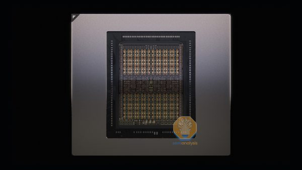
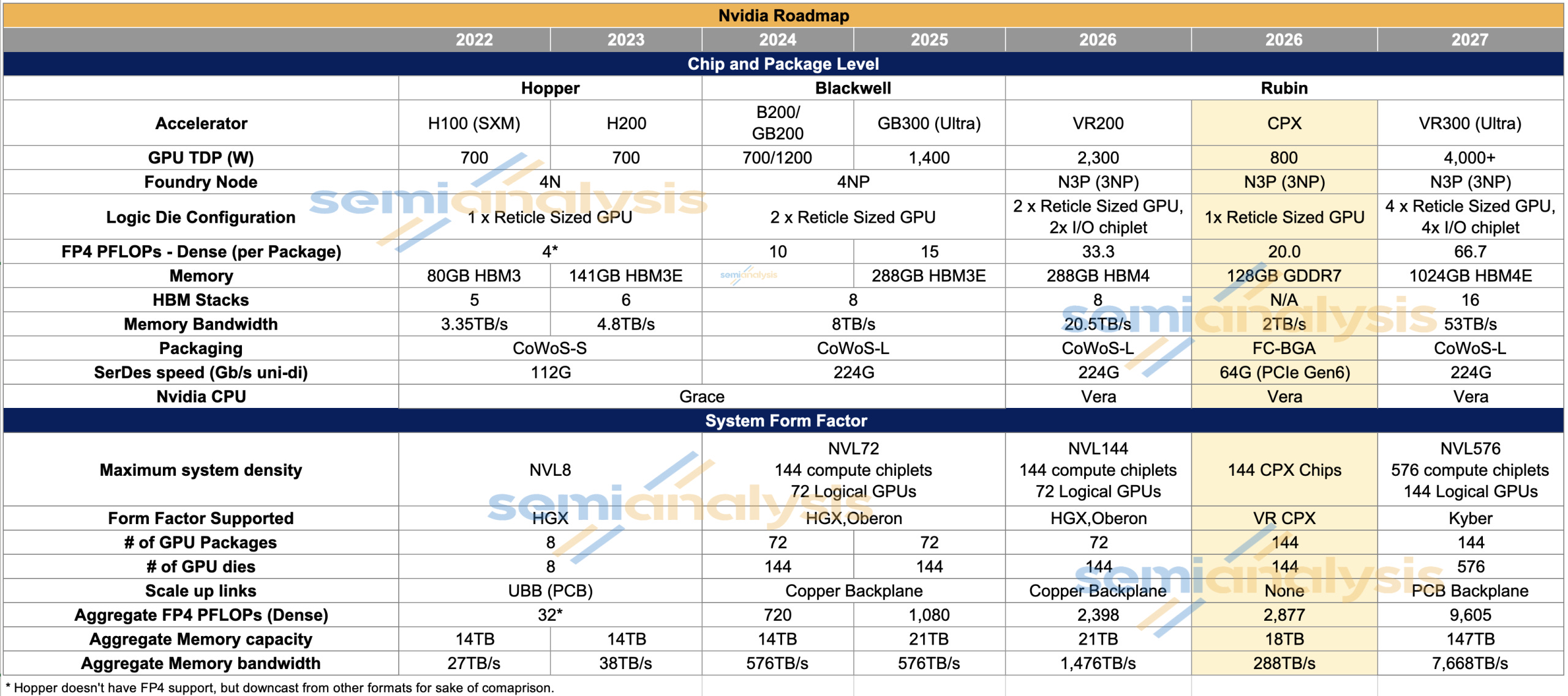
The Rubin CPX features 20 PFLOPS of FP4 dense compute but only 2TB/s of memory bandwidth. It also features 128GB of GDDR7 memory, a lower quantity of less expensive memory when compared to the VR200. By comparison, the dual-die R200 chip offers 33.3 PFLOPS of FP4 dense and 288GB of HBM offering 20.5 TB/s of memory bandwidth.
The introduction of the Rubin CPX expands the VR200 family of rack scale servers into three flavors:
VR200 NVL144: 72 GPUs packages across 18 compute trays, with 4 R200 GPU packages in each compute tray.
VR200 NVL144 CPX: 72 Logical GPUs packages in addition to 144 Rubin CPX GPU packages across 18 compute trays, with 4 R200 GPU packages and 8 Rubin CPX GPU packages in each compute tray.
Vera Rubin CPX Dual Rack: Two discrete racks – one VR200 NVL144 rack plus one VR CPX rack with 144 Rubin CPX GPUs across 18 compute trays, with 8 Rubin CPX GPUs in each compute tray.

In this report, we will first explain the story so far and the impetus for the development of the Rubin CPX because of the different role memory plays during prefill and decode phases of inference. We will then dive deep into the architecture of the Rubin CPX chip and the rack-scale solutions where it is deployed. We will then shift focus from the past and present to what the future holds with respect to disaggregated inference serving and how today’s announcement impacts future roadmaps and competitiveness for other merchant accelerator providers and custom silicon projects. In the final part of this article, we will briefly present a comprehensive list of key bill of materials (BoM) items for both racks and a power budget analysis by major component groups.
Memory: The Story So Far
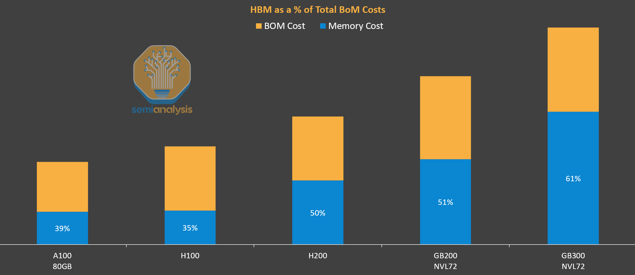
The memory wall has been the most important constraint for AI. Larger memory capacities have been necessary to load larger models into accelerators, while memory bandwidth has been the main gating factor for inference and training token throughput. This is why high bandwidth memory (HBM) capacity and bandwidth per GPU have increased rapidly – from 80GB and 3.4TB/s for the H100 to 288GB and 8.0TB/s for the GB300, more than tripling memory capacity and increasing bandwidth by ~2.5x in less than three years.
Consequently, HBM has consistently increased as a % of accelerator BOM from Hopper to Blackwell, with HBM now being the largest single component of the package BOM for the GB300. HBM is extremely valuable for both training and inference, but when we break down inference to its constituent parts of prefill and decode steps, HBM only has high value for the decode step. During prefill, which is compute intensive, the generation of KVCache is much less bandwidth intensive due to the parallel nature of prefill, therefore the HBM is underutilized during this step.
HBM carries such an expensive premium relative to other forms of DRAM because of its additional bandwidth, and when this B/W is underutilized, this HBM is “wasted”. The escalating proportion of BOM taken up by HBM presents yet another “wall” and is the impetus behind the development of the Rubin CPX GPU.
Now that we have briefly explored the role memory has played thus far, let’s pivot to today’s announcement and explore in detail the architecture of the Rubin CPX and the rack scale servers where it is deployed.
Bandwidth and Compute Difference
Each Rubin CPX chip will be a monolithic SoC on a conventional flip chip BGA package. Instead of HBM, Rubin CPX will have 128GB of GDDR7 DRAM. Switching from using HBM to cheaper GDDR7 memory reduces the cost per GB by more than 50%.
Memory speeds will likely be at 32Gbps with a 512-bit bus. This results in 2TB/s of memory bandwidth per Rubin CPX compared to 20.5TB/s of memory bandwidth per R200. Notably, with this keynote, Nvidia also confirms a significant bandwidth upgrade for regular Rubin. R200’s HBM4 speeds have been significantly increased to 10Gbps to achieve 20.5TB/s of memory bandwidth per R200 as we discussed in the Accelerator and HBM model previously. This compares to the R200 being first unveiled as "only" having 13TB/s of memory bandwidth specifications at a 6.4Gbps speed bin. We discussed and quantify the impacts to HBM suppliers in the model as well. The 144 CPX chips that each deliver 2.0 TB/s of memory bandwidth and the 72 R200 chips that deliver 20.5TB/s will combine to deliver total system memory bandwidth of 1.7PB/s.
For compute, each CPX offers 30 PFLOPs of sparse FP4 computing throughput (20 PFLOP dense) compared to the R200 at 50 PFLOPs sparse FP4 (33.3 PFLOPs dense). Dense PFLOPs for the Rubin CPX follow the same 3:2 sparse to dense ratio as the R200 because it inherits a similar tensor core architecture as Rubin R200. The CPX offers very strong FP4 compute throughput for a single compute die relative to the two dies for R200. The gains are likely from reducing higher precision compute units to have more FP4 ALUs. This was what was implemented with the B300 to get higher FP4 throughput than the B200 while staying on the same 4NP node.
However, as always, peak theoretical FLOPs are extremely hard to attain in practice. Like Nvidia’s other GPUs that are power-limited, it will be very difficult for Rubin CPX to sustain anywhere close to peak FLOPs given what we estimate to be rated power of only around 800W: we do not see it feasible to break past 1W/mm2 of power density, especially as the board comes is integrated in a sandwiched form factor (more on this below).
What is also different is the network. There is no NVLink SerDes for scale-up, instead Rubin CPX relies on PCIe Gen 6 to talk to other GPUs through the CX-9 NICs on the scale-out network. This reduced network capability is more than feasible through implementing pipeline parallelism which we discuss below.
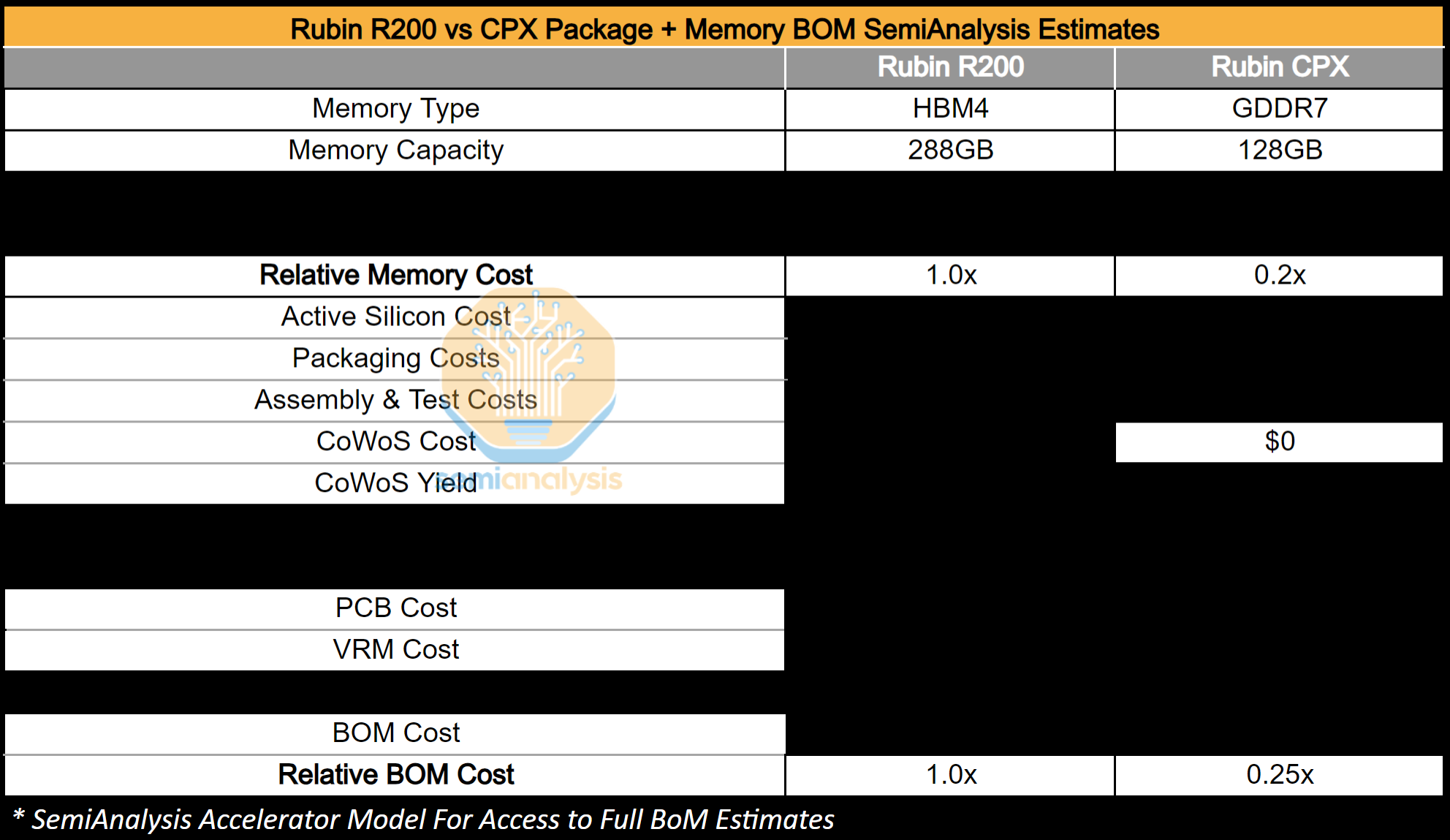
Because of the lower total silicon content and less expensive memory, the production cost of Rubin CPX is drastically lower than that of the R200. Lowering total memory capacity and using lower cost GDDR7 means that memory cost is 5x lower. The chip architecture is also far simpler since avoiding HBM and only have a single reticle-sized die without any I/O chiplets means CoWoS packaging is not required. For perspective, the design of Rubin CPX is similar to a next-generation RTX 5090 or RTX PRO 6000 Blackwell, as both use a large monolithic die with a 512-bit wide GDDR7 memory interface. As these chips are based on the consumer Blackwell GPU die, those chips only have 20% of the FLOPS as their HBM-enabled big brother, the B200. With Rubin CPX, this ratio jumps to 60% as it will be a separate tapeout that looks closer to the R200 compute die. As an exercise in achieving maximum FLOPS per unit cost - Rubin CPX is unmatched.
Later in the article, we will break down the BOM advantage of Rubin CPX and estimate how much can be saved by moving prefill off R200 and onto Rubin CPX.
Nvidia Oberon Rack Architecture Upgrade: VR NVL144 CPX, VR NVL144, VR CPX
Let’s move outside of the Rubin CPX chip and into the two new Vera Rubin racks that will host the CPX.
In March of last year, at GTC 2024, Nvidia presented the first generation of its Oberon Architecture: the GB200 NVL72. Fast forward a year and a half later, the second generation of Oberon, the GB300 NVL72, is about to ship in mass production volume. There are very few design changes and upgrades between the two generations. The third generation of Oberon architecture, Vera Rubin (VR), was the focus of Ian’s talk today at the AI Infra Summit. Available in 2026, less than three years after the debut of the Oberon rack-scale form factor, VR will see significant design changes and upgrades from GB200/GB300.
Vera Rubin Oberon pushes power density of the Oberon architecture to its limits, requiring a significant upgrade in power delivery content and design changes in cooling solutions. The cableless design is chosen with consideration to overcome the difficulties with routing flyover cables in the GB200/GB300 assembly & the reliability challenges that the intra-tray cables caused. The cables connecting the OSFP cages to the ConnectX NIC have been removed. Cables connecting from PCIe to the frontend Bluefield DPU & to local NVMe storage have also been removed amongst other side band cables.
The key changes and upgrades found in Vera Rubin are focused on a revamp of the following three Vera Rubin (VR) Compute Tray SKUs:
VR NVL144 (Rubin Only)
VR CPX (Rubin CPX Only)
VR NVL144 CPX (Rubin + Rubin CPX in same tray)
These three compute tray flavors are the building blocks for the three rack solutions discussed:
VR NVL144
VR NVL144 CPX
VR NVL144 + VR CPX (Dual Rack)
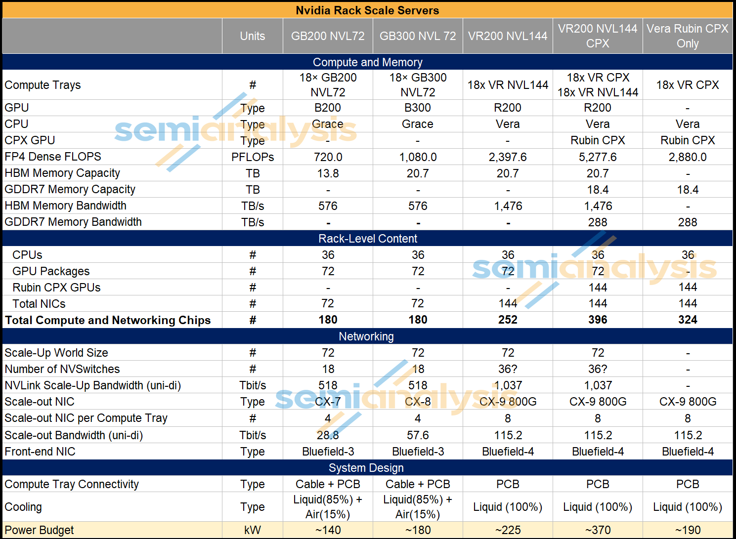
The first rack presented was the VR NVL144 CPX. This is similar to the VR NVL144, except that for the VR NVL144 CPX, in each of the 18 Compute Trays, in addition to 4 R200 GPUs and 2 Vera CPUs, we now also have 8 Rubin CPX GPUs in each compute tray as well.
The VR NVL144 CPX rack will also be liquid cooled – but will have a much higher power budget at ~370kW vs the ~190kW for the VR NVL144.
The other deployment option is the Vera Rubin CPX Dual Rack. As the name suggests, this solution allows customers that will have deployed VR NVL144 racks to subsequently add VR CPX racks to their datacenter later, enabling specialized hardware for disaggregated PD inferencing. VR CPX is not connected via NVLink, hence the VR CPX rack does not contain NVSwitch Trays. The VR CPX rack is connected to the cluster through scale-out InfiniBand or Ethernet networking and can be added on subsequently to a cluster in a convenient physical location – it need not be physically adjacent to a VR NVL144.
The dual rack solution offers a lot more flexibility compared to VR NVL144 CPX as the customers can design the prefill to decode ratio to their likings. Also, not everyone’s datacenter infra will be ready for the ~370kW VR NVL144 CPX. In addition there is a smaller blast radius of failures compared to the single rack variant.
In the table below, we can see how much compute and networking content is crammed into one compute tray – a total of 22 Nvidia chips (14 of them being XPUs) in each compute tray, or 396 chips per VR NVL144 CPX rack. To cram all this content above into a single compute tray, Nvidia has moved to a cableless and modular design and is also redesigning the cooling loops within the compute tray.

The NVL144 CPX will maintain a similar compute board set up as GB200/GB300 for the back half of the compute tray chassis. The notable difference is the adoption of socketable SOCAMM DRAM modules instead of soldered LPDDR5X for the memory that runs off the CPU. Most of the difference between VR NVL144 CPX and GB200/GB300 is in the front half of the chassis below the Host Processor Motherboard (‘HPM’) compute board, also known as the “Bianca” board for Blackwell generation.
At the front, the VR NVL144 CPX design is modular made up of 7 daughter card modules.
Four daughter card modules are placed on both sides of the chasis. Each side has two daughter cards stacked on top of each other. These four daughter cards each contain two 800G CX-9 NICs, one 1.6T OSFP cage, one E1.S SSD NVMe Module, and two Rubin CPXs.
One daughter card in the middle of the chassis (lower center of the diagram below) houses the Bluefield-4 Module, which contains one grace CPU and one CX-9 NIC.
One daughter card stacked on top of this Bluefield-4 module houses the power delivery board (PDB). The PDB is responsible for stepping down power from 48-54V to 12-13.5V as it enters the chassis from the busbar connector at the back.
The last daughter card is much smaller and is placed just to the right of the Bluefield-4 module. It is much slimmer and houses the utility management module containing items such as the BMC, HMC, DC-SCM, and management I/O.


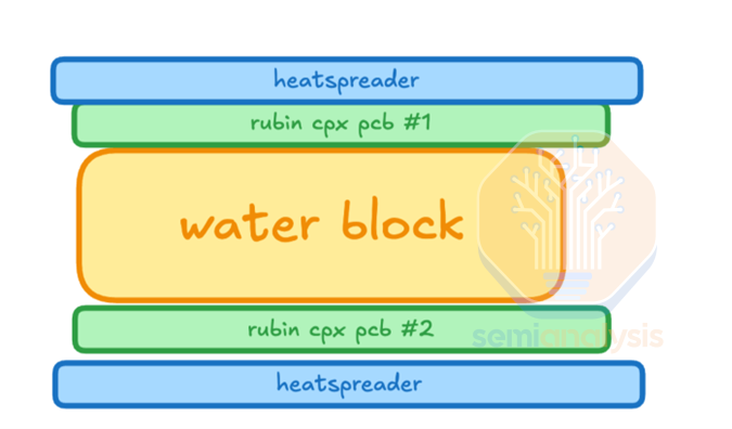
We estimate the TDP of the Rubin CPX chip to be around 800W, though that rises to 880W in total when factoring in the whole module which contains the GDDR7 memory. To cool down the 7,040W of Rubin CPX modules at the front of the compute tray, the front of chassis cooling must be upgraded from air cooling to liquid cooling.
To accomplish this, NVIDIA has brought back a design from its 2009 GTX 295. The Rubin CPX and CX9 daughter cards are arranged in a sandwiched design with a shared liquid-cooled cold plate in between.


On the outer sides of the PCBs, heat pipes and heat spreaders transfer heat from the back of each clamshell GDDR7 memory modules to the main cold plate. Halving the compute tray area needed to house these GPUs by making full use of the 1U tray height and using both sides of the cold plate allows for maximum density.
Another key design change of VR NVL144 CPX is the adoption of cableless design. As we discussed in our PCB Supercycle Core Research note as well as our recent Core Research note on Amphenol’s AI Content, there are two reasons for this design. First, flyover cables present multiple different points of failure as they can easily be damaged during assembly. Second, the high-density design of VR NVL144 CPX leaves no space for cables to be routed.
So how are the signals routed without cables? The answer is simple: signals from the HPM (Bianca) board travel off the board via the Paladin board to board connector from Amphenol. This is discussed in more detail in our recent article on Amphenol’s AI Content. The signal is then routed through a PCB midplane sitting in the middle of the chassis. On the other side of the PCB midplane, the daughter cards connect to the PCB midplane via another set of Paladin B2B connectors.


To accommodate this cableless design, the CX-9 NICs on the upper part of the HPM (Bianca) board are moved from the back half to the front half of the chassis as illustrated in the diagram below. For the GB200/GB300, the PCIe signal distance between the GPU/CPU and the CX-7/8 is shorter than the Ethernet/Infiniband signal distance between the CX-7/8 and the OSFP cages.
Previously – having to transmit a 200G Ethernet/InfiniBand signal from the NIC in the back half of the compute tray to the OSFP cage in the front of the compute tray necessitated the use of flyover cables as the signal loss over PCB at 200Gbit/s (uni-directional) per lane is too high.
But now that the NIC is closer to the OSFP cage, the lower speed per lane PCIe Gen6 signals (64Gbit/s per lane uni-directional) travel the longer distance, and this connectivity can now be routed over PCB. Although it is still challenging to drive PCIe Gen6 signals over PCB, proper signal integrity can still be achieved by upgrading PCB materials.


For better serviceability, the daughter cards are also designed as a module. Each daughter card module can slide in and out of the daughter card module bay. Within the compute tray, there are internal rail kits designed for this purpose.
Below we show how the signals are routed within different Vera Rubin compute tray SKUs as well as the compute tray topology of the VR Rubin SKUs. One highlight from these diagrams is that CX-9 plays a critical role in enabling Rubin CPX and scale out connections, as it is an integrated PCIe switch too.


The Giant Leap: Disaggregated Serving
Today’s announcement of Rubin CPX is a game changer for inference, and its significance is surpassed only by the first announcement of the GB200 NVL72 Oberon rack-scale form factor. Only with hardware specialized to the very different phases of inference, prefill and decode, can disaggregated serving truly be attained.
In this section we will explain the evolution from traditional serving to disaggregated serving with uniform hardware and end with an analysis on disaggregated serving with specialized hardware. We will demonstrate how much waste is incurred by disaggregated serving with uniform hardware. Once specialized inference hardware becomes ubiquitous, using uniform hardware will feel like buying a jackhammer to squash a bug.
As we mentioned earlier in the article, the release of the Rubin CPX will send Nvidia’s competitors back to the drawing board to reshape their roadmaps. To not release a prefill specialized chip of their own will mean saddling their own customers with inefficient systems that will guarantee those customers will lose in the tokenomics marketplace.
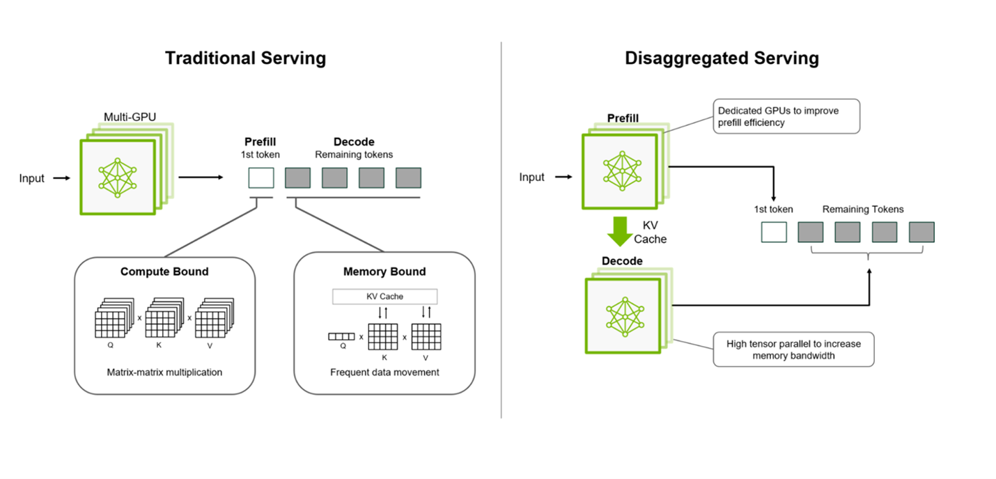
Serving an LLM request involves two phases: the prefill phase and decode phase. In the prefill phase, the LLM generates the first token from the user prompt. This phase affects the time-to-first token (TTFT), and it is usually compute-bounded, under-utilizing the memory bandwidth. On the other hand, the decode phase generates a new token while loading the previous tokens from the KV cache. This phase affects time-per-output-token (TPOT), and it is always memory-bounded, under-utilizing the compute.
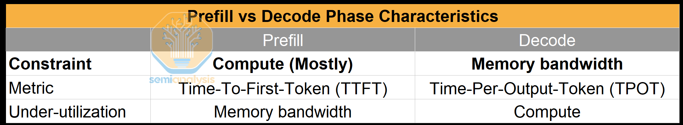
In the chart below, we see an illustrative example highlighting the tradeoff between memory bandwidth and FLOPS utilization when conducting prefill and decode on the same system. The FLOPS required to prefill a single token scales linearly with respect to input sequence length. FLOPS requirements for decode also scales with respect to users on the system (i.e. batch size) and sequence lengths.
A short input sequence length may not fully saturate the FLOPS available on an inference system, in which case the system’s output will be limited by the speed at which parameters can be loaded into chip memory – which is a function of memory bandwidth. As input sequence length increases, however, eventually the workload will grow to use all available FLOPS on the inference system, and the workload will be constrained by the total system FLOPS. In the right half of the chart below, we illustrate that when sequence length exceeds 32k, the FLOPS utilization reaches 100% while the memory bandwidth utilization drops.
Thus we can see that when a node is conducting a very prefill heavy workload – with long sequence lengths or large batch sizes, the memory bandwidth goes unutilized. As mentioned in the previous section, with the % of Chip BOM dedicated to memory increasing continually over the past few years, this ends up being a very expensive underutilization of resources!
Inefficiency also comes from the fact that the workload characteristics of the prefill and the decode phases are so inherently different that prefill and decode requests always interfere with each other’s performance when they are processed concurrently. There are many optimizations to try to balance both – for example adding prefill calculations to decide to ensure a somewhat uniform request length to improve utilization, but they always result in tradeoffs. Another approach is to separate the prefill and decode phases completely, but if you prioritize the decode phase, then your prefill will need to wait – resulting in a long time to first token. Conversely, if you prioritize prefill, your decode phase will be forced to wait and your inter-token latency will be slow as memory bandwidth then goes underutilized.
An Initial Step: Disaggregated Prefill and Decode with the Same Hardware
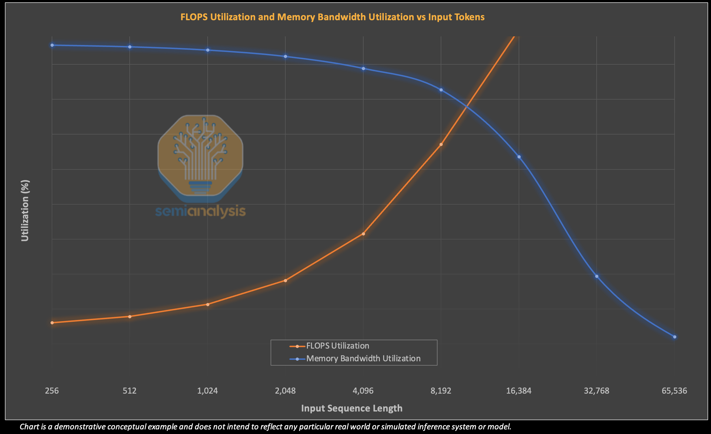
The first order solution is to implement disaggregated serving to first tackle the interference by routing prefill and decode requests to separate compute units, making it simpler to reason about performance. This has the benefit of being able to better manage service level agreements (SLAs) that tend to focus on a certain level of token/s/user. There are a few catches however. This complete disaggregation only seems to provide excellent results under certain input/output sequence length ratios and for long decode lengths, with other scenarios seeing underwhelming benefits. In addition, this disaggregation still leaves the “wrong sizing” problem whereby a pure prefill operation will almost always heavily underutilize memory bandwidth.
In the illustrative example below, we show how an R200 would hardly use much of its memory bandwidth when being used solely for prefill. As we increase sequence length and more efficiently use FLOPS available, the memory bandwidth utilization becomes increasingly minimal – effectively wasting very expensive HBM memory.
The Next Step: Disaggregated Prefill and Decode on Specialized Hardware – Enter the Rubin CPX
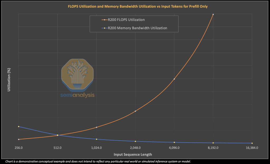
Since prefill is inherently going to underutilize memory bandwidth resources one approach to reduce wastage is to reduce the quantity and cost of the memory. This is exactly the approach the Rubin CPX has taken by using lower quantities of less expensive GDDR7 memory.
In the illustrative example below, we show how an R200 hardly use much of its memory bandwidth when being used solely for prefill. In contrast, the Rubin CPX actually utilizes a higher percent of its memory bandwidth at fairly short input lengths before dropping even further for input lengths that we would consider typical.
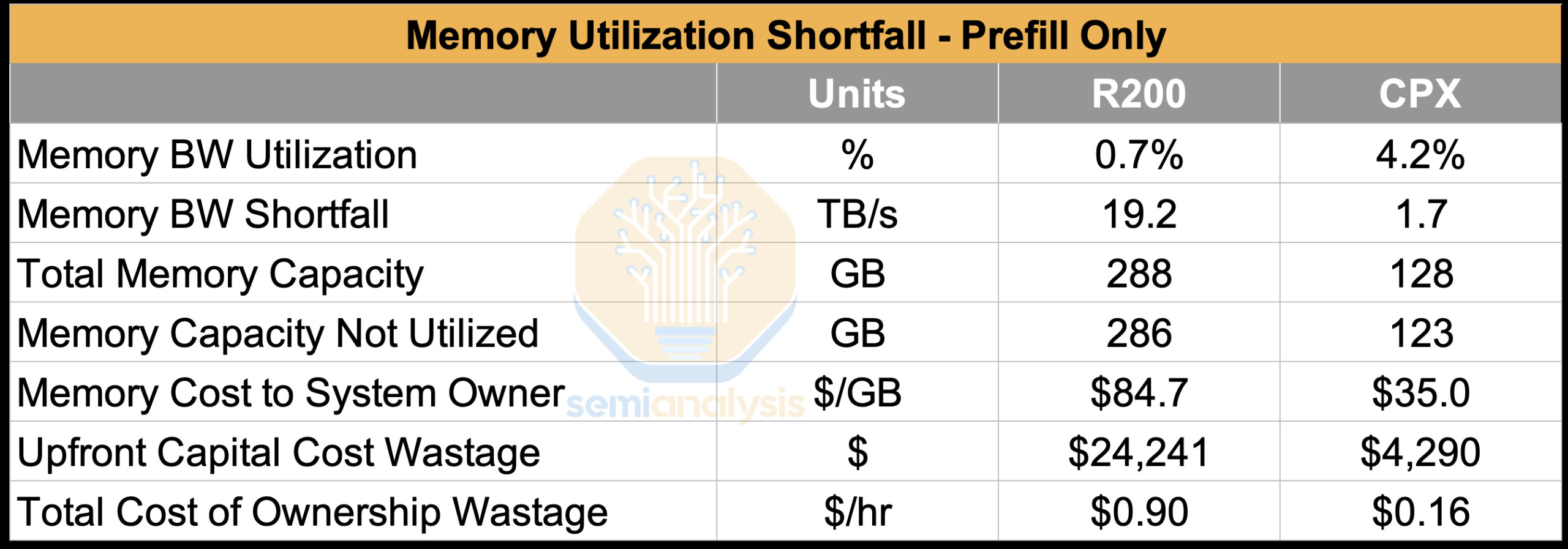
Indeed, we stress this is not about efficiency for efficiency’s sake –and there is a huge impact to the bottom line! In the table below, we use provide an example to compare the memory bandwidth utilization for the R200 GPU and the Rubin CPX GPU. In this scenario, both suffer from very low memory bandwidth utilization, but the difference is that the Rubin CPX GPU is at least leaving lower quantities of far less expensive memory on the table. For the R200 – we see that the exact same prefill workload as is run on the CPX results in a $0.90/hr total cost of ownership wastage!
Rubin CPX brings more memory capacity but the bits are “lower quality” as they are GDDR7, which is less than half the cost of HBM on a per GB basis. From a memory vendor perspective, GDDR7 is less margin because it is a less technically demanding product with more competition (i.e. Samsung can supply it).
What this means is that the use of CPX systems lowers HBM’s share of total system content. For every dollar spent on the VR200 NVL144 CPX or a VR CPX rack, a lower share of that dollar is spent on HBM when compared to the same dollar spend on a standalone VR200 NVL144 rack. All else being equal, assuming a fixed dollar spent on AI systems, HBM demand per dollar spent will decline.
Why Not Just Reduce Memory Further?
Many readers are doubtless salivating at the idea of spending less on HBM and are thinking: Why not curtail the amount of memory in a system even further? If a typical prefill sequence length means a memory utilization of low double digits or even single digits - why not reduce memory capacity to 1/10th the size? Does this mean doom for HBM demand and memory demand in general?
However, things are not so simple in technology. What Rubin CPX does is reduce the cost of pre-fill and tokens. Lower cost of tokens increases demand, which means more demand for decode increases as well. Like many other technological innovations that drive down cost, increases in demand usually more than offsets a drop in cost, netting out to a higher total dollar market size.
There are additional supply chain implications of this GDDR7 demand. The RTX Pro 6000 also uses GDDR7 but at a lower 28Gbps speed. Nvidia has put in huge supply chain orders for the RTX Pro SKU, with the original plan being to sell chips to China as a replacement for the H20 before export licenses for the H20 were reissued. These orders were primarily placed with Samsung, who had the capacity to meet these sudden rush orders. SK Hynix and Micron were not able to meet this demand as their wafer capacity was tied up to serve their HBM orders among other things. As Samsung can deliver competitive GDDR7, Samsung could similarly benefit from the Rubin CPX.
More on Prefill Pipeline Parallelism: One Interesting Upside of Disaggregated Prefill with the Rubin CPX
In the prior section we outlined how the Rubin CPX reduces memory wastage, but Rubin CPX foregoes the use of very fast scale-up network capabilities solutions such as NVLink is another key saving. Rubin CPX’s off-chip I/O is limited to 16 lanes of PCIe Gen6 which is approximately 1Tbit/s of unidirectional bandwidth vs 14.4Tbit/s of NVLink for R200. This is enough I/O for performing prefill even for modern MoE frontier LLMs.
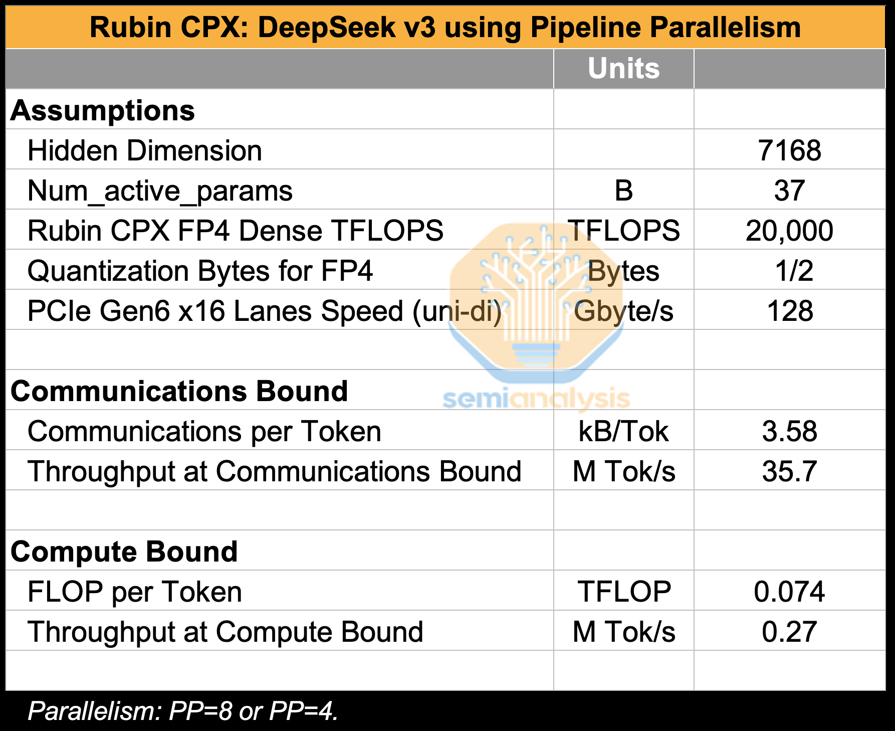
For instance, DeepSeek V3 when running on the NVFP4 number format will require 335GB of memory capacity to load all the model weights – this exceeds the 128GB of memory capacity of a single CPX chip. This can be overcome by using pipeline parallelism (‘PP’), where multiple layers of a model are split across different GPUs. In PP, each GPU processes tokens sequentially and will pass activations down the pipeline.
The disadvantage of PP is that the tokens are passed sequentially across many GPUs, incurring latency from inter-stage communications. The important implication is that PP will tend to deliver higher token throughput per GPU than Expert Parallelism (EP), but the tradeoff is that PP suffers from a higher time to first token (TTFT) than EP. PP has higher tok/s/gpu throughput because EP has high communications overhead as it involves all-to-all collective operations vs a simple send and receive operation in the case of PP.
So, for pipeline parallel inference, the simpler communications requirements mean that prefill will almost never saturate communications links – meaning there is no need to provision expensive fast scale-up networking. Like with HBM, this is another area where one can find savings by peeling away yet another layer of equipment that goes unused during prefill-only operations – sparing the system owner wasted TCO dollars.
In the table below, we show that prefill for DeepSeek using a parallelism scheme of PP8 or PP4 results in a message size per token of 7kB. If we were to fully saturate the PCIe Gen6 x16 lanes of I/O with messages, this means we could at most transmit (and therefore process) 18.3M tokens per second. This is the communications bound.
Turning to the compute bound scenario, we see that prefill FLOP per token is 0.074 TFLOP. So, if we divide the Rubin CPX’s dense FP4 throughput of 19,800 PFLOPS by 0.074 TFLOP, we arrive a maximum token throughput of 267.6k tokens/second.
This is far below the communications bound and vastly under saturates even a fairly vanilla PCIe Gen6 I/O let alone NVLink which delivers over 14x the bandwidth of 16 lanes of PCIe Gen6.
We estimate that the total NVLink Scale-up cost to the end system owner (inclusive of NVSwitches and Backplane) stands at around ~$8k per GPU – which is just over 10% of the all-in cluster cost per GPU. This is the other dimension along which Rubin CPX delivers considerable savings to the end user.
However, attempting to use Expert Parallelism with lower speed networking connectivity will lead to latency issues and bottlenecks. Communications need scale with respect to the product of top_k times number of layers. DeepSeek V3 has a top_k of 8 and has 61 layers, so a back of the envelope calculation would indicate that using EP over PP would increase communications requirements by ~488x.
One More Thing on Scaling and Huang’s Law
Today’s discussion focused on metrics for inference using the NVFP4 number format. Indeed, inference providers have been continually unlocking more throughput by pulling the level of adopting lower and lower precision number formats. However – once we are at FP4 – we will start to run out of juice to squeeze.
Sparsity has been presented as another lever to pull to keep unlocking more throughput, a key reason why most marketing specifications and decks communicate in terms of Sparse TFLOPS, however sparsity has yet to actually deliver the promised benefits – falling well short of the 2x pickup it promises.
Today’s announcement also unveiled sparsity for Rubin. This sparsity scheme is unlike the 2:4 structured sparsity used in Hopper and Ampere, and it isn’t like Blackwell’s 4:8 pairwise structured sparsity either. We hope Rubin Sparsity is able to yield meaningful throughput benefits and keep Huang’s law on track!
Downsides of Hardware-specialized Disaggregated Serving
As exciting as the advent of prefill specialized chips are, we have not yet reached Nirvana, and hardware specialized disaggregated serving comes with its downsides too. As a provider’s workloads and models change, it is crucial for them to be able to change the prefill to decode instance ratio (PD ratio).
What Now For Custom Silicon?
The optimum PD ratio is sensitive to numerous factors, including model architecture, SLA, networking bandwidth, etc. However, one key disadvantage of the Vera Rubin NVL144 CPX is that it has a fixed number and ratio of Rubin and Rubin CPX chips, which makes it less flexible should one wish to change the PD ratio.
Nvidia’s agility in evolving chips is shifting the landscape rapidly around its competitors. Just as soon as competitors are in striking distance of parity in terms of performance or architecture, Nvidia evolves its products along another dimension. Let’s discuss how widespread adoption of Rubin CPX GPU could impact competing solutions.
Google TPU
The TPU’s 3D Torus scale-up network provides a unique advantage in that it allows a maximum pod size of up to 9,216 TPUs. This is the largest world size in the industry, yet it offers some of the lowest scale-up networking cost per accelerator. This enables a very broad array of parallelism schemes that other smaller world sizes might not support.
With that said, it would be ideal for Google to develop a prefill only chip to continue to maintain their performance per dollar advantage for internal workloads. They have the internal workloads to generate anchor demand to bootstrap and fund the development of a prefill-only chip that can also be later marketed for external use.
Google’s unique topology means that there will be certain inference system configurations and models where performance may even exceed that of certain Nvidia systems.
AWS Trainium3 Max NVL72, AWS EFA NICs and Meta MTIAv4 SUE72
Systems from providers that have internal workloads but are pursuing designs that emulate the NVL72 rack form factor form another category. These providers also have the internal workloads to bootstrap the development of prefill only chips, and it is ideal for them to do so in order to remain at parity with Nvidia’s VR200 NVL144 CPX.
For instance, a prefill only chip for use in conjunction with the Trainium3 Teton-3 Max NL72 (featuring a 72-logical GPU with all to all switched scale-up size just like the VR200 NVL144) can lean on Anthropic’s demand to codesign and gain adoption for their inference workloads.
There will be major time to market challenges for AWS for its VR 144 CPX due to the fact that their 1U compute tray is already tightly integrated and packed with 4 large Rubin GPU packages and 8 CPX GPU packages leaving no space to add AWS’s custom EFA NICs into the compute tray. Amazon does not want to use ConnectX-9. AWS LOVES EFA!
We believe that they will continue using EFA and overcome this challenge by disaggregating their EFA NICs into an EFA NIC only sidecar rack and use external PCIe AEC cables to connect between the VR 144 CPX rack and the EFA NIC only sidecar rack. Furthermore, since they will not use the ConnectX-9 NIC, which has an integrated PCIe switch, they would also need to use Astera Labs’ dedicated PCIe switches to connect between the Vera CPU, local NVMe, Rubin CPX GPU as well as the external PCIe AEC cable to the EFA NIC in the sidecar rack.
MTIAv4’s SUE72 (featuring a 72-logical GPU with all to all switched scale-up size just like the VR200 NVL144) design similarly can lean on Meta internal inference workloads. Even emerging designs such as OpenAI’s chip with Broadcom stand to compete given they will be codesigned with Frontier Models in mind and with an internal workload as a backstop.
Despite enjoying the benefit of internal demand, the MTIAv3 is excluded from this category due to its small 16 GPU world size. It will effectively now need to develop prefill-only silicon to even have a shot at parity with upcoming Nvidia systems.
AMD MI400 Series UALoE72 and MI500 UAL256
However, with the launch of Rubin CPX GPU, AMD’s comeback strategy is now looking to be not fast or aggressive, and AMD will find itself chasing Nvidia once again. AMD was about to catch up with the rack scale MI400, but Nvidia raised the bar.
The key difference between AMD and the aforementioned providers is AMD’s lack of robust internal workloads to provide the revenue and demand backstop for yet another chip development project just to keep up.
AMD had made waves earlier this year with its Advancing AI Event where it debuted its MI400 72 GPU rack scale system. Our analysis at the time pointed out that the MI400 could offer a lower total cost of ownership relative to FP4 FLOPS than a VR200 NVL144 system – all while providing 19.8TB/s of memory bandwidth vs the 13.0 TB/s of memory bandwidth initially advertised for the VR200 NVL144.
Nvidia’s VR200 NVL144 is now advertising a memory bandwidth of ~20.5TB/s per logical GPU by requesting much faster speed bins from their suppliers. VR200 memory bandwidth now matches that of the AMD MI400 with fewer HBM sites.
If the MI400’s FP4 effective dense FLOPS (i.e. what microbenchmarks will actually deliver in performance as opposed to marketed throughput) turns out to be on par with or lower than the VR200 NVL144, AMD will effectively show up later than Nvidia to market with a carbon copy of the VR200 NVL144. Meanwhile, Nvidia will yet again pull ahead as the VR200 CPX NVL144 delivers better performance per TCO for long context lengths. AMD will then have to wait again until 2027 to catch up.
However, we believe that AMD remains in war mode, and it now needs to open another front to fight the prefill only silicon battle on top of developing their rack scale system and improving their software to have a shot at catching up with Nvidia by 2027.
Nvidia
Lastly – why should Nvidia stop at only having a prefill focused chip - why not a decode focused chip as well? Nvidia has so far only debuted a prefill focused chip, and the decode step stays with the existing R200 chip rather than a decode specialized SKU.
A decode specialized chip would be the opposite of the prefill chip: skinny compute, fat on memory bandwidth. This chip would look like a R200 but without the need for as much compute. Ideally, I/O would be preserved for both memory and off-package I/O by maintaining the size of the I/O chiplets, but the edges of the main compute die facing the I/O dies can be reduced, whilst keeping the same edge to fit 2 HBM site per edge. The result is a much smaller compute die.
Additional savings could be also had from a significant increase in parametric yields with a lot of defeatured SMs as well as much TDP reducing costs associated with power delivery and thermal management. This is the opposite of the case of the pre-fill chip where the amount of HBM is preserved, while there are reductions in other parts of the system, bringing HBM’s share of BOM back up.
 | A guest post by
|