

Apple-TSMC: The Partnership That Built Modern Semiconductors
Wafer Demand Model, Node Economics, and the shifting power dynamics as AI reshapes the foundry landscape
In 2013, TSMC made a $10 billion bet on a single customer. Morris Chang committed to building 20nm capacity with uncertain economics on the promise that Apple would fill those fabs. “I bet the company, but I didn’t think I would lose,” Chang later said. He was right. Apple’s A8 chip launched in 2014, and TSMC never looked back.
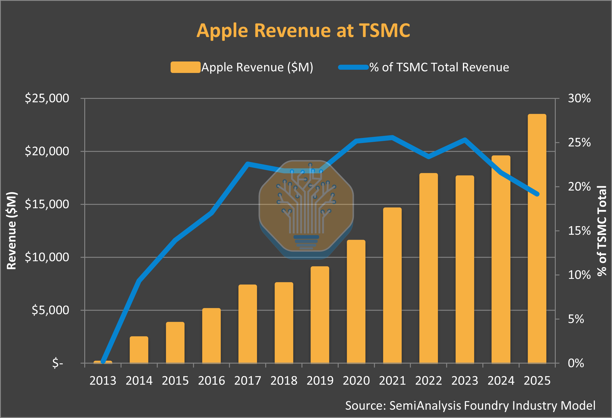
Apple’s annual spend at TSMC grew from $2B in 2014 to $24B in 2025. That is 12x in 12 years. Apple went from 9% of TSMC revenue to 25% at its peak and settled to 20% in 2025. More striking is Apple’s dominance at node launches: consistently >50% since 20nm and in some cases near 100%. Apple effectively funded the yield learning curve for every major node transition since 20nm.
The foundry model is dominant today. IDMs cannot support process development and fab capex with what is effectively a single customer. But even foundries need a “first and best” customer with large demand and deep pockets to fund their continued advance. Apple has been that customer for the last decade at TSMC. The juggernaut partnership has propelled both companies to new heights, put competitors in the dust, and fueled the chipmaking industry.
This report traces the Apple-TSMC relationship from Intel’s 2010 rejection through five distinct phases, examining how Apple built its chip empire through acquisitions and 8,000+ engineers across 15 design centers. We analyze why competitors have failed to replicate this vertical integration, map Apple’s manufacturing footprint across Fab 18 and advanced packaging facilities, and assess the strategic questions facing both companies as Intel 18A and Samsung re-engagement become viable alternatives. We’ll also discuss the next phase of the relationship. It’s not just Apple at the leading edge anymore. All of this is quantified with specifics from our proprietary Foundry Industry Model and Apple Wafer Demand Model.
Anchor Tenant
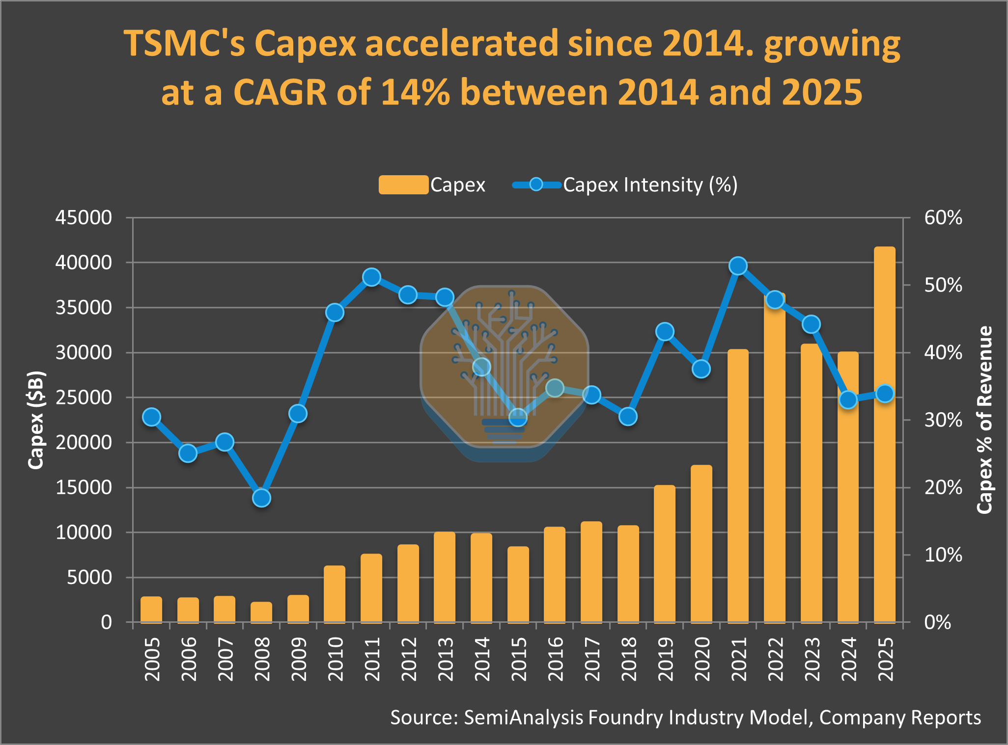
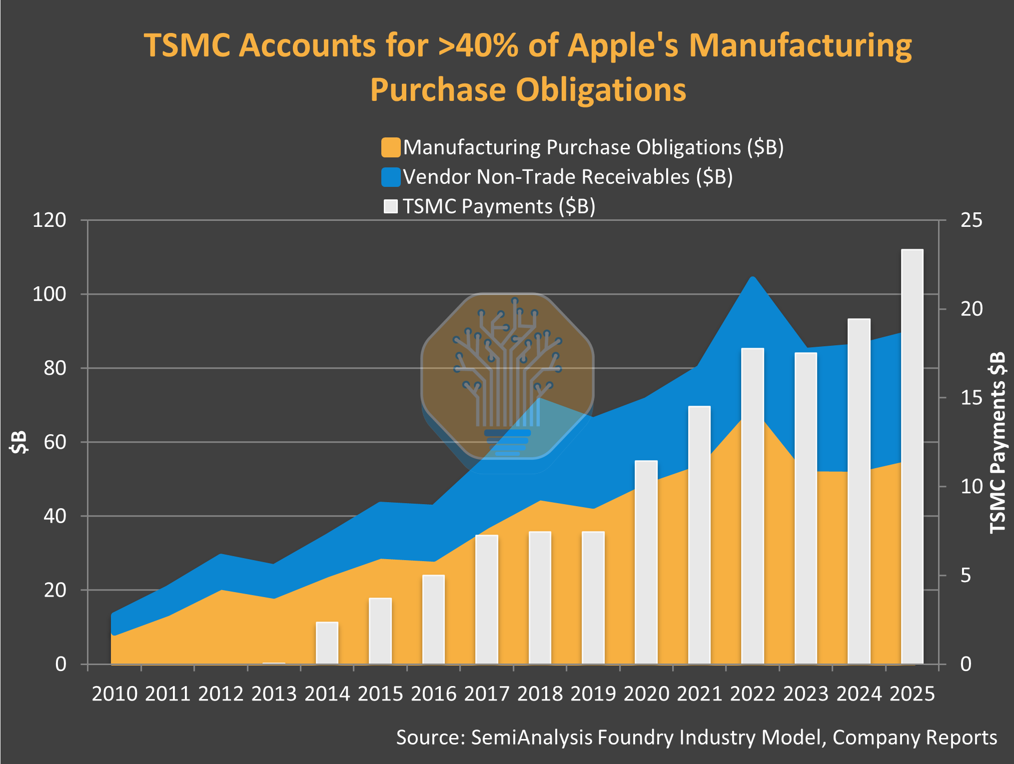
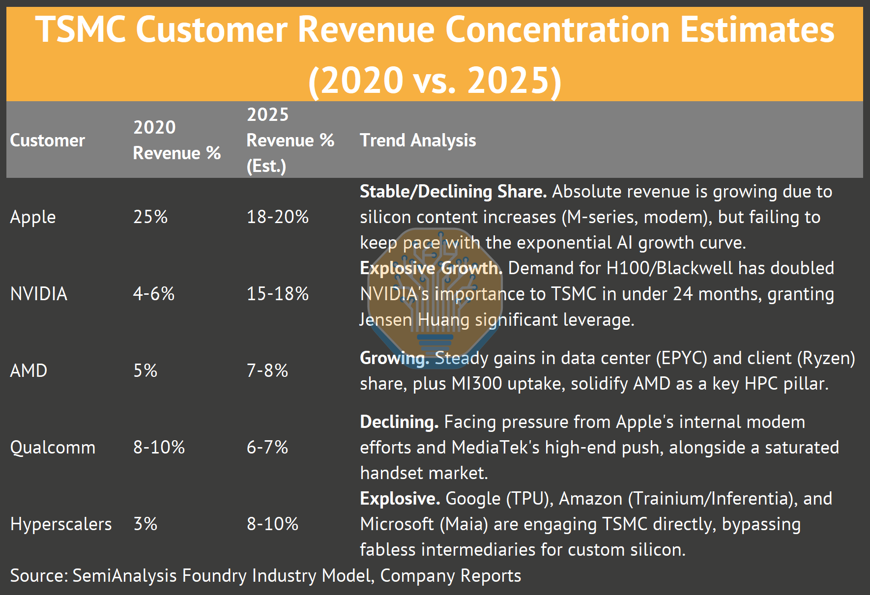
You can see the Apple effect in TSMC’s capex trajectory. Pre-Apple (2005-2009), annual spending averaged $2.4B with no anchor tenant to de-risk investment. From 2019-2022, TSMC deployed $98B, exceeding the cumulative spend of the prior 14 years. Apple’s manufacturing purchase obligations scaled from $8.7B in 2010 to $71B in 2022. TSMC-specific payments grew from near-zero in 2013 to $23B+ in 2025. For over a decade, Apple was the only company capable of pre-funding bleeding-edge capacity at scale. That changed with Nvidia’s AI-driven cash generation. Today, two companies can fund TSMC’s roadmap.
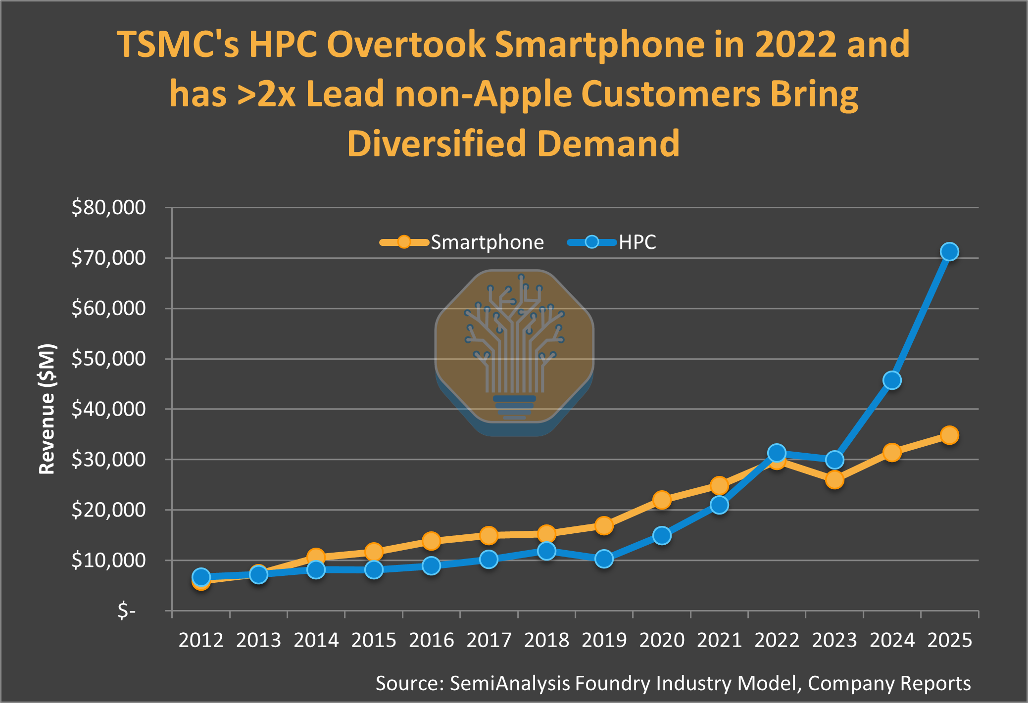
The platform shift has already happened. HPC revenue at TSMC grew from 36% in 2020 to 58% in 2025. Smartphone revenue shrunk to 29% from 46%. Our model shows Nvidia will consume more N3 wafers than Apple by 4Q27. Apple’s share of N2 drops to 48%, the first time in a decade Apple is not the dominant customer on a new node.
Consensus sees this as permanent displacement. Our model says otherwise.
TSMC’s A16 is architected for HPC. Backside power delivery, gate-all-around transistors, and thermal envelopes are optimized for HPC and smartphones will skip this node. Nvidia benefits disproportionately. Apple’s N2 (N2 + A16) share drops not because Apple lost leverage, but because the node was built for a different customer. A14 (1.4nm) rebalances the equation. TSMC is designing A14 for both mobile and HPC from the start, with a separate backside power (TSMC’s trade name is Super Power Rail) variant for HPC. Our model shows Apple reclaims 67% node share on A14, its highest since N3.
Apple is not standing still. New chip families (N-series, C-series) account for 15% of wafer demand by 2030. iPhone’s share of Apple’s wafer mix fell from 74% to 57% as Mac silicon and custom chips scaled. Gross margins reflect in-house silicon transition. Mac GM expanded from 28.5% to 39.5% after ditching Intel, an 11-percentage point expansion. iPhone GM grew 5 percentage points from A4 to A18. Annual chip savings exceed $7B across Intel, Qualcomm, and Broadcom displacement. Apple has driven $300B+ in supplier capex over the past decade, building a supply chain empire that spans Foxconn, ASML, and dozens of precision manufacturers.
What This Analysis Covers
The analysis is built on two proprietary models. Our Foundry Model tracks revenue, wafer shipments, and capacity allocation, quantifying the platform shift where smartphone revenue fell from 46% to 29% while HPC rose from 36% to 58%, and how Apple’s purchase obligations grew from $8.7B to $71B. Our Apple Wafer Demand Model forecasts silicon demand across chip families (A-series, M-series, S-series, N-series, C-series etc.), calculates gross margin savings exceeding $8B annually, and projects Apple’s leading-edge share declining from near 100% at N3 to <50% at N2 as AI accelerators reshape allocation. The report concludes with Taiwan risk scenarios, Arizona economics, and conditions under which Apple would build its own fabs.
Key Numbers
Wafer Demand
· A-series: $4.2B (2018) to $9.7B (2025) = 131% growth
· M-series: $0 (2019) to $4.9B (2025) = From zero to $5B in 6 years
· S-series: $86M (2018) to $342M (2025) = 4x growth
· Total Apple Silicon Revenue: $23.5B (2025)
TSMC Transformation:
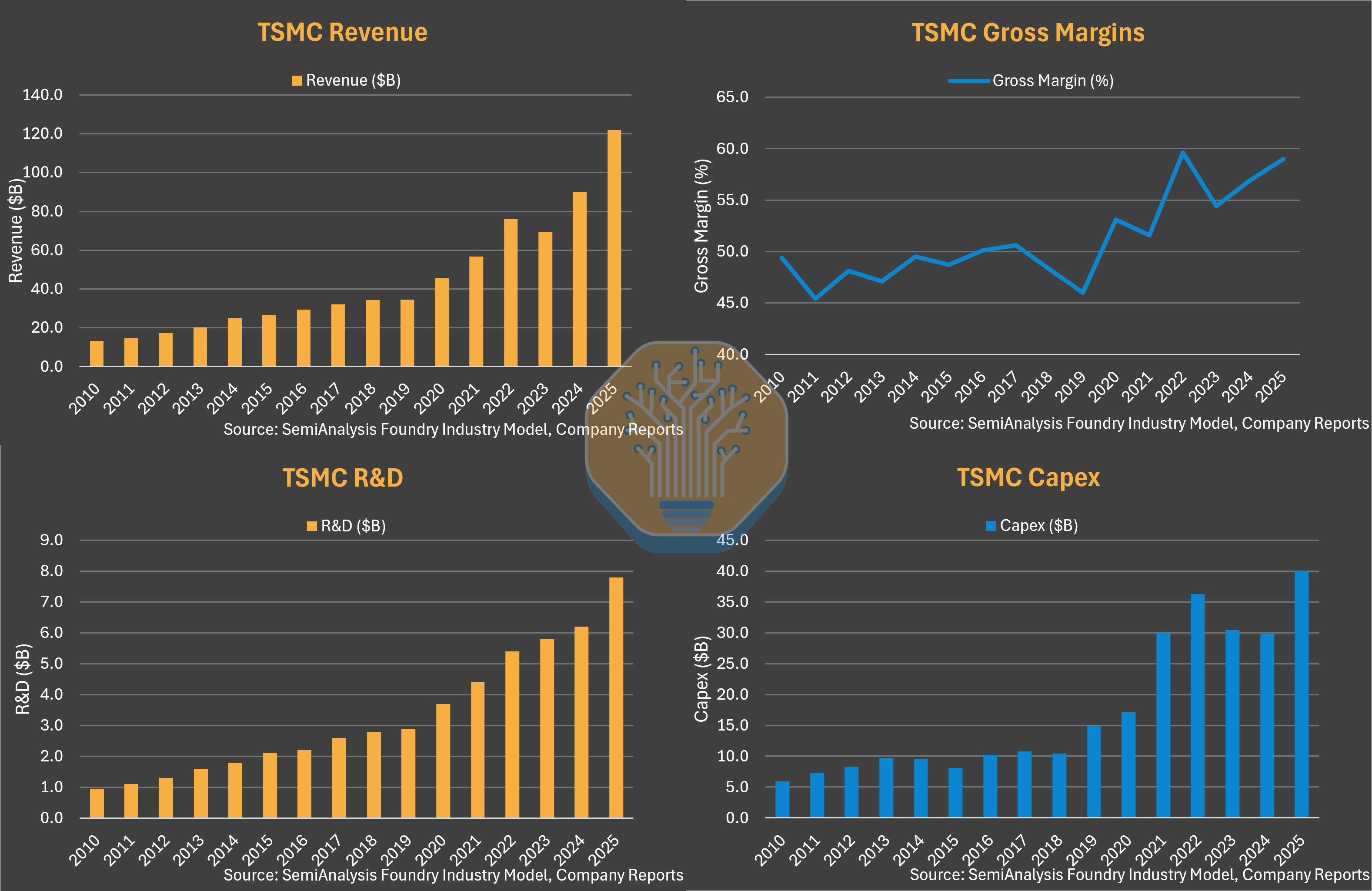
· Revenue: $13B (2010) to $122B (2025) = 9.4x growth
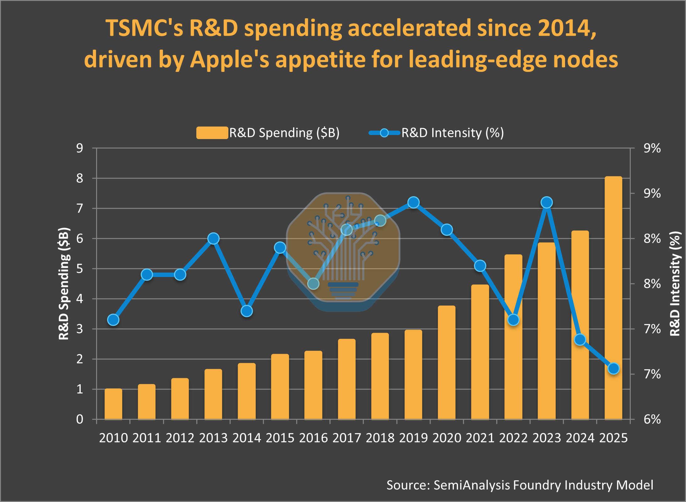
· R&D: $1B (2010) to $8B+ (2025) = 8x growth
· Capex: $5.9B (2010) to $41.4B+ (2025) = 7x growth
· Gross Margin: 45.5% (2010) to 59%+ (2025) = 13.5pp expansion
The Packaging Revolution:
· CoWoS Revenue: $0.6B (2018) to $8.4B (2025) = 14x growth
· Apple InFO Revenue: $3.5B+ (2025)
· TSMC Advanced Packaging as % of Revenue: 6-7% (2018) to 10%+ (2025)
Apple’s Supply Chain Leverage:
· Manufacturing Purchase Obligations: $8.7B (2010) to $56.2B (2025) = 6.4x growth
· Monthly Wafer Demand: 19K (2013) to 130k (2025) = 7x growth
· Fab 18 Customers: 4 (2020) to 45 (2025) = 11x growth
Chip Economics:
· iPhone Gross Margin: 36.5% (A4, 2018) to 41.5% (A18, 2025) = 5pp expansion
· Mac Gross Margin: 29% (Intel, 2019) to 39.5% (M3 Pro, 2023) = 10.5pp expansion
· Annual Chip Savings: $7B+ (Intel $5B + Qualcomm $1.2B + Broadcom $700M + custom IP $500M+)
Platform Shift at TSMC:
· Smartphone Revenue %: 46% (Q1 2028) to 29% (Q4 2025)
· HPC Revenue %: 36% (Q1 2020) to 58% (Q4 2025) = HPC now dominates
The Five Phases of Apple-TSMC Evolution
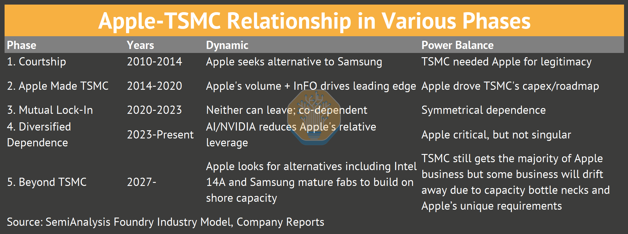
Phase 1: Why Apple started making its own chips and Apple’s courtship
The original iPhone launched in 2007 relied heavily on Samsung components. Samsung supplied the application processor, display, and flash memory. While making its chips an inevitable destiny for Apple, a few things accelerated the journey.
First, Apple’s key supplier Samsung entered smartphones 18 months after iPhone launched, ending up in a legal battle with Apple as early Galaxy S designs resembled iPhones. The unease grew with each Samsung’s release and its growing competitive position smartphones, pushing Apple to look for alternatives.
Second, the rise of the Wintel model (Android plus Qualcomm) in smartphones in the 2010s worried Apple that commodity chips could erode its differentiation in software and affect its premium status. Jobs made the call in 2008: Apple would design its own chips. But manufacturing requires 10s of billions in fabs. So Apple adopted a fabless systems company approach.
Third, workload optimization: designing for iOS specifically, rather than generic benchmarks, enabled meaningful performance-per-watt advantages.
Fourth, power efficiency: iPhone’s thin form factor demanded performance-per-watt leadership that merchant silicon couldn’t deliver.
Fifth, margins: eliminating supplier markups over time would capture billions in additional profit.
Apple wanted to control the primary technologies used in its devices. The $278M P.A. Semi acquisition in April 2008 served as a stepping stone. Dan Dobberpuhl, creator of Alpha and StrongARM, had assembled 150 of the best low-power chip engineers in the world. Among them was Johny Srouji, an Israeli engineer from Intel and IBM. He now runs Apple Silicon as SVP of Hardware Technologies.
First and foremost, if we do this, can we deliver better products? That’s the No. 1 question. It’s not about the chip. Apple is not a chip company.
- Johny Srouji, Apple SVP of Hardware Technologies
Following P.A. Semi, Apple acquired ultra-low-power chip design company Intrinsity for $121M in 2010 Apple fielded its first custom smartphone applications processor (AP), the A4, in iPhone 4 in September 2010. While it was still manufactured by Samsung, Apple intensified its search for a manufacturing partner who wasn’t also their competitor.
The Decision That Changed Computing History: TSMC vs Samsung vs Intel Decision
Between 2010 and 2014, the “courtship” phase, Apple explored alternatives to Samsung via “Project Azalea,” considering GlobalFoundries and even building its own fabs.
Enter Intel and TSMC, two of the leading fab options for Apple. Discussions with Intel were unsuccessful as then CEO Paul Otellini declined, believing the volume wouldn’t justify the low margin and rigorous demands Apple placed on suppliers. At TSMC, Morris Chang accepted the challenge, viewing it as a growth opportunity rather than a margin drag.
Apple COO Jeff Williams met with Chang over dinner and pitched TSMC to build 20nm capacity. At that time, TSMC was shifting focus and investment to 16nm. The capital and capacity numbers Apple asked were unheard of; they went so far as suggesting TSMC cut its dividend to fund the fab buildout. TSMC made the bet. They were able to fund the fabs with debt. At the time of the initial decision, success was far from a sure thing for either side.
Phase 2: Apple Made TSMC (2014-2020)
Apple’s A8 chip launched in 2014, and TSMC never looked back. Over the next six years, Apple drove TSMC to invest $60-80 billion in leading-edge capacity. Apple’s volume justified every major node transition: N16, N7, N5. Without the iPhone’s annual 200M unit baseline, TSMC could not have afforded the R&D velocity that left Intel and Samsung behind.
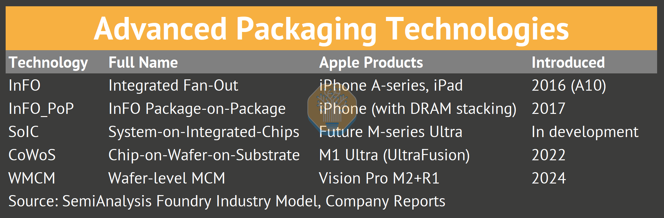
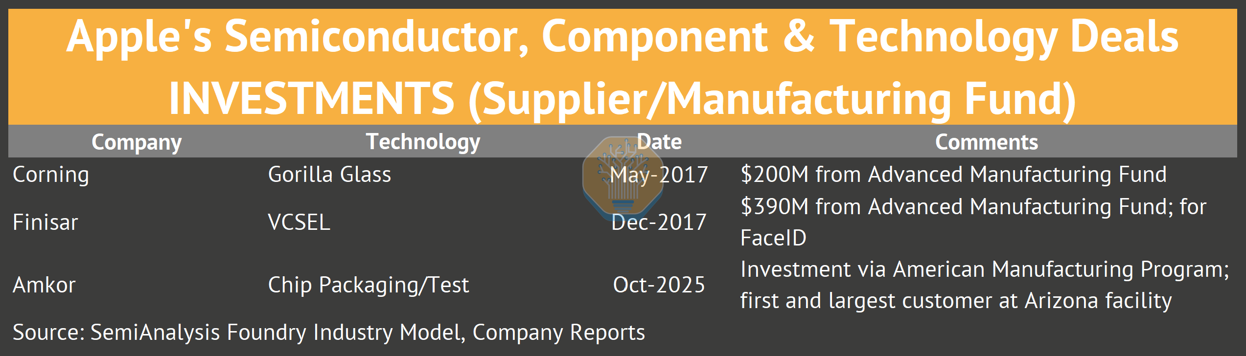
In 2016, Apple funded the development of InFO (Integrated Fan-Out) packaging. This allowed for thinner phones with better thermals and created the advanced packaging ecosystem that now powers AI accelerators.
In a candid interview, Morris Chang revealed that Tim Cook later told him:
Intel just does not know how to be a foundry.
At the core there are cultural differences: Intel, trapped in its product success, couldn’t foresee the massive Arm-based foundry market; TSMC offered servitude, flexibility, and a willingness to ‘bet the company’ on Apple’s success. TSMC built dedicated capacity, accepted Apple’s engineers into their labs, and aligned their roadmap with the iPhone’s annual cycle. This cultural alignment, TSMC’s willingness to customize versus Intel’s standardized product approach, remains Intel’s biggest hurdle in its IDM 2.0 pivot today.
Apple initially said to have offered 40% gross margin to TSMC, which was in line with TSMC’s margin then. Current gross margin from Apple business is significantly higher than the initial 40%.
Despite investing in dedicated 20nm capacity for Apple, TSMC did not even receive a majority share of Apple’s foundry business at first. It had to share a 14nm slot with Samsung in 2015 with the latter getting >60% share. TSMC management was shocked, but responded by accelerating their next-gen 10nm process.
Ultimately, TSMC won because it demonstrated the ability to scale 20nm ahead of the competition, proving it could handle the iPhone’s massive volume spikes. The “Night Hawk” team at TSMC worked 24/7 to solve yield issues, establishing the operational trust that persists today.
What if Apple chose Intel in 2014? Intel would have $15B+/year guaranteed foundry revenue. TSMC, without that revenue, would probably not have achieved dominance anywhere near what it has today. Intel Foundry would be 10 years more mature. It’s the biggest misstep in the history of chip foundries.
Phase 3: Mutual Lock-In (2020-2023)
By 2020, the partnership had evolved from mutually beneficial to co-dependence. Apple could no longer leave. No other foundry on earth could produce M-series and A-series chips at the required volume and yield. Samsung’s 3nm yields were 30-40% versus TSMC’s 80%+. The switching cost was estimated at $2-5 billion in redesign and requalification alone.
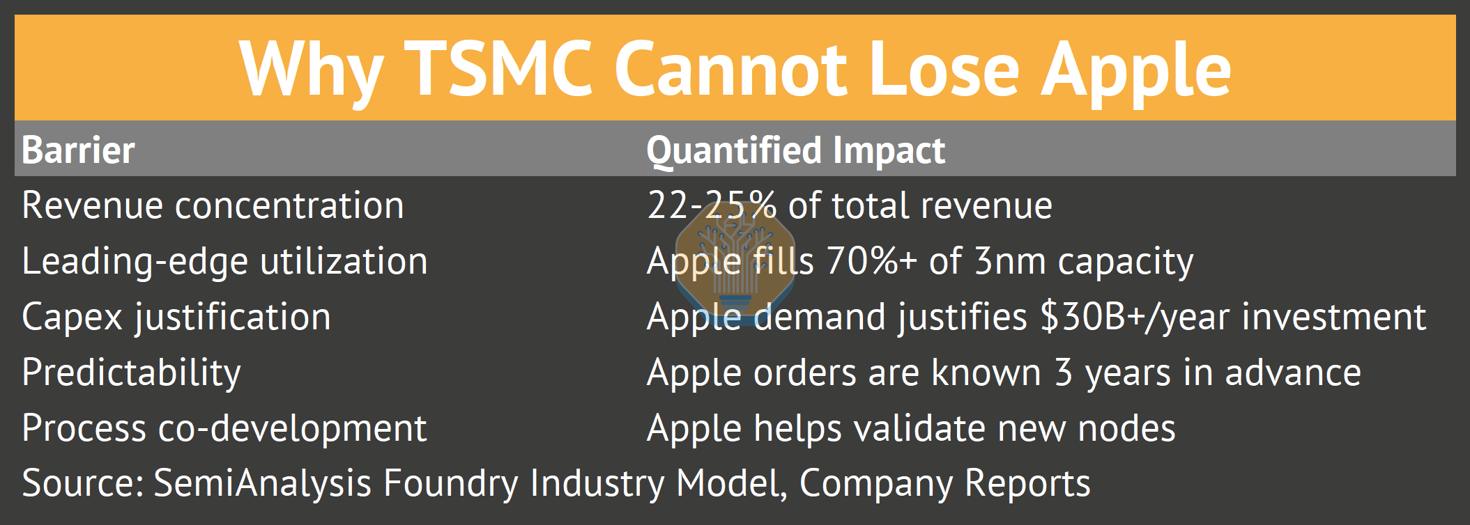
TSMC could not lose Apple. The iPhone brought 22-25% of total revenue and filled 70%+ of 3nm capacity. Apple orders were known three years in advance, allowing TSMC to plan capex with the confidence of a utility company.
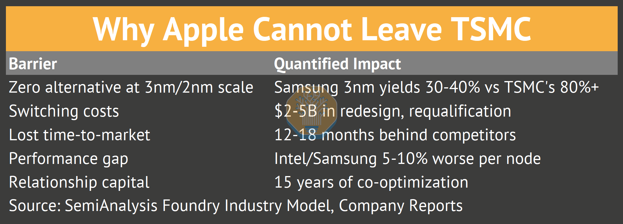
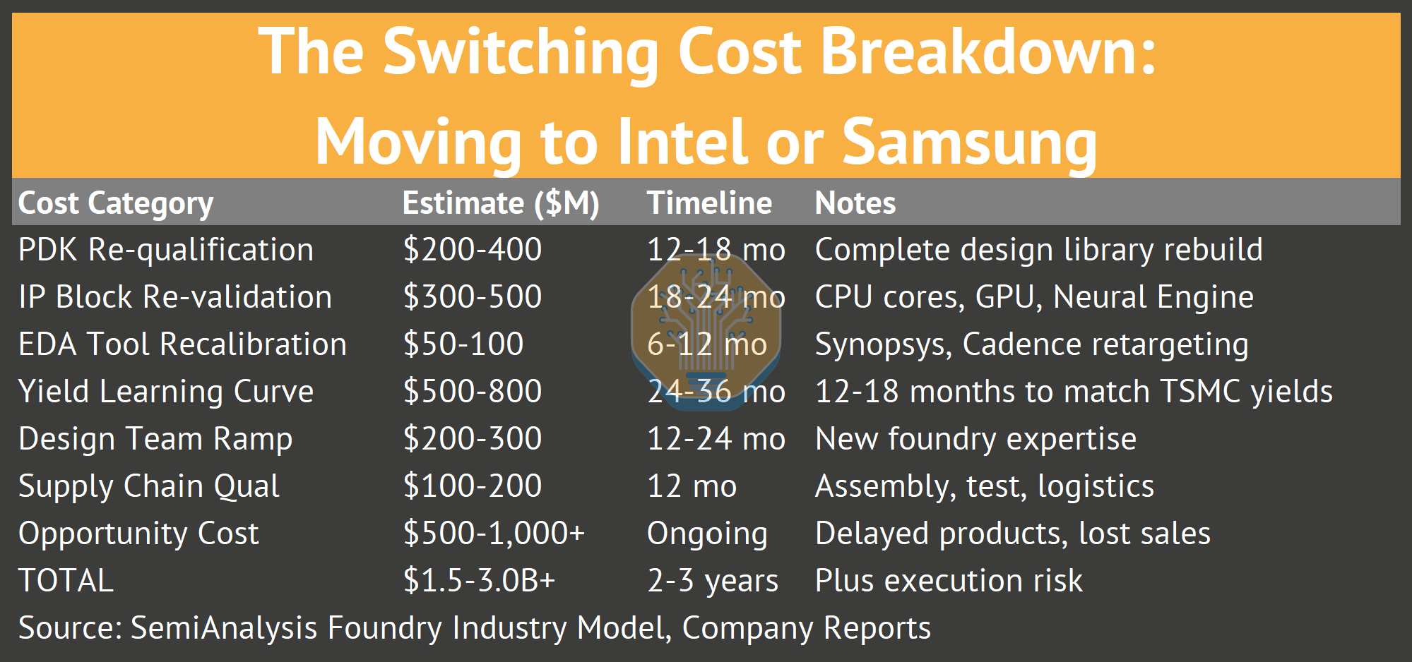
A more serious risk is timing. Apple’s product cadence is synchronized to TSMC’s node roadmap. Moving to Intel or Samsung would mean 2-3 years of inferior products while yield learning catches up. Product upgrade cycles, most importantly the annual iPhone refresh synced with holidays, would also be at risk.
Phase 4: Diversified Dependence (2023-Present): The Changing Power Dynamic: Is Apple Still the Kingmaker?
For years, Hsinchu and Cupertino worked as a single team to relentlessly advance Moore’s Law. Apple’s One Team approach embedded hundreds of engineers at TSMC’s headquarters, effectively treating the foundry as an extension of Cupertino. This team co-developed Process Design Kits (PDKs), ensuring that when a new node like 5nm launched, Apple’s designs were perfectly synthesized to the transistor characteristics.
However, the rise of generative AI is shifting TSMC’s customer mix. While Apple remains the largest single customer by revenue, its relative influence is diluting as the High-Performance Computing (HPC) segment, driven by NVIDIA, AMD, and hyperscalers, outgrows. In Q1 2020, smartphones accounted for 49% of TSMC’s revenue, while HPC was 30%. By Q3 2025, HPC had skyrocketed to 57%, relegating smartphones to a secondary growth driver.
While Apple also contributes to TSMC’s HPC segment through its tablet/PC chips, the uptake of AI offered TSMC a new stream of customers who are voracious for advanced node capacity. While AI accelerators moved 1 year cadence, they are still on n-1 node largely. Apple will still be the anchor customer on N2 (2nm) but it will see stiff competition from others competing for capacity. On A16 (1.6nm), HPC players are likely to beat Apple as it is a more HPC centric node.
Apple acts as the predictable baseline that justifies the massive, fixed costs of new fabs. NVIDIA provides the high-margin upside that drives profitability growth. TSMC now has two anchor tenants instead of one.
The AI Divergence: Wafers vs. Packaging
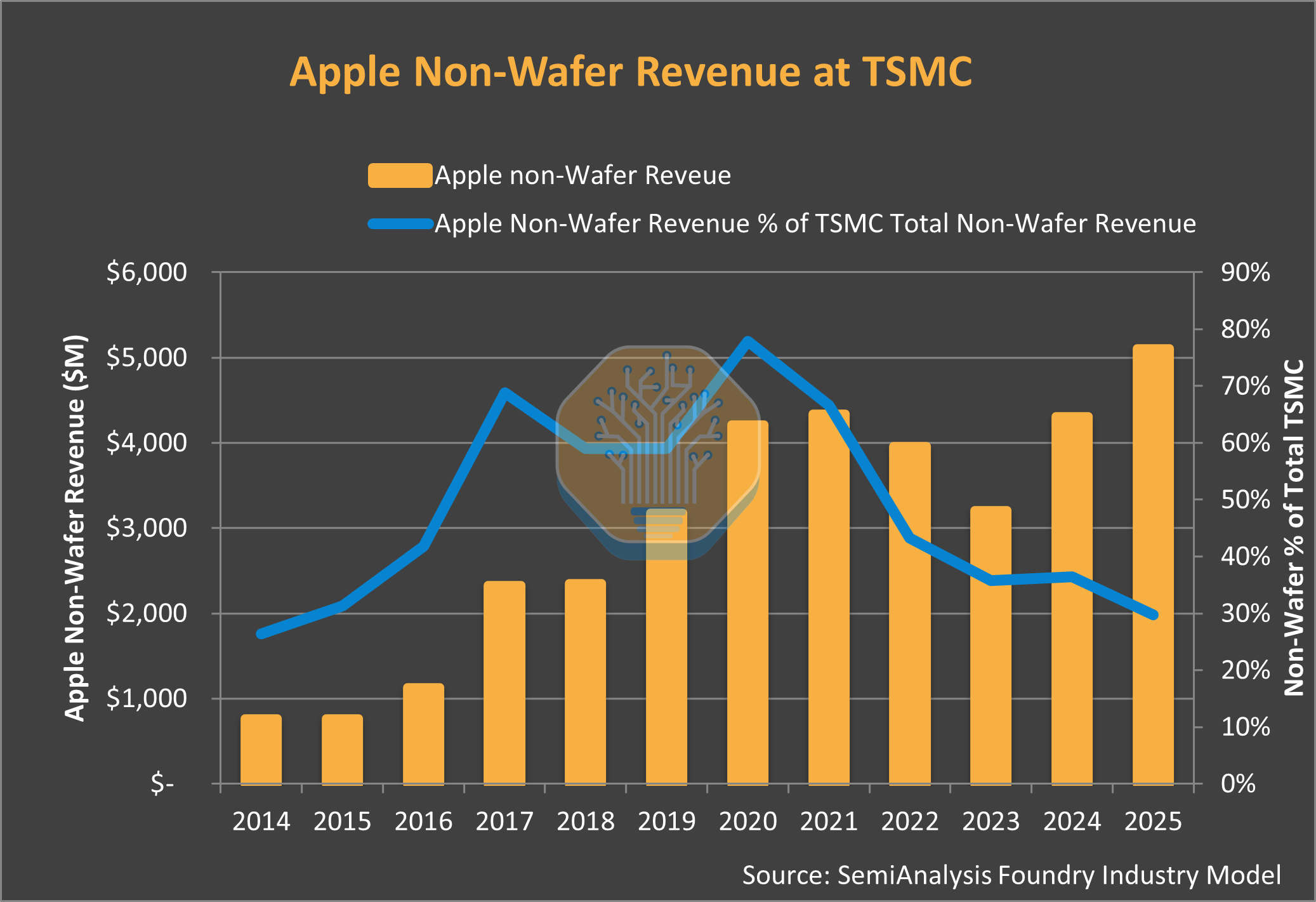
The distinction lies in what these customers are buying. Apple buys leading-edge logic wafers (N3, N3E) and InFO (Integrated Fan-Out) packaging. NVIDIA buys logic wafers (N4, N5) on a custom process a node or 2 behind leading edge but is critically dependent on CoWoS (Chip-on-Wafer-on-Substrate) packaging.
Apple was TSMC’s first advanced packaging customer at scale. InFO revenue grew from $1.8B in 2018 to >$3.5B in 2024, driven entirely by A-series and M-series chips. But CoWoS, TSMC’s AI packaging platform, has surpassed it. CoWoS revenue hit $9.6B in 2025, 2.5x InFO, fueled by Nvidia and AMD demand.
This creates a bifurcation in TSMC’s capacity planning. Apple is no longer the sole driver of capex. TSMC’s capital expenditure is now split between chasing Moore’s Law (2nm for Apple) and chasing packaging density (CoWoS-L for NVIDIA). Apple acts as the predictable baseline that justifies the massive fixed costs of new fabs, while NVIDIA provides the high-margin upside that drives profitability growth. The power dynamic has shifted from a unipolar world (Apple) to a bipolar world (Apple + AI), where TSMC can now arbitrage demand between the two sectors to maintain pricing power.
Phase 5: Beyond TSMC (2027+)
Apple is actively exploring alternatives.
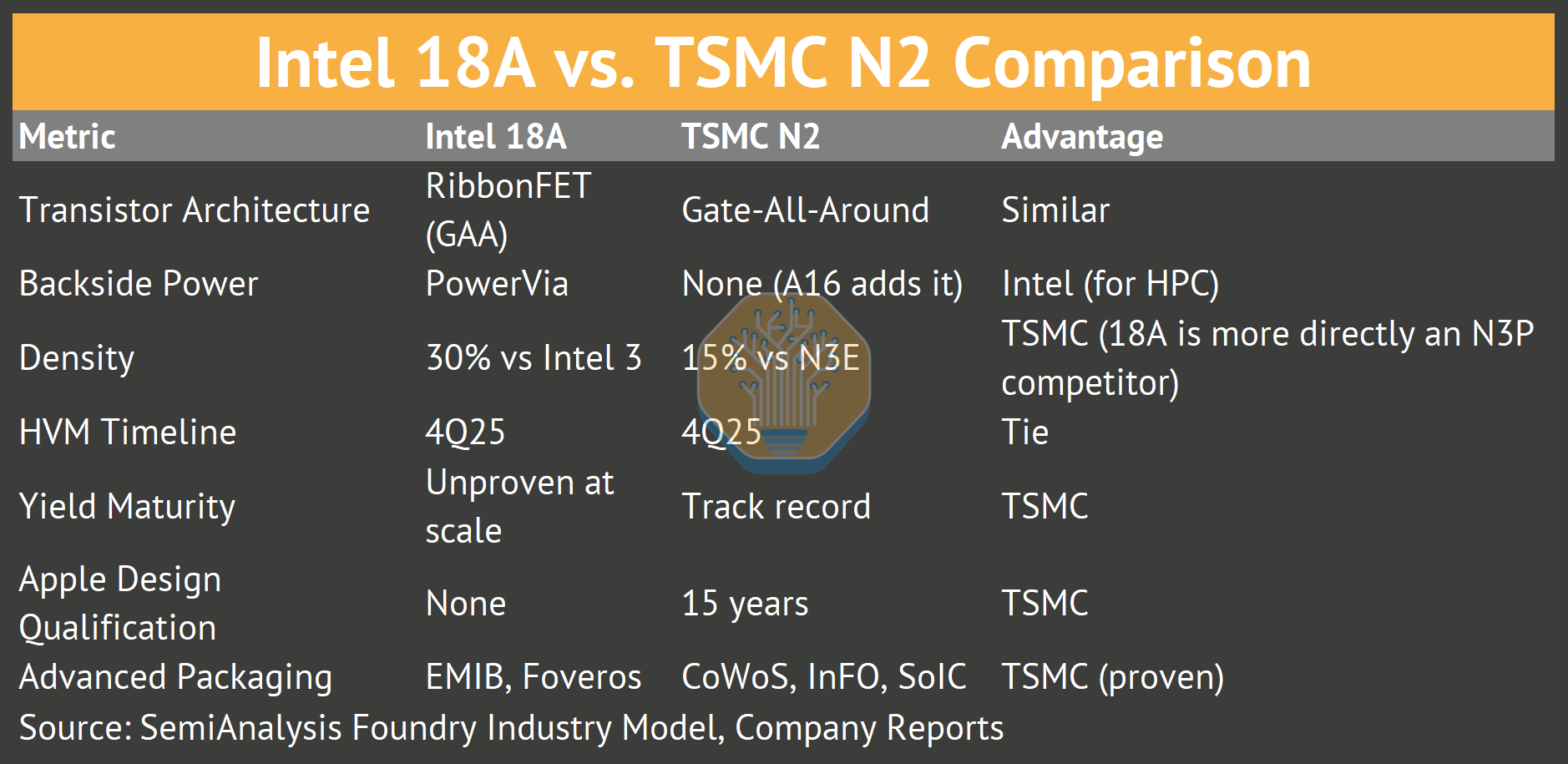
Intel’s 18A-P process (shipping late 2026) represents the first theoretically viable alternative since Apple left Samsung in 2016. Apple could qualify Intel, initially for lower-risk silicon such as base M-series, and yield well. That would give Intel reference design wins and Apple supply chain diversification without risking core products.
Intel missed Apple once before in 2014. The door hasn’t fully closed. The key question is: would Apple actually use it?
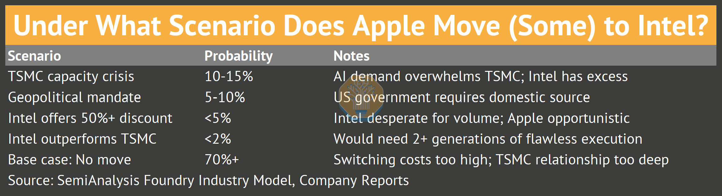
But, 18A-P on base M-series chips makes sense. If Apple were to shift 20% of base M-series wafers to Intel 18A-P, it would imply $630M in foundry revenue for Intel at an $18k ASP.
Base M-series die sizes tend to be in the range of 150-170mm² and could yield 70%+ on 18A-P (based on current Panther Lake, which has a similar die size).
While Intel’s current 18A yields are lower than TSMC’s N3 for a 150mm² die (>80%), Intel offers pricing leverage, potential 14A optionality, and US-based wafer/packaging capabilities for Apple.
Intel 18A-P offers 8% higher performance/watt and similar density to 18A with backside power delivery (PowerVia).
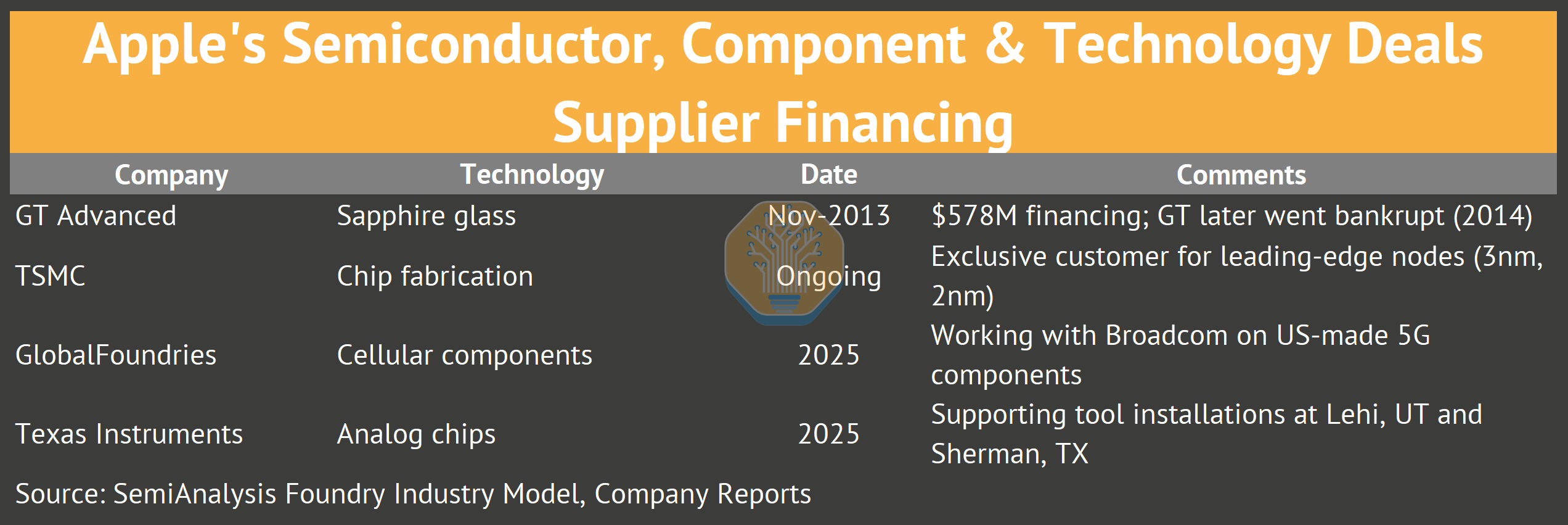
There are a few lower impact possibilities too: while the Intel16 mature node in its Ireland fab could address DTV and connectivity apps, we doubt the capacity is enough to serve Apple. Apple could qualify Intel for lower-risk silicon: WiFi/Bluetooth, display drivers, or power management. That would give Intel reference design wins and Apple supply chain diversification without risking core products.
Apple’s Real Diversification Strategy
Apple’s actual foundry diversification isn’t about moving leading-edge A-series/M-series away from TSMC. Non-Pro versions, Peripheral chips and packaging are all candidates for foundry diversification.
Where diversification makes sense: PMICs, Display Drivers, Audio/Connectivity
Where diversification is Challenge: leading-edge A-series and M-series
Apple’s Reengagement with Samsung LSI/Foundry
After leaving Samsung in 2016, Apple went exclusive with TSMC. Apple’s diversification strategy is about reducing supply chain risk for non-critical chips.
Apple has signed a strategic deal with Samsung Foundry to manufacture advanced CMOS Image Sensors (CIS) at Samsung’s Austin, Texas facilities, breaking Sony’s decade-long exclusivity on iPhone image sensors. Leveraging Samsung’s US fabs helps Apple meet internal “American Manufacturing” targets without relying solely on TSMC Arizona, which is focused on leading-edge.
We estimate Samsung could capture 20-30% of Apple’s CIS volume by 2027 (150M-200M sensors annually), offering $1-$1.5B foundry revenue to Samsung.
The Manufacturing Footprint
Mapping the Apple-TSMC Ecosystem: Where the Silicon is Born
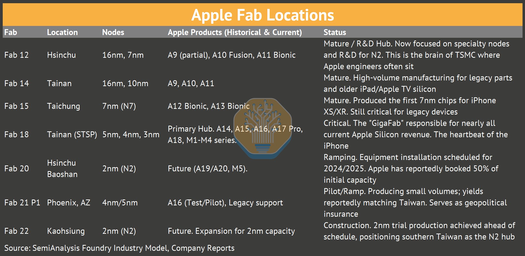
To understand the relationship, one must understand the physical reality of where these chips are made. TSMC’s dispersed network of GigaFabs, each specializing in specific nodes and packaging technologies, churn out over a billion chips for Apple each year. Apple’s supply chain is deeply entrenched in Taiwan’s western corridor, but geopolitical hedging is forcing a costly expansion to Arizona.
The Critical Back-End: Advanced Packaging
Advanced packaging is an area where the divergence between Apple and NVIDIA is most acute. Apple relies on InFO-PoP (Integrated Fan-Out Package-on-Package), which stacks DRAM directly on top of the SoC to minimize thickness for iPhones. This technology was pivotal in Apple’s decision to leave Samsung, as it allowed for thinner phones with better thermal dissipation. NVIDIA, on the other hand, relies on CoWoS, which places HBM (High Bandwidth Memory) side-by-side with the GPU on a silicon interposer for maximum bandwidth.
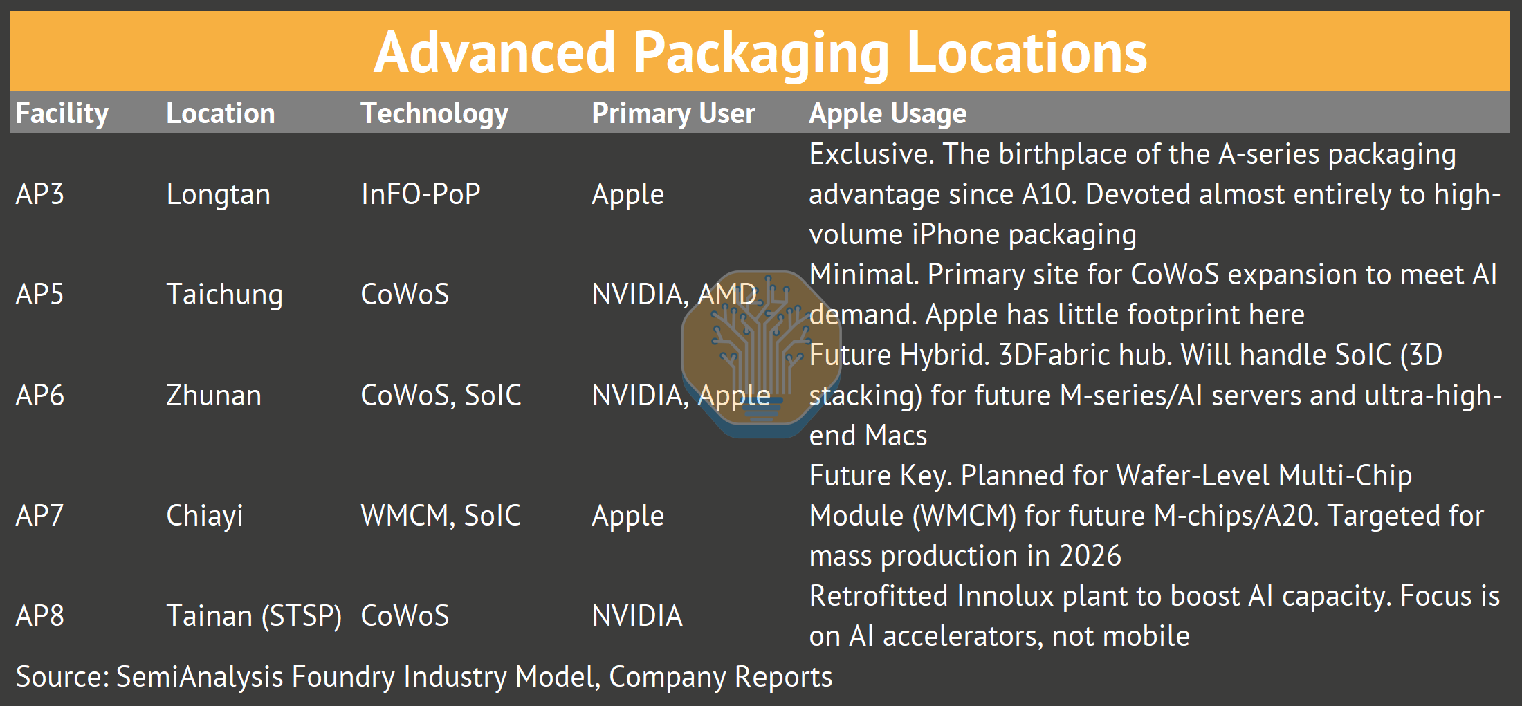
Apple and NVIDIA do not compete for the same packaging lines today. Apple dominates AP3 (InFO), while NVIDIA fights for AP5/AP6 (CoWoS). However, as Apple moves toward M5/M6 Ultra chips utilizing SoIC (System on Integrated Chips) and WMCM, they will begin to compete for the same advanced 3D packaging resources in AP6 and AP7. This convergence of roadmaps poses a future risk for capacity allocation.
Fab 18 in Tainan is TSMC’s flagship facility for leading-edge production and it’s essentially “Apple’s fab.” The A19 Pro, A18 Pro, M3, M4 and M5 all come from Fab 18’s 3nm lines. This concentration in southern Taiwan is one of the key geopolitical vulnerabilities in Apple’s supply chain.
Geographic Concentration Risk
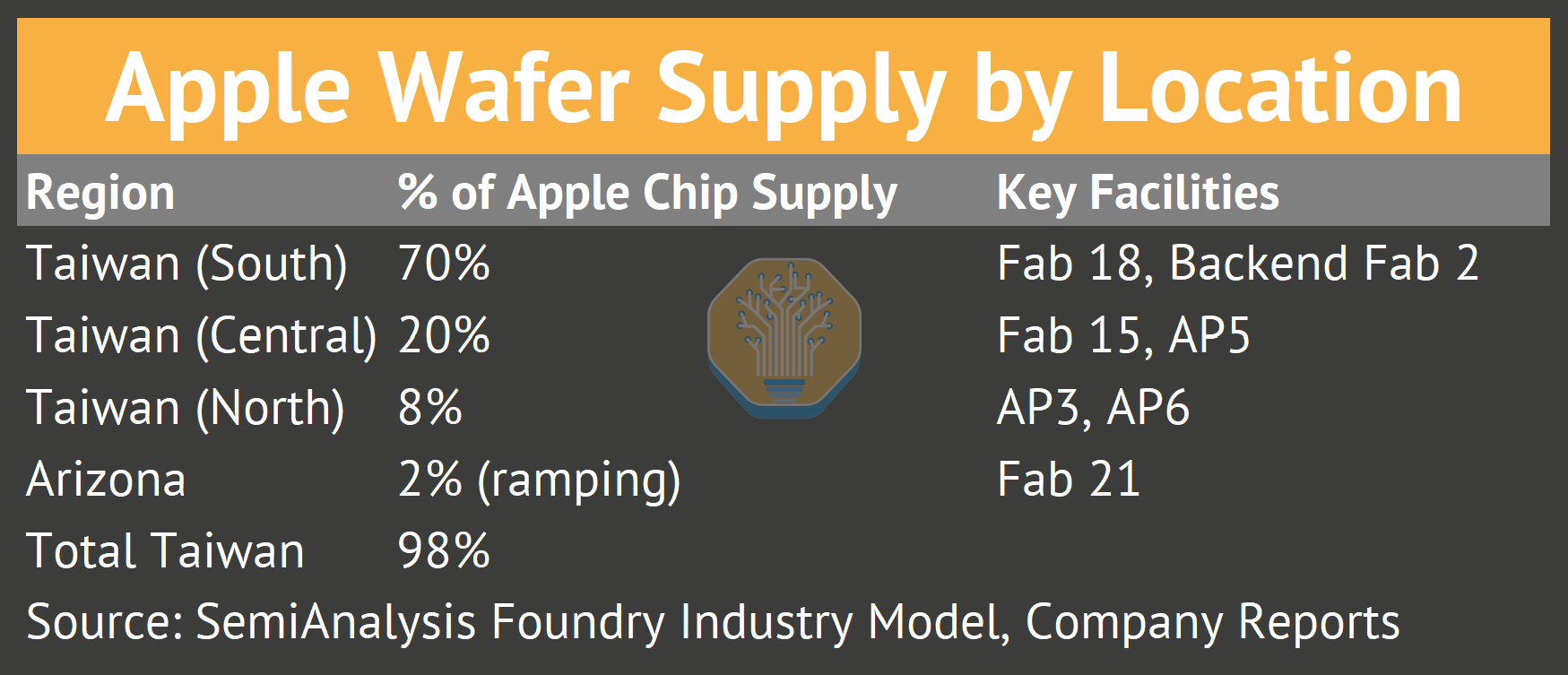
Apple’s Taiwan concentration is the elephant in the room. Nearly all of Apple’s chip production, including every leading-edge A-series and M-series chip, happens on a single island 100 miles from mainland China.
TSMC Arizona provides token diversification, but at current ramp rates, it won’t materially reduce Taiwan dependence until 2028+. Currently <5% of leading-edge production is from Arizona. If this rises to 10-15% by 2028, it signals Apple is genuinely worried about Taiwan.
Apple’s Five Transformational Chip Acquisitions
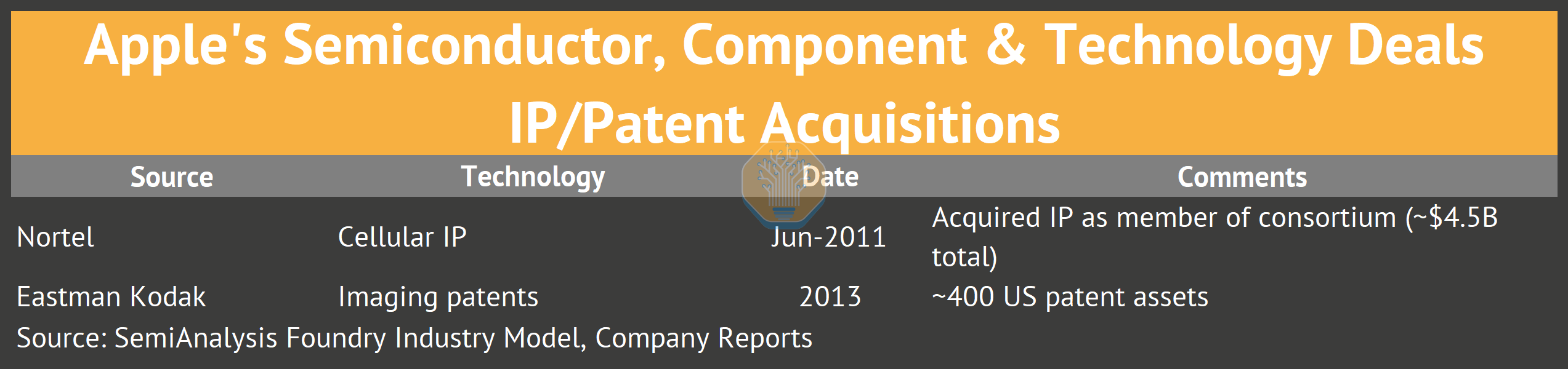
Apple’s overarching semiconductor philosophy is simple but ruthless: control the “primary technologies” that differentiate the product. This journey, which began with the A4 in 2010, has evolved into a comprehensive internalization strategy. It’s not just about the CPU (A-series/M-series); Apple has systematically replaced suppliers for almost every critical subsystem, developing custom silicon for Audio (H-series), Security (T-series), Wireless (W-series), Ultra-Wideband (U-series), and now Spatial Computing (R-series). The acquisition of Intel’s modem business in 2019 was the final piece of this puzzle, aiming to displace Qualcomm and complete the complete silicon independence.
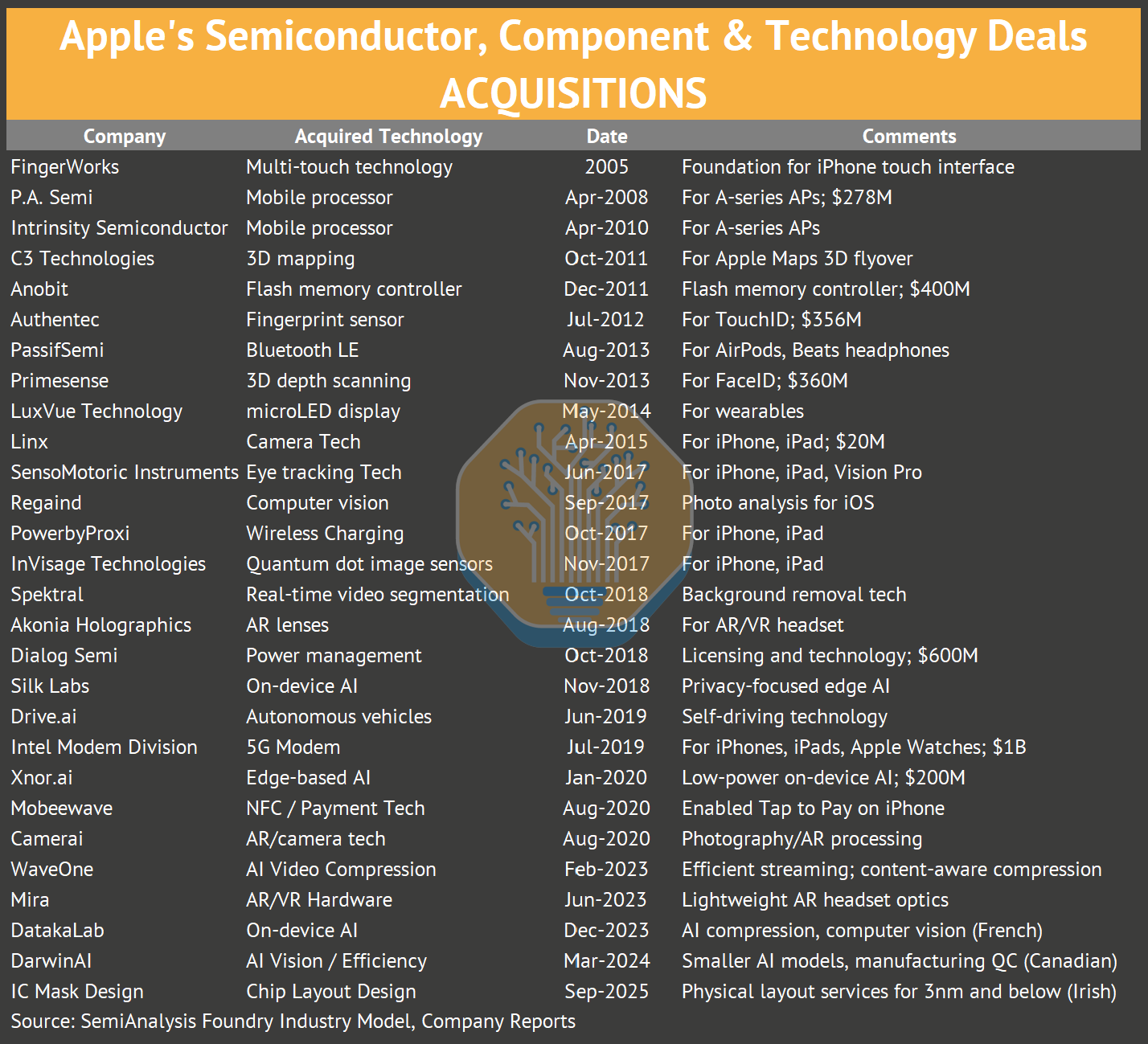
P.A. Semi (2008, $278M): The Foundation
P.A. Semi was a boutique chip design firm founded by Dan Dobberpuhl, one of the most respected processor architects in the industry (creator of DEC Alpha, StrongARM). The company had 150 engineers designing low-power, high-performance processors.
The team designed the A4, Apple’s first custom SoC. Jim Keller, who later designed AMD’s Zen architecture, led the A4/A5 development at Apple before departing.
AuthenTec (2012, $356M): Touch ID
Touch ID launched 13 months after the AuthenTec acquisition. AuthenTec’s architecture enabled the Secure Enclave, the hardware security subsystem that handles all biometric and cryptographic operations.
The Secure Enclave enabled Apple Pay (2014). A decade on, Apple Pay enabled $1.5T+ in transaction volume (2024). The $356M acquisition justified a financial services business that generates billions in annual revenue. A chip architecture decision in 2012 enabled a $100B+ Services business a decade later.
PrimeSense (2013, $360M): Face ID
PrimeSense developed the 3D depth-sensing technology behind Microsoft’s Kinect. Apple bought them for $360M and spent four years miniaturizing the technology to fit in a phone notch.
The TrueDepth camera projects 30,000 infrared dots onto your face, maps the 3D structure, and authenticates in milliseconds. Face ID is more secure than Touch ID (1 in 1,000,000 false positive rate vs. 1 in 50,000).
The same technology enabled Animoji, Memoji, and became the foundation for LiDAR Scanner in the iPhone 12 Pro.
Intel Modem Business (2019, $1B): In-house 5G Modem
Apple bought Intel’s smartphone modem business the same week they settled their lawsuit with Qualcomm. The timing was intentional. The settlement was a temporary truce.
With Intel, Apple acquired 2,200 engineers (modem design, RF, validation), 17,000 wireless patents, Labs, equipment, IP across San Diego and Munich
The 5G modem was the final frontier for Apple and despite delays, the C1 modem shipped in iPhone 16e (2025), after five years of development. By 2027-2028, Apple expects to eliminate Qualcomm entirely in its lineup, offering it a gross margin stacking opportunity.
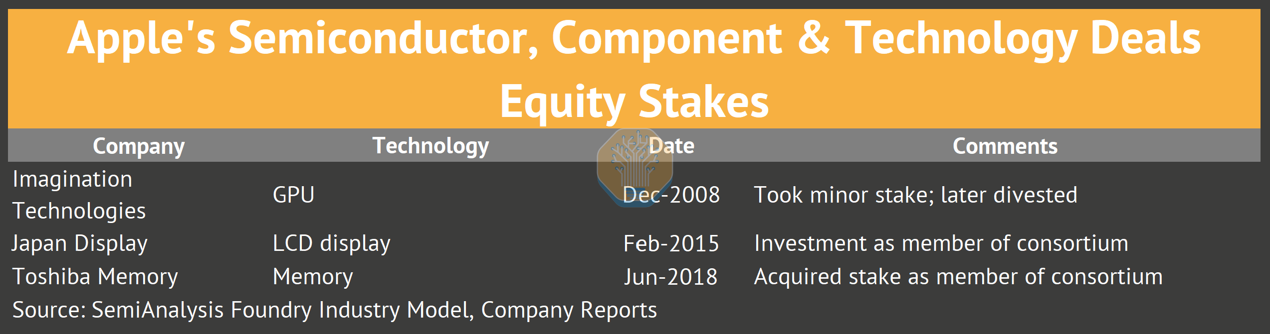
The Imagination Breakup (2017): In-House GPU
Apple has licensed GPU designs from Imagination Technologies since the original iPhone. In April 2017, Apple notified Imagination they would stop using their IP within 15-24 months. Imagination’s stock dropped 70% overnight.
Apple had secretly built an internal GPU team. The A11 (September 2017) shipped with Apple’s first custom GPU. The Apple GPU delivered 30% better performance than Imagination’s designs.
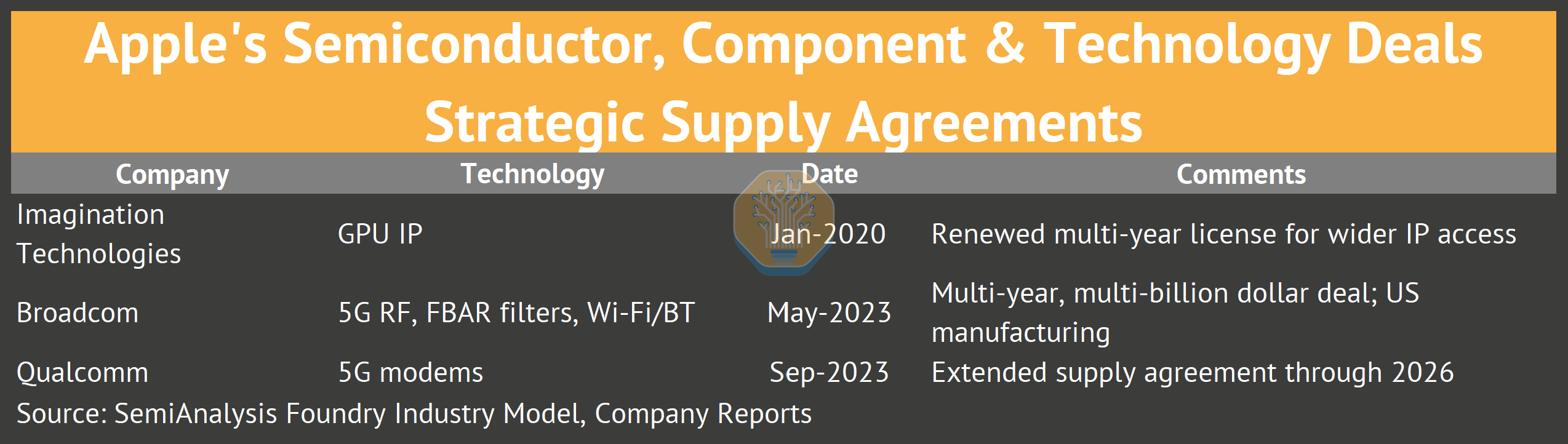
Imagination nearly went bankrupt. They were sold to a Chinese-backed private equity firm. By 2020, both companies settled their disputes and entered into multi-year licensing agreements.
Global Design Operations
Apple operates 8,000+ chip engineers across 15+ design centers on four continents:
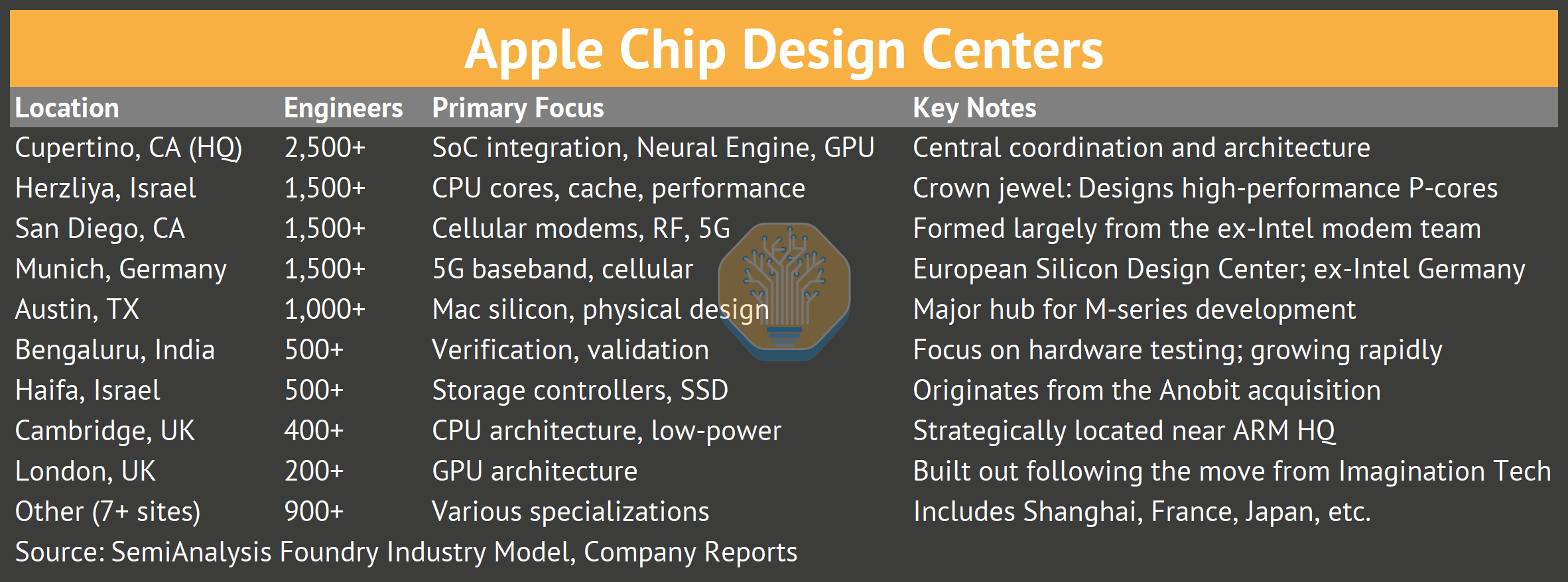
Israel is where Apple’s CPU performance leadership is designed. The Herzliya team, many recruited from Intel Israel, which created Pentium M, Core, and Sandy Bridge architectures, designs the Firestorm, Avalanche, and Everest cores that dominate benchmarks.
The same country that gave Intel its best architectures now designs Apple chips that beat Intel.
The San Diego facility is squarely targeted at Qualcomm. Apple’s modem design operation sits literally down the street from Qualcomm’s headquarters. The office is staffed largely with ex-Qualcomm and ex-Intel engineers, people who know exactly how Qualcomm’s modems work and how to beat them.
DTCO: Design-Technology Co-Optimization
Apple co-defines the Process Design Kit (PDK) with TSMC. TSMC effectively dedicates hundreds of engineers to Apple, creating what is essentially a “virtual IDM” (Integrated Device Manufacturer). When Apple dictates a need for wider memory buses or specific transistor architectures, TSMC adjusts the PDK to match.
Silicon Performance Evolution
The Relentless March of the A-Series and M-Series
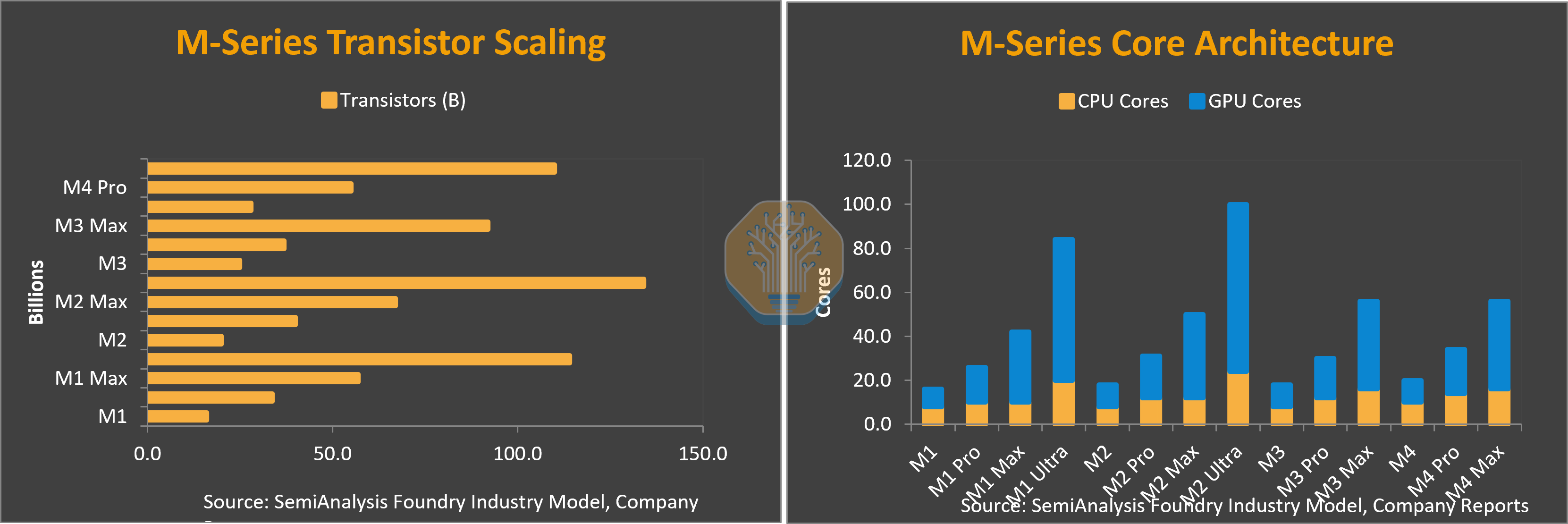
The result of this manufacturing dominance is a performance lead that has compounded over a decade. Apple’s ability to move to the next node first allows it to pack more transistors into the same thermal envelope, maintaining a performance-per-watt lead over the x86 ecosystem.
The transistor count growth is linear, but performance per watt is the real metric. The shift to N3E in the A18/M4 generation prioritized cost and yield over pure density scaling (compared to N3B), which explains the relatively modest transistor count jumps compared to previous generations. The Neural Engine has seen the most exponential growth, jumping from 0.6 TOPS in A11 to 35 TOPS in A17/A18, reflecting Apple’s strategic pivot to on-device AI years before the “AI PC” hype cycle began.
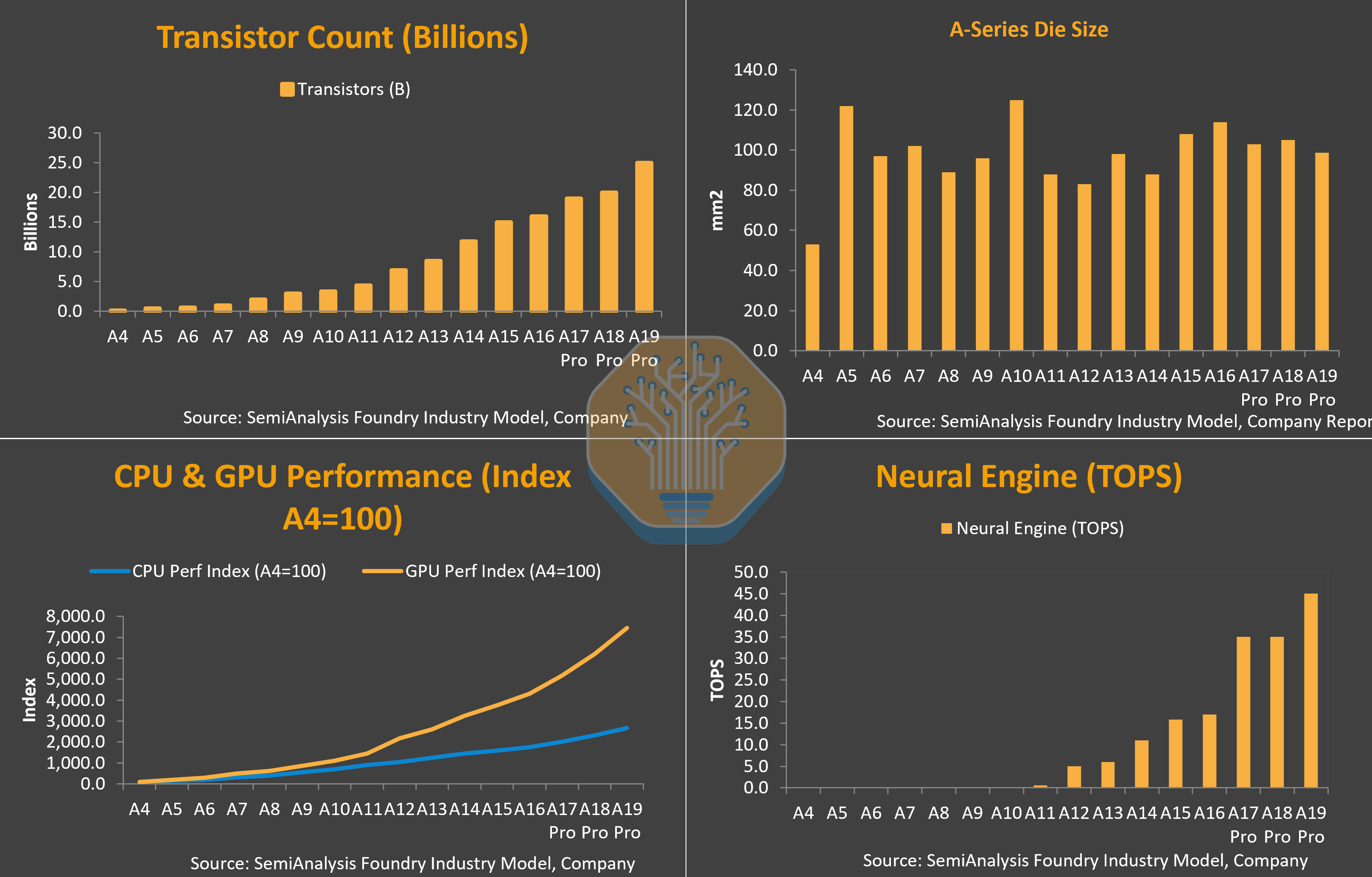
Since 2013, Apple has consistently shipped industry-first features 12-24 months ahead of competitors.
Apple Silicon Technical Advantages
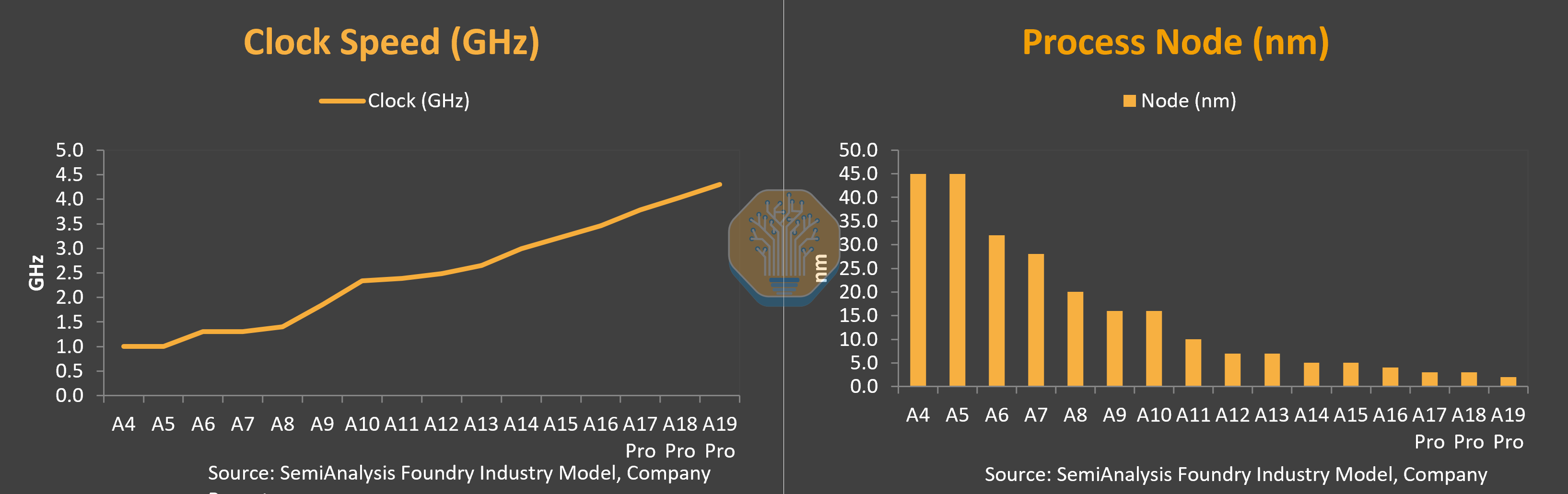
Apple’s performance leadership stems from architectural bets made a decade ago. While Intel and Qualcomm chased 5GHz+ clock speeds, Apple pursued ‘wide and slow’, executing more work per cycle at lower frequencies.
Front-End Architecture: Decode Width Parity
Apple introduced 8-wide decode with A14/M1 in 2020, four years ahead of competitors. But by 2025, the competitors caught up.
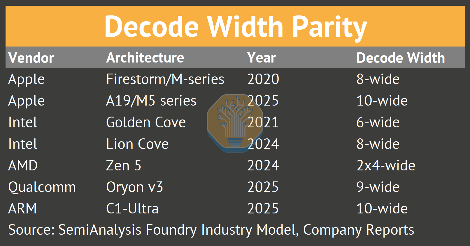
Decode width is no longer Apple’s moat. The advantage has shifted to cache hierarchy, vertical integration and extremely efficient smaller E-cores.
Cache Hierarchy: Where Apple Still Leads
Apple’s philosophy: massive fast L1, large shared L2, and a System-Level Cache (SLC) before DRAM. The SLC allows CPU, GPU, and Neural Engine to share data without hitting slow system memory.
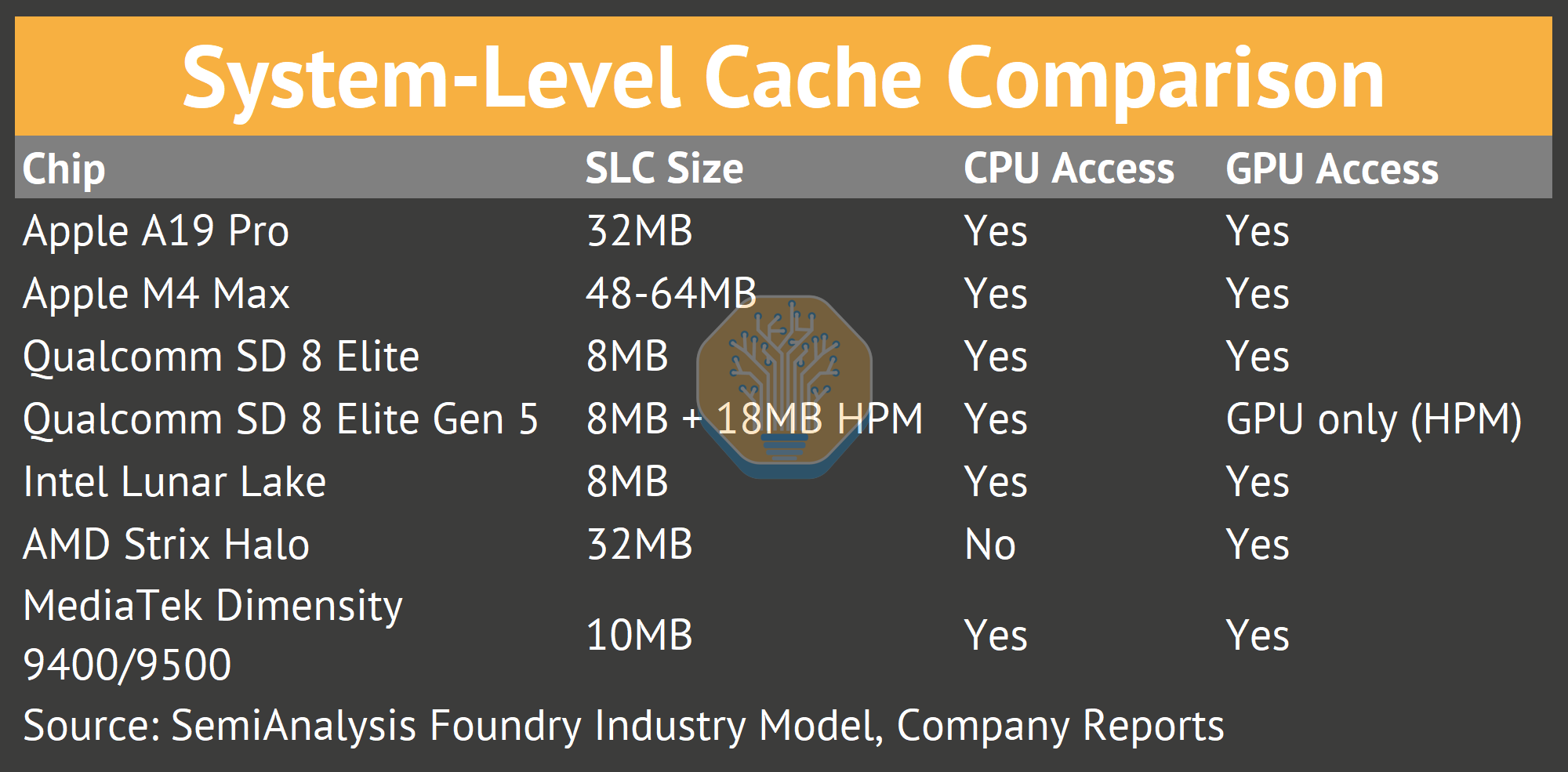
Apple’s SLC advantage is 3-4x larger than competitors with full CPU/GPU sharing. AMD’s Strix Halo matches on size but CPU cores cannot access it.
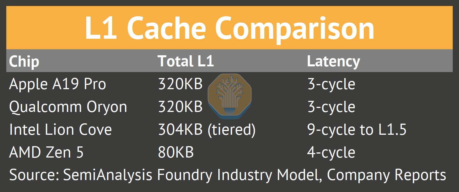
Apple and Qualcomm Oryon match on L1 size, latency and cache hierarchy, as the original Nuvia design team was largely poached from Apple. Intel’s L0/L1.5 tier structure adds latency.
Unified Memory Architecture
Traditional PC architectures have separate memory pools for CPU and GPU, requiring data copies. Apple Silicon uses Unified Memory Architecture: the GPU reads the exact same memory address as the CPU.
This eliminates the “copy penalty” critical for AI workloads. A 20GB LLM loads once. The Neural Engine and GPU access it simultaneously. Qualcomm mobile chips use shared LPDDR5X but lack Apple’s fine-grained coherency. AMD Strix Halo’s MALL is GPU-only.
Vertical Integration
Apple’s efficiency edge comes from owning the less attractive silicon: custom Power Management ICs and storage controllers enable millisecond-level dynamic voltage and frequency scaling. The chip races to sleep, completing bursts at high power and dropping to near-zero idle faster than x86 competitors.
The iPhone 17 Pro’s vapor chamber was co-designed with A19 Pro’s thermal envelope. Apple knows the exact sustained power budget (5-7W) and designs the chip accordingly. Qualcomm must design for worst-case thermal across Samsung, Xiaomi, and OnePlus implementations.
What’s changed in 2024-2025:
Decode parity: Intel, AMD, Qualcomm all reached 8-wide in 2024
SLC adoption: Qualcomm added 8MB SLC; Intel added 8MB memory-side cache
L1 parity: Qualcomm Oryon matches Apple’s 320KB L1 at similar latency
Android benchmarks closing in on iPhone’s
Xiaomi’s own XRing chips with extensive vertical integration on design, power, software
Apple’s remaining advantages: larger SLC (32MB vs 8-10MB), true unified memory with full CPU/GPU coherency, and vertical integration enabling thermal co-design. The gap has narrowed, but Apple still holds the efficiency crown.
Next we’ll dive further into specifics: Apple wafer demand and economics at TSMC, including our forecasts through the end of the decade at the A14 node. We’ll quantify Apple N2 demand and how that affects their need for older nodes - surprisingly, som older nodes are seeing increased demand from Apple. More numbers are shown for demand by chip and you’ll see the change as the company (tried to) diversify beyond the iPhone. We’ll also put numbers on the HPC phenomena as, discussed earlier, Nvidia demand encroaches Apple at the leading edge.
And there’s more: packaging economics, what TSMC’s ex-Apple business looks like, Apple’s in-house efforts to replace Broadcom modems, competing efforts to copy Apple’s vertical integration, a look at the trickle down effects in the supply chain beyond TSMC, and what the future of the TSMC + Apple partnership looks like.