

ASML has not announced anything yet, but its patent filings, a news report and its own roadmap all suggest so. We believe it will start with a die-to-wafer (D2W) hybrid bonding (HB) tool. This is harder to build than wafer-to-wafer but is where ASML could gain an edge. We see the move as a natural extension of ASML’s vertical integration, and one that should strengthen its customer ties.
In this article we unpack the tool’s design end to end, starting with patent filings. What makes it unique is that it runs on a track. That changes how the tool and the dies move: each die rides its own holder past the process stations, and the tools get closer at each station to process the dies. The track’s independent shuttles also lift station utilization, save on duplicate tooling, and enable heterogeneous integration.
We believe ASML could gain an edge in alignment accuracy and particle control for Hybrid Bonding. These are the two factors that set bonding yield. And ASML has expertise in solving the same problems in lithography.
Despite the advantages, ASML still needs to solve challenges around feed-forward metrology, the die-to-wafer contact, the modification of the non-bonding tools so they can process dies on the track, and keeping the whole loop clean.
We expect advanced logic, where D2W already runs in volume, to adopt ASML’s D2W HB tool first. This is bad news for Besi. Logic accounts for most of Besi’s HB business today concentrated at TSMC and Intel. ASML has been working with both for more than two decades and just announced a joint photomask initiative in September. We won’t be surprised to see a similar move in the back end process. Besi’s HBM prospects are also weakening. Korean challengers are catching up, in addition to an HBM adoption that we expect to slip to 2029 or beyond.
ASML is Building a Hybrid Bonder
We did a deep dive on hybrid bonding in 2024, and we still see it as the most transformative innovation in semiconductor manufacturing since EUV. Wafer-to-wafer (W2W) hybrid bonding (HB) is already in volume in image sensors and 3D NAND, and DRAM makers will be next. Die-to-wafer (D2W) HB is moving slower, because the industry still lacks mature tools that combine satisfying alignment accuracy and throughput (our check indicates upper bound in current applications is only one wafer per hour), which keeps cost per die high. Today D2W runs in volume only in logic: AMD has shipped hybrid-bonded V-Cache since 2022, and TSMC’s SoIC bonds at about 6um pitch today and targets 4.5um around 2029. The market expected HBM to become the big D2W volume driver from 2028. However, our view is different: we believe HBM will not adopt D2W HB before 2029, if at all.
Besi has led D2W and is the only supplier with tools in volume production. Everyone else is still trying to get a first tool qualified. But we believe the situation will soon change, because ASML is building a D2W hybrid bonding tool. Management hasn’t announced anything yet. But the company filed 27 bonding patent families between December 2022 and November 2024, most of them D2W, and the true count is likely higher because filings made after November 2024 are not yet public. The Elec also reported in March that ASML had started the architecture design of a hybrid bonder with Prodrive Technologies and VDL ETG.
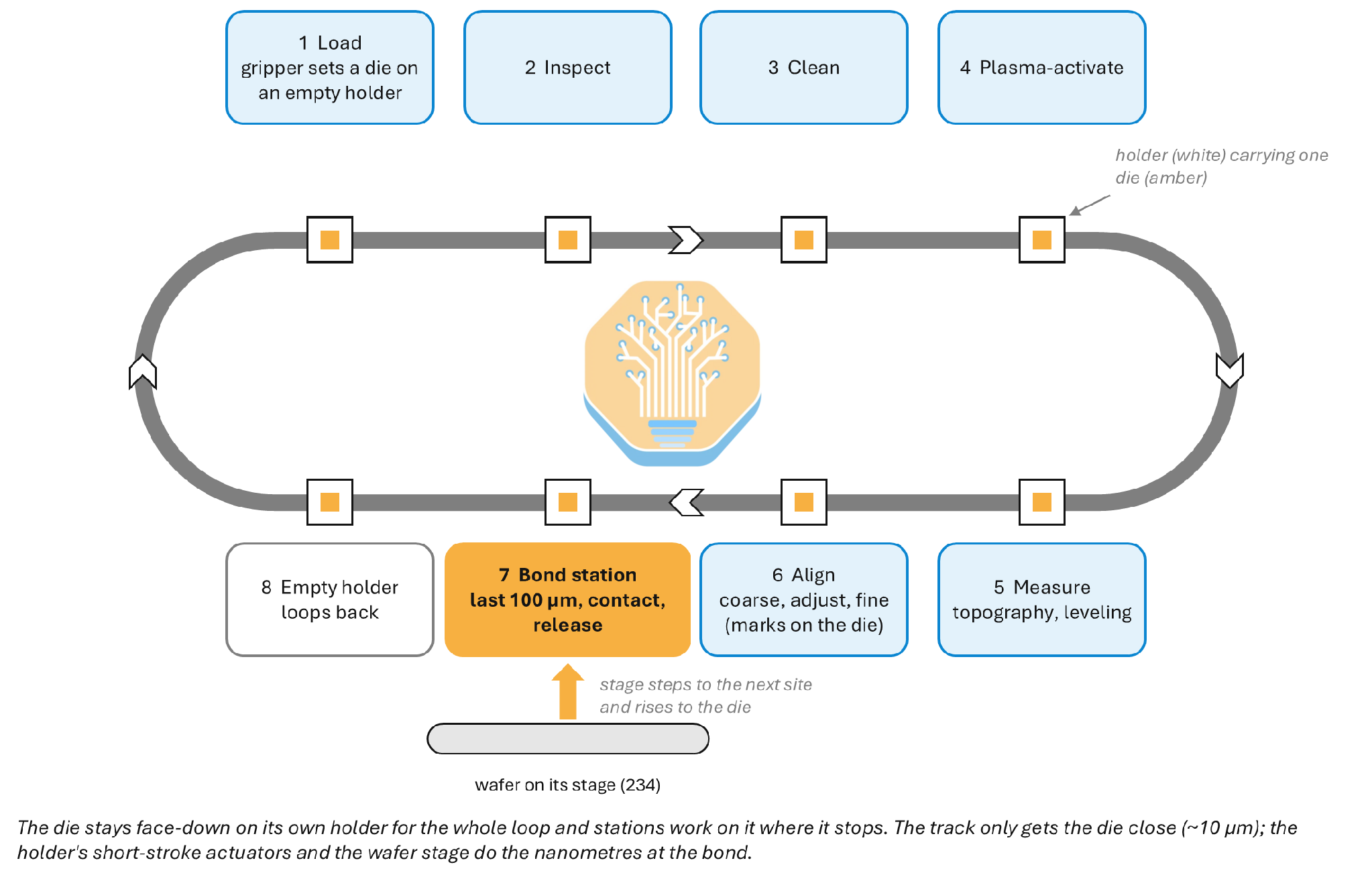
In the anchor filing (WO2025201788A1), ASML drew how its bonding flow works. Interestingly, the system looks nothing like a traditional D2W bonder (see Advanced Packaging Part 5 for how those work). Instead of a bond head picking each die off a diced wafer and placing it, ASML moves single dies on independent holders around a track (Fig 1). Each die passes inspection, cleaning, plasma activation and metrology (topography, leveling and alignment) stations before it reaches the bonding station where the chuck lifts the bottom wafer up to meet the die. We unpack the design in the sections below.
Fig 1: ASML’s track-based D2W bonder, SA annotated and simplified
ASML could be building a W2W hybrid bonding tool as well. According to a patent analysis by Inha University, ASML is likely building W2W HB equipment on its TWINSCAN platform, leaning on its wafer overlay accuracy. We focus on the D2W machine in this note, because it is the harder tool to build and the one where ASML could gain a real edge.
…as Part of its Vertical Integration Initiative
We believe this is a continuation of ASML’s effort to integrate vertically and tighten customer relationships. ASML bought Cymer for its light source in 2013, HMI for e-beam inspection in 2016 and Berliner Glas for optics modules in 2020. It shipped its first back-end product, the XT:260 i-line packaging scanner, in 3Q25. And most recently, ASML announced joint initiatives with TSMC, Intel Foundry and Samsung to move the industry from 6-inch to 12-inch photomasks for High NA EUV.
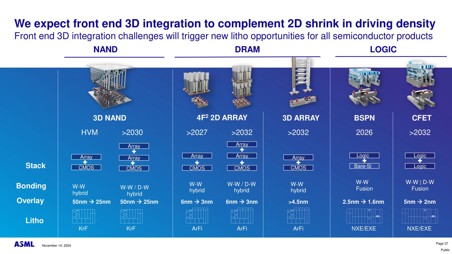
Building a bonder would be a natural next step. In fact, ASML’s own roadmap already puts bonding inside the front-end flow. Its 2024 Investor Day listed W2W and D2W hybrid bonding for NAND, DRAM and logic (Fig 2). And a July 2024 filing shows how the bonder and the scanner would work together by sharing die position data. Today a scanner printing on a bonded wafer must pre-align and coarse-align every die before it can expose. In ASML’s design the bonder already knows where it put each die and hands that map (a “coordinate system” in the filing) to the scanner, which checks a few marks and exposes. Customers get faster lithography on bonded wafers, and ASML gets to sell the bonder and the scanner as a pair.
Fig 2: ASML’s map of front-end 3D integration
We expect advanced logic to be the first adopter. Logic is where D2W HB already runs in volume, and where the alignment requirement keeps tightening. TSMC calls overlay “always the biggest challenge” for SoIC. As its HB pitch moves from 6um to 4.5um by 2029, the placement accuracy requirement will tighten further. ASML is strong in alignment, as we will elaborate below, so an edge here should help it win logic customers first. Advanced logic dies are also among the most expensive chips, so logic customers can afford a premium tool. We expect ASML to price its tools at a premium to peers.
In the next three sections, we discuss (1) the tool’s track system - the most unusual thing about it compared with what is on the market; (2) how ASML’s strengths in alignment, particle control and motion could make its HB tool superior; and (3) the challenges ASML or its supply chain partners still need to resolve to build a working tool. Let’s dive in.
What’s Unique About the Tool
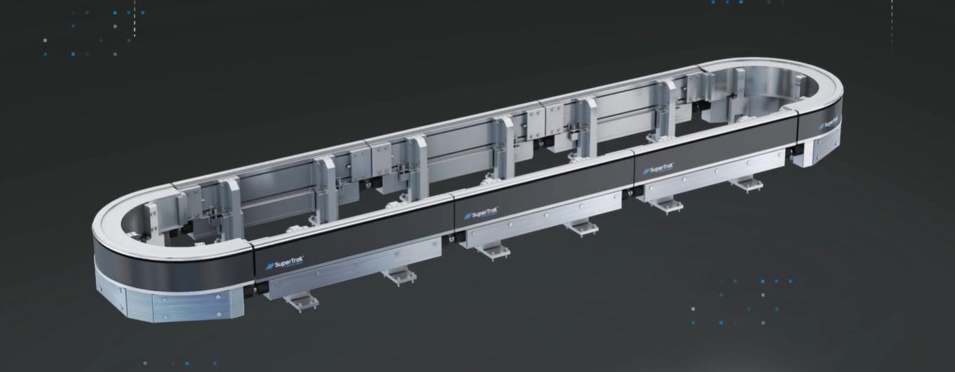
One of the most interesting things about the tool is that it runs on a track. ASML names SuperTrak CONVEYANCE (Fig 3) as an example in its patent filing, so we assume it uses that track and we base our analysis on the track’s published design.
The fundamental difference from a traditional bonder is where the die lives. In a Besi-type tool, the die is prepared elsewhere, and a bond head picks it up only for the final placement. In ASML’s design, each die sits on its own holder from the moment it leaves the carrier and stays there until the bonding step. The process stations are built around the track: the die stops in front of a station, the station cleans, activates or measures it in place, and the die moves on.
Fig 3: SuperTrak CONVEYANCE track (HORIZON10 platform)
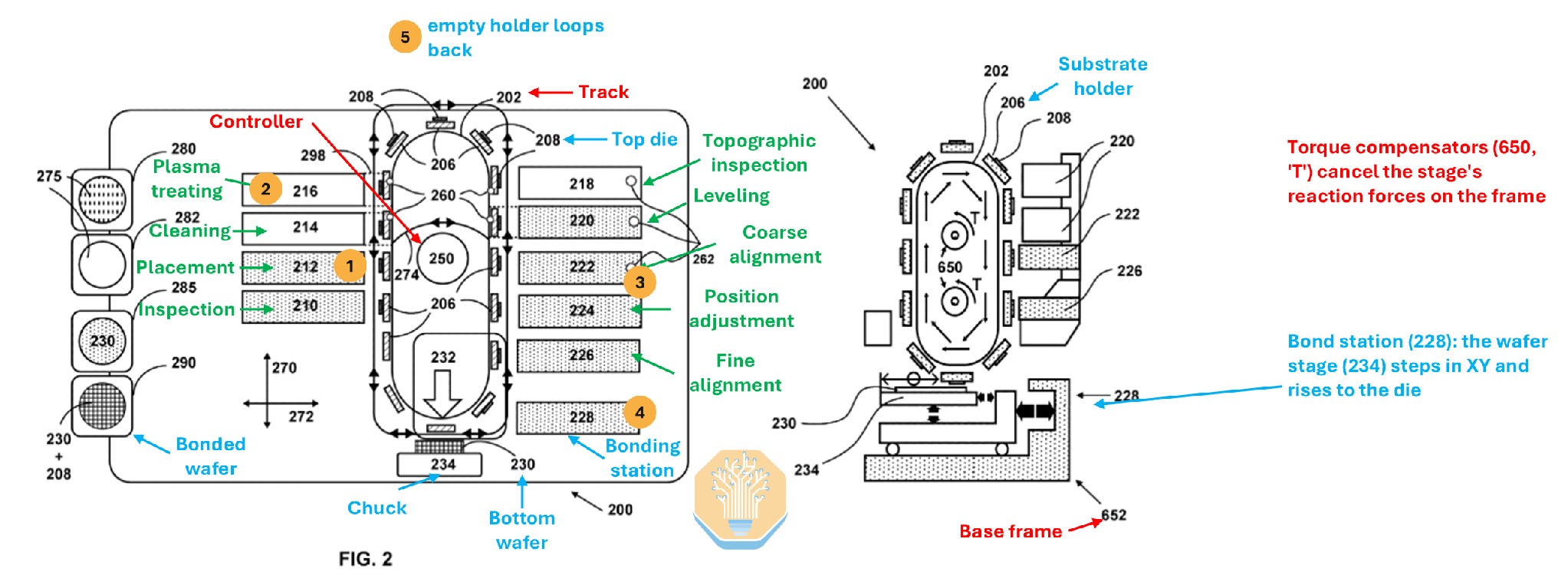
Now let’s go through the process step by step. For illustration, we took the patent drawing and labelled every station in Fig 4. A gripper takes the die off its carrier and sets it on an empty substrate holder (206), which carries it along the track (202). The die stops in turn at the inspection, cleaning, plasma activation, topographic inspection, leveling, coarse alignment, position adjustment and fine alignment stations (210 to 226). At each stop the die stays on its holder, and the station does its work. Note the reversal here: in the patent it is the station’s sensor or head that moves in to reach the die, not the die that is carried into the tool as in today’s flow. After these steps the die arrives at the bonding station (228).
This bonding station deserves a closer look. The first thing to note is that the final placement is done by the holder (206) and the chuck (234), not the track: SuperTrak’s spec sheet puts the shuttles’ repeatability at about 10um, nowhere near the 50nm placement accuracy the bond needs. Next, zoom in on the right-hand part of Fig 4 for the bonding work. The chuck lifts the bottom wafer to within tens of microns of the die, the holder’s actuators adjust the die’s position, the die is pressed onto the wafer to form the bond, and the holder releases it. The empty holder then starts another loop.
Fig 4: Patent WO2025201788A1 Fig. 2 (left) and Fig. 6 side view (right), SA annotated
This design has three major benefits:
First, independent shuttles lift the utilization of every station. The number of stations per step can be set from that step’s cycle time: a three-second cleaning step gets three stations, and a 1.2-second bond step gets one, so every station stays busy. The patent asks for exactly this, to “occupy all process stations simultaneously”.
Second, capacity is added by adding a station rather than a second tool, as long as the equipment chamber has room for it. That saves duplicate tooling and budget.
Last but not least, the design suits heterogeneous integration: a new die type is a new software recipe, so mixed chiplets could share one line.
That said, the track brings its own challenges around the non-bonding stations and the cleanliness of the whole loop. We come back to them later.
How ASML May Gain an Edge
Before that, let’s look at how ASML could bring its existing strengths to the HB tool.
First, a reminder of why alignment accuracy and cleanliness matter so much in hybrid bonding. As we elaborated before, a single 1um particle between two full-thickness wafers can unbond an area around 10mm across, resulting in a defective bond (Fig 5). So particle control is extremely important for HB. Alignment matters for two reasons: placement accuracy sets bond yield directly, and alignment time weighs far more on D2W throughput than on W2W because it compounds with the die count. These two hurdles are what make hybrid bonding almost a front-end process.
Fig 5: A small particle opens a void and an open contact in hybrid bonding

We believe ASML can tackle both with decades of experience solving the same two problems in lithography.
For alignment, we believe ASML can reuse its wafer-alignment sensor technology. Based on its patent filings, the bonding system puts a tiny diffraction grating on each die and reads the die’s position from the light the grating scatters. The principle is the same as ORION, the wafer-alignment sensor on every new TWINSCAN since 2017. ORION was built to read marks that CMP and etch have tilted or deformed (Fig 6), and a mark on a bonding die goes through the same CMP and plasma activation as the copper pads next to it, so it carries the same asymmetry. We believe the same sensor family can serve the D2W bonder.
Fig 6: A symmetric and a tilted alignment mark. Process steps shift the apparent center; ORION’s multi-color readout was built to see through that

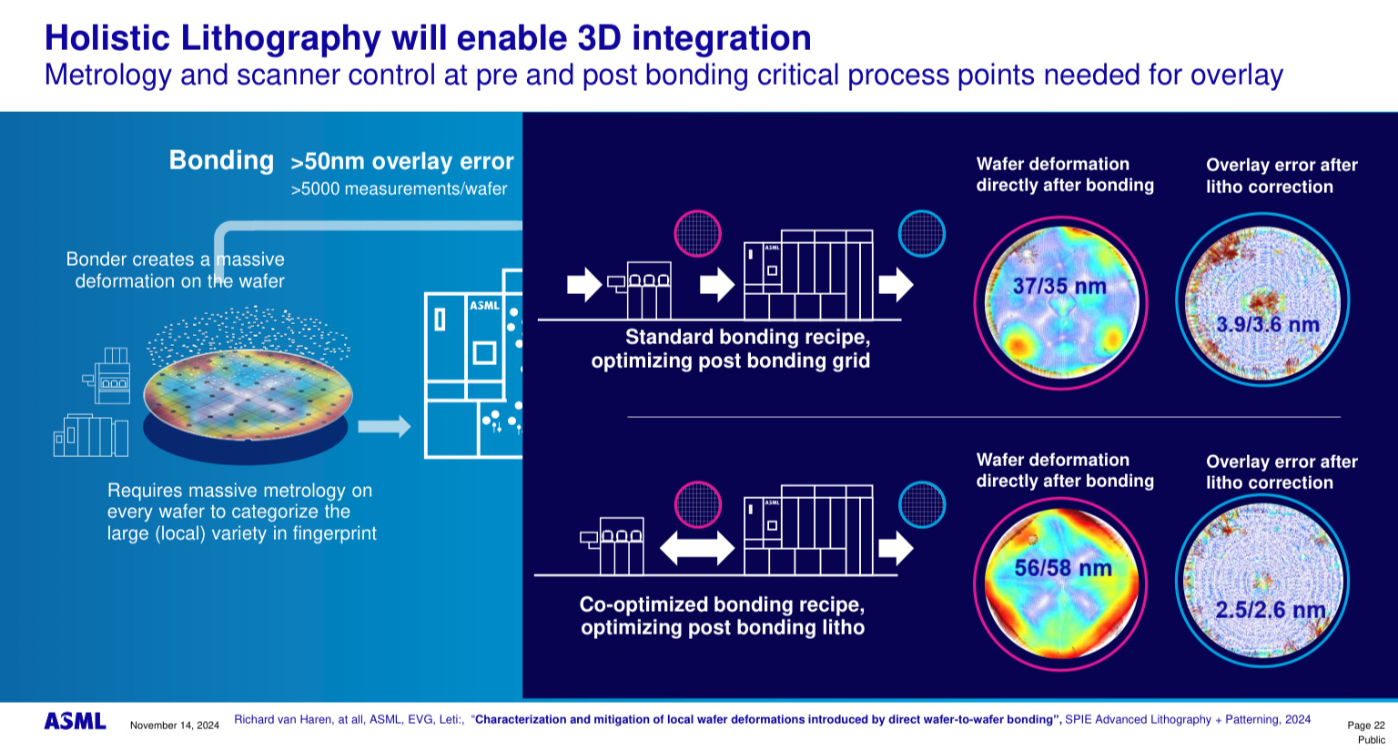
Its sensing and motion capabilities also provide it with more room in total alignment error budget. Its NXT:2100i holds 0.9nm overlay on a single machine. And ASML can already measure the distortion of a W2W bonded wafer and correct the next lithography layer for it, bringing post-bond overlay from 40-60nm down to below 4nm (Fig 7). These are litho numbers, not bond results. But they mean ASML’s sensor and stage errors sit more than an order of magnitude below the 50nm a bonder needs. Higher stage precision leaves more room in a bonder’s error budget for the other factors: die shift on the holder, thermal drift and movement during contact.
Fig 7: ASML metrology plus scanner correction brings post-bond overlay to 2.5-3.9nm
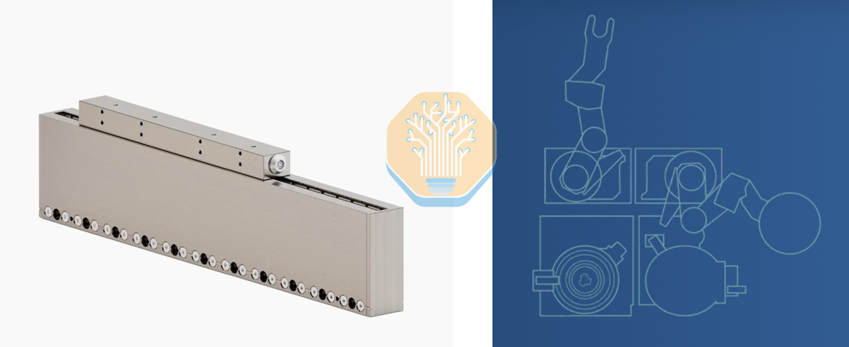
Prodrive Technologies and VDL ETG are the likely component suppliers to help ASML’s bonder move fast on motion. Prodrive makes the linear motors and drives for ASML’s EUV maglev stages and has also built Hanwha Semitech’s SHB2 Nano bonder. VDL ETG builds ASML’s frames and modules (Fig 8).
Fig 8: Prodrive’s linear motor (left) and VDL ETG’s wafer handler module (right)
On cleanliness, the requirements for ASML’s EUV systems are more strict as a bonder’s. Few tool makers have fought particles at the nanometer scale for as long as ASML. EUV scanners move reticles and wafers in vacuum and keep reticle particle adders at a level “compatible with HVM requirements for sub-10nm node lithography”. We believe ASML has thought about the bonding surfaces too: its bonding apparatus filing adds a tool that cleans the substrate supports and a sensor that watches their flatness, particle load and distortion.
That said, contaminants in a bonder differ from those in a scanner. Most are dicing debris on die edges and particles landing on freshly activated, hydrophilic surfaces. We look for more detail on how ASML handles these bonder-specific contaminants in future filings.
After the paywall we discuss the challenges ASML needs to tackle to build a working tool, and how its tool will impact on Besi’s business prospects.