

Die Size And Reticle Conundrum – Cost Model With Lithography Scanner Throughput
Smaller Chiplets Isn't Always Better
We have been spending a lot of time in our private consulting business trying to build out a model of semiconductor fab capital expenditures by tool type for various logic and memory process nodes. The item we are tracking very closely is how lithography spending is evolving across various node shrinks. Our starting point has been 28nm and it evolves through the first generation of FinFET nodes to the first EUV nodes through to the first Gate All Around Nanosheet nodes (3nm and 2nm). The percentage spent on lithography differs quite a bit depending on what node is examined. For posterity’s sake, here is an old ASML slide on the topic. It seems to exclude a lot of various fab capex spending, but interesting to look at.

The evolution of lithography spending versus deposition versus etch has a lot of impact on the relative performance of companies such as ASML, Lam Research, Applied Materials, Tokyo Electron, etc. As we worked through this, the single most important aspect has been cost per exposure per DUV or EUV layer, and the number of them. By the way, some sell-side analysts have attempted to work in number of EUV exposures per node into their ASML models, and it’s all hilariously wrong.
At this point you’re probably thinking, gee Dylan, that’s great, but what does that have to do with die sizes?
The conventional wisdom is that bigger dies cost exponentially more. We think that all of our readers know this. Larger die sizes increase costs because defects are more likely to affect that larger die. This is one of the major driving forces behind the chiplet revolution. We put numbers to that in our advanced packaging series using AMD chiplet datacenter CPUs vs Intel monolithic datacenter CPUs.
This conventional thought process can be completely wrong. Let’s use a hypothetical example with pictures to explain how a smaller die could be more costly to manufacture. Let’s say a fabless chip design team is deciding between making a single large monolithic die or 2 chiplet MCM design. On the left is a wafer full of dies that are 25mm by 32mm, 800mm2. On the right is a wafer full of dies that are 13.5mm by 32mm, 432mm2. The 2 chiplet design would only be 8% more silicon per chiplet which is similar overhead to what AMD experiences with their current chiplet CPUs. The number of dies without defects differs between the two designs hugely despite both nodes having been simulated to have the same number of defects per cm2 (0.1).
The monolithic design has 30 good dies per wafer where as the chiplet MCM design has 79 good dies per wafer. Let’s assume all defective dies must be tossed in the trash. If there is no die yield harvesting, the design company can only sell 30 products per wafer with the monolithic design, but the chiplet MCM design can sell 39.5.

That’s ~30% more products per wafer by going to chiplets and MCM. If the assumption is that each wafer costs $17,000, then monolithic costs $567 for the defect free silicon die and the chiplet MCM will cost $215 per defect free silicon die and $430 for the 2. Clearly the design team should choose the chiplet MCM option if we ignore any power consumption, die harvesting, and packaging costs differences because they can save $136 per product!
What if we told you this chiplet MCM design is more expensive?
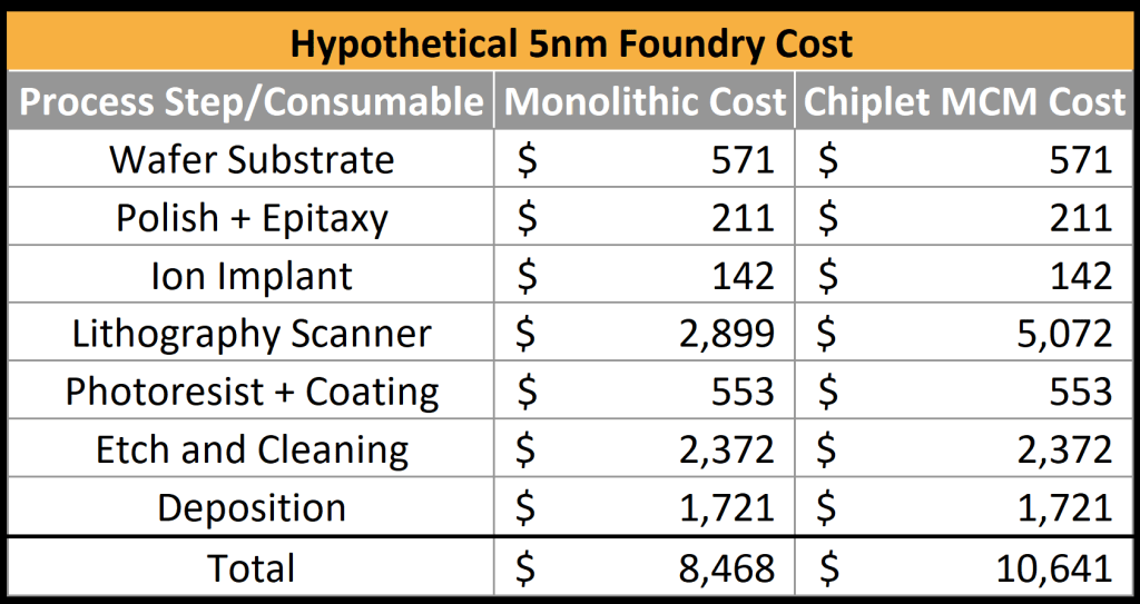
You probably wouldn’t believe us, but let’s walk through how. In this hypothetical scenario, let’s say that the products are using a foundry 5nm class node. Let’s assume this foundry sells these wafers for ~$17,000 with a ~50% gross margin. Below is a cost break down by consumable or process step including tool depreciation, maintenance costs, power usages, employee costs allocated down, etc.

These numbers are fudged heavily from our actual estimates, but the consistent thing is that the biggest cost center is lithography. It makes nearly 1/3 of the cost of the processed wafer. That lithography cost is just an average assumption. It can differ widely based on what die size you choose.
A lithography tool exposes a wafer indiscriminately. It needs to know where to expose with lithography and where not to expose. The photomask is what contains a chip design and blocks the light or allows it to go through to expose the wafer. A leading edge 5nm foundry design will have a dozen or so EUV photo masks and another few dozen DUV photo masks. Each of these photomasks corresponds to a feature or a portion of a feature on the wafer and is unique to each chip design. By cycling through lithography and all other process steps, this foundry can build out specific 5nm chips on wafers over the course of about 10 weeks. Below is a picture of a DUV photomask.
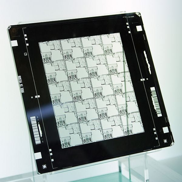
The standard photomask is 104mm by 132mm. The lithography tool then exposes through the photomask to print features on the wafer at 4x reduction. That field is 26mm by 33mm. Most designs do not line up perfectly with 26mm by 33mm.
In comes the concept of reticle utilization rates.
Generally, chip designs are smaller, so the photomask can contain multiple identical designs as with the picture above. Even then, most designs will not fit perfectly onto that 26mm by 33m field, so generally a portion of that photomask is also not exposed.
If a die was 12mm by 16mm we could fit 4 dies per reticle. The reticle utilization rate is quite high here as only a tiny sliver of the reticle is not exposed. With a monolithic die which is 25mm by 32mm, we do not utilize 1mm on the slit and scan directions. That reticle utilization rate is likewise, quite high. In the case of our chiplets which are 13.5mm by 32mm. This die is too large to fit 2 side by side on the reticle, so there can only be 1 die per reticle. Some visualizations of the examples described above are shown in the graphic below.

You may ask, what is wrong with low reticle utilization rate?
It becomes a huge cost problem because of what happens when we zoom out to the process of processing on a wafer level. A wafer placed in a lithography tool and tool exposes a portion of the wafer 1 reticle field at a time. If the full 26mm by 33mm reticle is utilized, the lithography tool steps over the 300mm wafer in the minimum number of steps, 12 reticle fields wide and 10 reticle fields tall. If reticle utilization rate is lower, then the tool must step over and across the wafer more times in each direction.
When comparing our 25mm by 32mm monolithic die on each wafer versus the 13.5mm by 32mm chiplet MCM design, we need to step over the wafer 1.875x as many times!
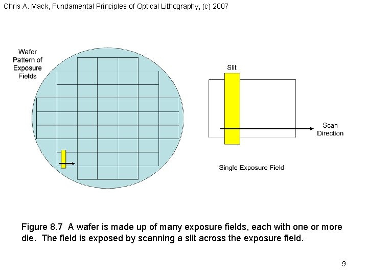
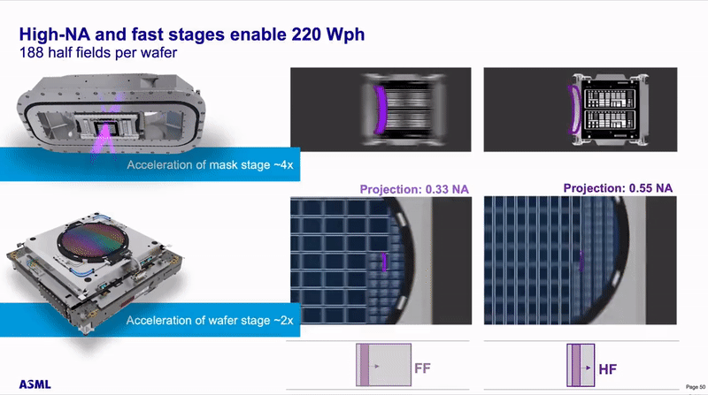
Modern DUV and EUV tools have a slit and a scan. The slit (26mm) is what is exposed, and it scans (33mm) across the reticle area. This gif below that Andreas Schilling shared is from ASML about High-NA EUV showcases the concept. With High-NA EUV, the slit is still a 26mm maximum, and the scan is halved. The main loss of productivity is with how fast the wafer stage must move.
Imagine if instead, the slit was halved. The throughput impact would be much larger.
When comparing our monolithic design versus the chiplet MCM design, our lithography tool time is up significantly because the wafer must be scanned 1.875x as much. This is because a huge portion of the slit is underutilized. While there are still some efficiencies in terms of wafer loading times, the bulk of the cost of a lithography tool is with scan time. As such the internal cost per wafer is up significantly.
In this hypothetical scenario, the foundry is now spending $2,174 more per wafer in lithography cost. This is a huge cost increase that a foundry does not stomach for their large volume customers who already have very tight margin deals. Let’s say the foundry is pricing to margin and as such maintains their 50% gross margin regardless of the design.
The cost increase on underutilizing the slit on the reticle means that the foundry would not sell these wafers for $17,000 to sustain 50.2% gross margins. Instead, they would be selling these wafers for $21,364. The defect free silicon cost for the monolithic product still sits at $567. The defect free silicon cost per die isn’t $215, but instead $270. Per product, it is no longer $430, but instead $541.
The decision of chiplet vs monolithic becomes a lot more difficult now. Once you account for packaging costs, it is very likely the monolithic die is cheaper to fabricate. Furthermore, there are some power costs with the chiplet design. In this case, it is absolutely better to build a large monolithic die instead of going chiplet/MCM.
This example is a worst-case scenario chosen to demonstrate the point of reticle utilization rates. There are also a ton of caveats with this simplistic and hypothetical analysis. Furthermore, most other process nodes before 5nm as well as after we move into the gate all around era, have lower lithography costs relative to other process steps. Most chiplet architectures are likely going to increase reticle utilization rates rather than decrease it.
This is a rabbit hole we went down for a couple days that ended up having no impact on our work or task, but we wanted to share what we learned. Special thanks to Cyrus Tabery for helping us think through the publicly available concepts related to reticle utilization rates that we presented.
The chiplet would be laid out in a more sensible proportion, using the full 26mm width of the reticle as much as possible, and dividing the height by half, plus the overhead for interconnect. So the tool throughput will drop more like 10% (counting extra stepping movements and extra area), not 87%.
"here is an old ASML slide the topic"
"here is an old ASML slide ON the topic"
"The evolution lithography spending versus deposition versus "
"The evolution OF lithography spending versus deposition versus "
"Let’s assume this foundry WHICH sells these wafers for ~$17,000 with a ~50% gr"
"Let’s assume this foundry sells these wafers for ~$17,000 with a ~50% gr"
Not sure about the last one. Great content as always