

Dissecting Nvidia Blackwell - Tensor Cores, PTX Instructions, SASS, Floorsweep, Yield
Microbenchmarking, tcgen05, 2SM MMA, UMMA, TMA, LDGSTS, UBLKCP, Speed of Light, Distributed Shared Memory, GPC Floorsweeps, SM Yield
Nvidia’s Datacenter Blackwell GPU (SM100) represents one of the largest GPU microarchitecture change in a generation, yet no detailed whitepaper exists. Until today, there is no public datacenter Blackwell architecture microbenchmarking study on PTX and SASS instructions, such as UMMA and TMA, with a focus on AI workloads.
After our in-depth Nvidia Tensor Core Evolution: From Volta To Blackwell article, SemiAnalysis has spent months of engineering time, tearing into the Blackwell architecture and measuring the raw PTX instruction performance, to establish hard practical performance upper bounds and compare them with the theoretical peaks. We do this to discover unit- and instruction-level hardware throughput and latency limits, providing a useful characterization from an ML systems and kernel development perspective. We focus on deep learning workload configurations, such as benchmarking asynchronous memory copy setups used in popular deep learning library FlashInfer.
We open sourced our Blackwell micro-architecture-level benchmarking repo here. Please drop a star if you find it useful.
Acknowledgement
We thank Nebius and Verda for providing B200 nodes for microbenchmarking. Their B200 nodes have the correct hardware counters enabled that makes NCU profiling possible. For users on cloud providers that don’t have NCU enabled, here is a workaround suggested by GPU Mode Mark Saroufim. We would also like to thank the authors of Dissecting the NVIDIA Hopper Architecture through Microbenchmarking and Multiple Level Analysis and tcgen05 for dummies, whose work we based our code upon.
Finally, we’d like to thank all our reviewers and external collaborators:
Kilian Haefeli - Cohere
Benjamin Spector - Flappy Airplanes and Stanford
Neil Movva - Sail Research
Orian Leitersdorf - Decart AI
Hardik Bishnoi - Arcee AI
And many anonymous reviewers


Future Work
This article is the first in a series exploring low-level assembly and kernel code of AI accelerators. In future installments, we will expand the effort by benchmarking additional Blackwell and Blackwell Ultra PTX instructions, including EXP2 and TensorMap update latencies. Furthermore, we have concrete plans to benchmark TPU Pallas kernels, Trainium NKI kernels, and AMD CDNA4 assemblies. For AMD CDNA4 in particular, benchmarking is within reach in the near term since many of the instructions are already well-documented.
Join us if you want to work on low level benchmarking, ClusterMAX, inference simulators, or other interesting technical work. Send your resume to letsgo@semianalysis.com with 5 bullet points demonstrating your exceptional engineering abilities. Please attach GitHub repo links, YouTube demos, websites, blogs, etc to support your bullet points.
Blackwell Features
From Hopper to Blackwell, NVIDIA made several incremental improvements to the architecture and changes to the PTX abstractions for MMA-related instructions. We cover most of these in our article NVIDIA Tensor Core Evolution. The major notable changes are:
The introduction of tensor memory (TMEM) to hold MMA accumulators. Threads no longer implicitly own the results of MMA operations and instead, TMEM is explicitly managed at the MMA scope from software
tcgen05operations are now issued by a single thread on behalf of the entire CTA, rather than at warp or warpgroup scope as in previous generations. You can see this reflected in the CuTe MMA atoms which now useThrID = Layout<_1>in Blackwell instead ofThrID = Layout<_128>as in the warpgroup-scoped MMAs of HopperSupport for TPC-scoped TMA and MMA across pairs of coordinating CTAs, exposed as
cta_group::2in PTX and2CTAin SASS, where two SMs making up a TPC can executetcgen05.mmaon shared operands, providing access to higher operational intensity MMA instructions by reducing per-CTA SMEM bandwidth requirements. Later we show that this operand sharing is necessary to make use of the available MMA throughputNative support for sub-byte datatypes with micro-scaling
Cluster Launch Control (CLC) as hardware support for dynamic work scheduling in persistent-CTA kernels (Covering in future articles)
Programmatic dependent launch (PDL) was introduced in Hopper to hide launch and setup latency in back-to-back kernels (Covering in future articles)
Clusters, GPCs, and Floorsweeping
Since Hopper, Nvidia datacenter GPUs have supported an optional feature which is known by several names, such as “thread block clusters”, “CTA clusters”, and “cooperative grid arrays” (CGAs), all of which refer to the same feature. A cluster is a logical grouping of CTAs, the shape and size of which can be statically or dynamically specified per-kernel. Clusters are visible to the programming model in some useful ways, one of which allows for multicast loads to multiple CTAs in the same cluster; we discuss this later in the context of TMA multicast.
Importantly, CTAs in a cluster are guaranteed to be co-scheduled on the same GPC. This has an important consequence in the 1-CTA-per-SM “persistent CTA”-style Blackwell kernel: if the cluster size does not evenly divide the number of SMs in a GPC, some of the SMs will be left idle. This behavior can be confusing for kernel authors who, unaware of the sparsely-documented GPC, naively launch a number of persistent CTAs equal to the number of SMs with clusters enabled, resulting in serialized execution for some CTAs.
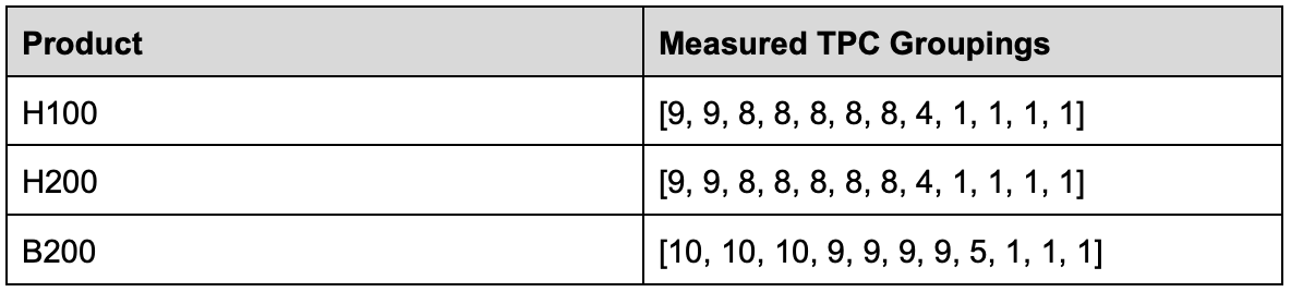
The number of yielded SMs per GPCs is not fixed, not the same between GPCs on the same chip, and may not even be symmetrical between dies in the same package. Manufacturing of semiconductors results in defects and those defects can land all over the chip. As such Nvidia has to engineer their chips in a way such that they can still have those yielded units still exposed to software in a relatively uniform way.
We prompted Claude to write a utility to reverse-engineer the mapping of SMs to GPCs by launching clusters of various sizes and using PTX %%smid to record which SMs appear in the same GPC. The result is a list of logical groupings of TPCs into GPCs. The list is longer than the 8 GPCs present in Hopper/Blackwell because there are some TPCs which seem to occupy their own logical GPC, and are never co-scheduled with any other TPCs.
As of SM100, NVIDIA has provided a solution to this quantization issue so that kernels can get the benefit of larger clusters while still making use of all the available SMs. Kernels can be launched with two cluster sizes: a preferred cluster size and a fallback cluster size. In general, to use the whole GPU, the fallback cluster should be size 2 or size 1.
References:
CU_LAUNCH_ATTRIBUTE_PREFERRED_CLUSTER_DIMENSION
Logical vs. Physical GPC
The groupings of TPCs into GPCs we presented above are logical groupings. They represent software’s view of the GPCs, with no information about which of the 20 actual physical SMs in each GPC are enabled, or where each physical GPC is located on the two dies. In reality, B200 chips with the same logical configuration need not have exactly the same physical SMs yielded in each GPC. This can be a potential source of performance non-determinism between GPUs which otherwise might look the same from the view of software. Additionally, the logical groupings of SMs into GPCs tells us nothing about which GPC is on each of the two dies in the B200 package.
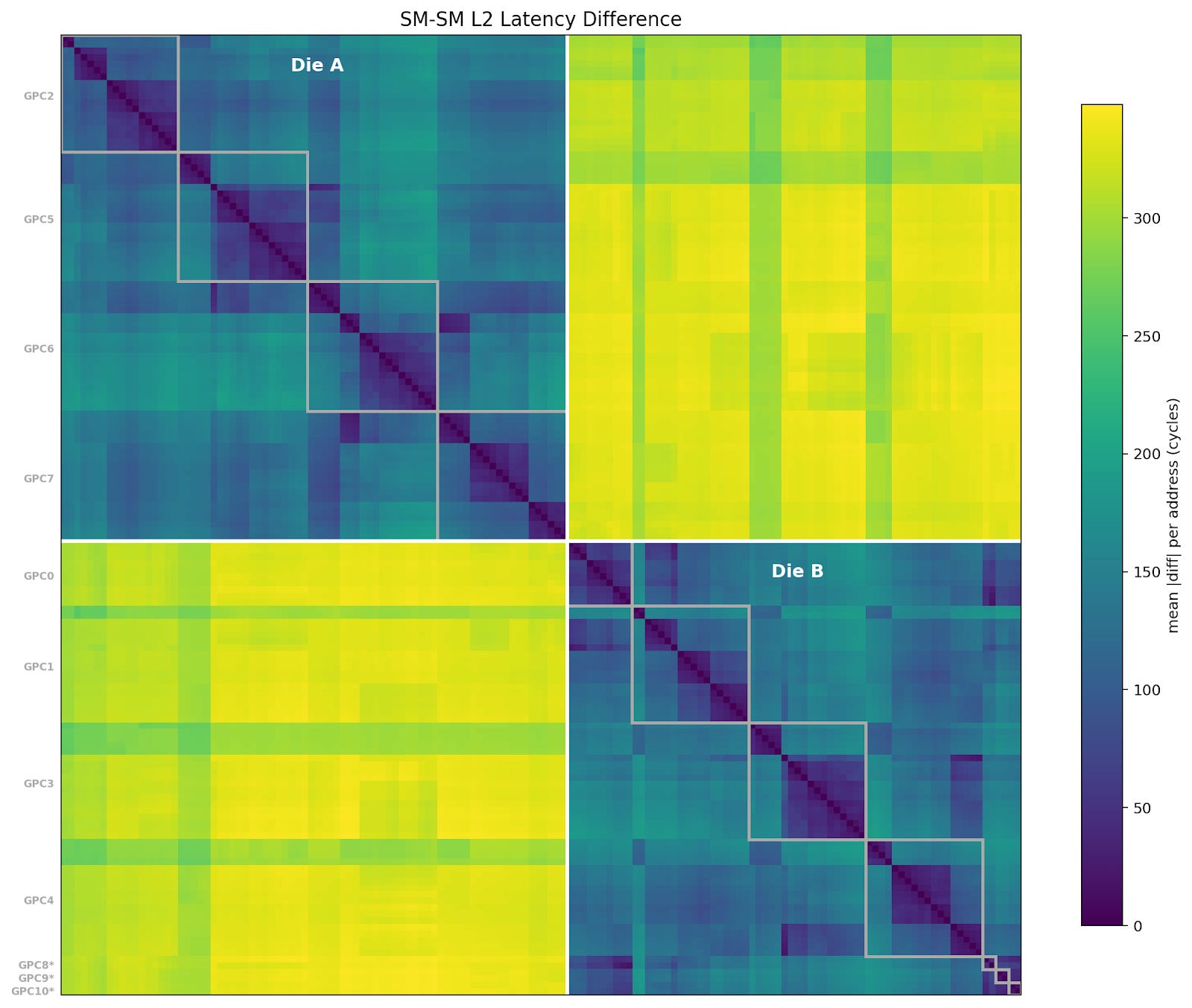
To discover more information about the physical layout of the SMs, we have every SM traverse a pointer-chase array that fills L2 cache, measuring the latency of each load. For each address, we compare the latency seen from each SM to the latency seen by every other SM, to produce an SM<->SM distance matrix. X and Y axes are SM ID.
We can see two clear sets of SMs, separated by >300 cycles average distance to L2; this must be the die-to-die crossing. We’ve also labeled the SMs with their logical GPC groupings as identified in the last section; interestingly, the singleton TPCs are close together and seem to correlate well with GPC0 in this benchmark, so one might guess that those TPCs physically reside on GPC0.
Based on this information, we can refine the list of yielded TPCs for each GPC, though the 5+3 is still just a guess.
Die A: [10, 10, 10, 9]
Die B: [9, 9, 9, 5+3]
Additionally, though in a roundabout way, we can conclude that the die-to-die latency penalty is roughly 300 cycles. This is also evident when looking at the latency profile for a singular SM from the benchmark (which also includes a lot of L2 congestion):
We would like to thank Orian from Decart AI for the benchmark inspiration.
Memory Subsystem
In this section, we discuss the memory subsystem: the hardware units that move data between computation units. Memory copy instructions are operations that use the memory subsystem, and newer generations feature asynchronous copy instructions (Read the previous article for the asynchrony evolution). Here we focus on the two variants of asynchronous copy instructions: LDGSTS and TMA (Tensor Memory Accelerator).
Asynchronous Copy
Async copy (PTX: cp.async , SASS: LDGSTS) was introduced in the Ampere generation, and the instruction moves data from global memory to shared memory asynchronously. Async copy is non-blocking, allowing memory loads to overlap with computation. It also writes directly to shared memory without going through registers, reducing register pressure.
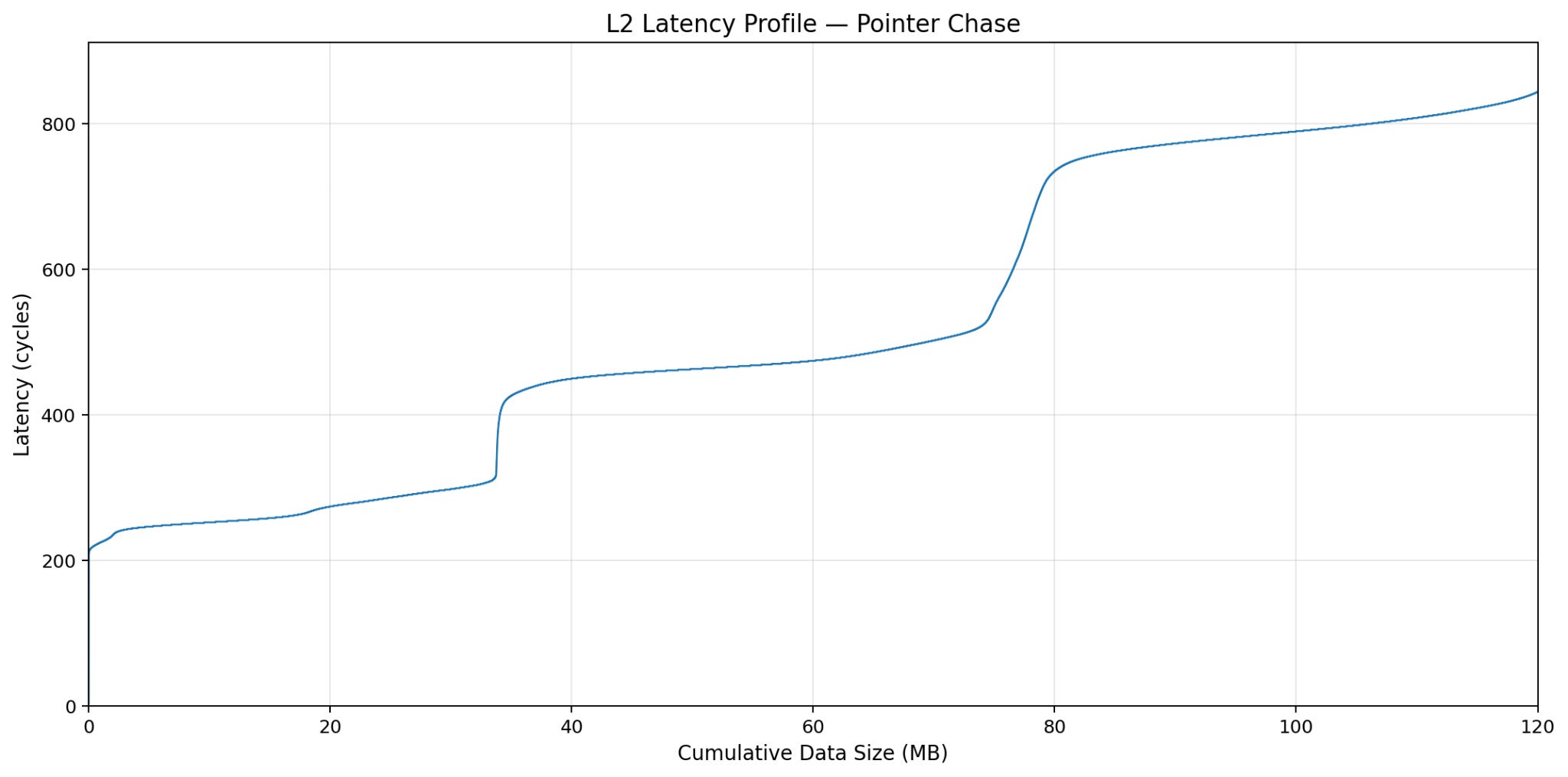
Referencing FlashInfer Multi-head attention (MHA) kernels, we benchmark async copy with the following configuration:
CTAs per SM: 1, 2, 3, 4
Number of Stages: 1, 2, 4
Threads per CTA: 64, 128, 256
Load Size: 4B, 8B, 16B
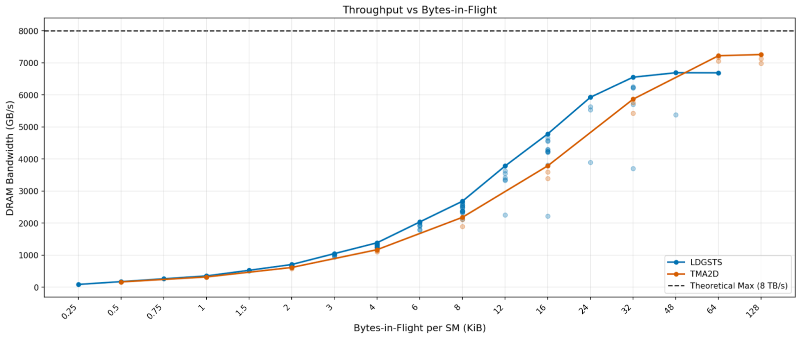
We plot throughput versus bytes-in-flight per SM, the total number of bytes concurrent memory loading instructions are loading.
Although different load sizes converge to similar throughput at the same bytes-in-flight, we prefer 16-byte loads. 16-byte loads achieve slightly higher throughput at similar bytes-in-flight while using less execution resources. For example, at 32 KiB in flight, 8B load uses 4 stages, while 16B load uses 2 stages. This saves the memory space for 2 memory barrier objects and reduces instruction issue pressure.
Overall, we see memory throughput with LDGSTS saturating at around 6.6 TB/s at 32 KiB in flight.
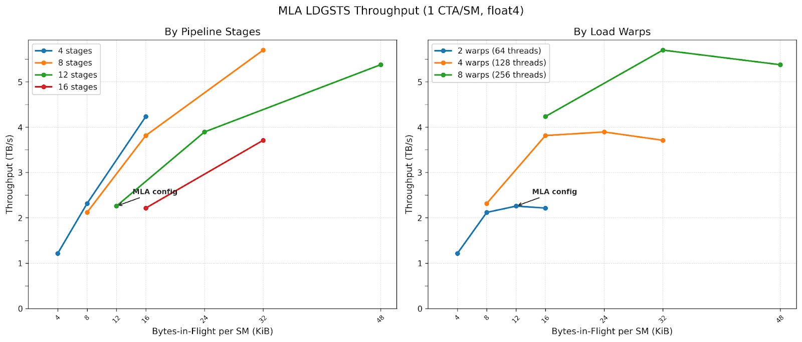
We also benchmark config space multi-latent attention (MLA) kernels use:
1 CTA per SM
16B loads
Threads per CTA: 64, 128, 256
Number of Stages: 4, 8, 12, 16
Our experiments show that increasing the number of stages achieves higher throughput at higher bytes-in-flight, and that increasing threads per CTA strictly improves performance across all configurations. Interestingly, MLA uses 2 warps and 12 stages, landing at about 2.2 TB/s . We believe this is due to softmax warps needing the most registers, and increasing warp count reduces register allocation per thread.
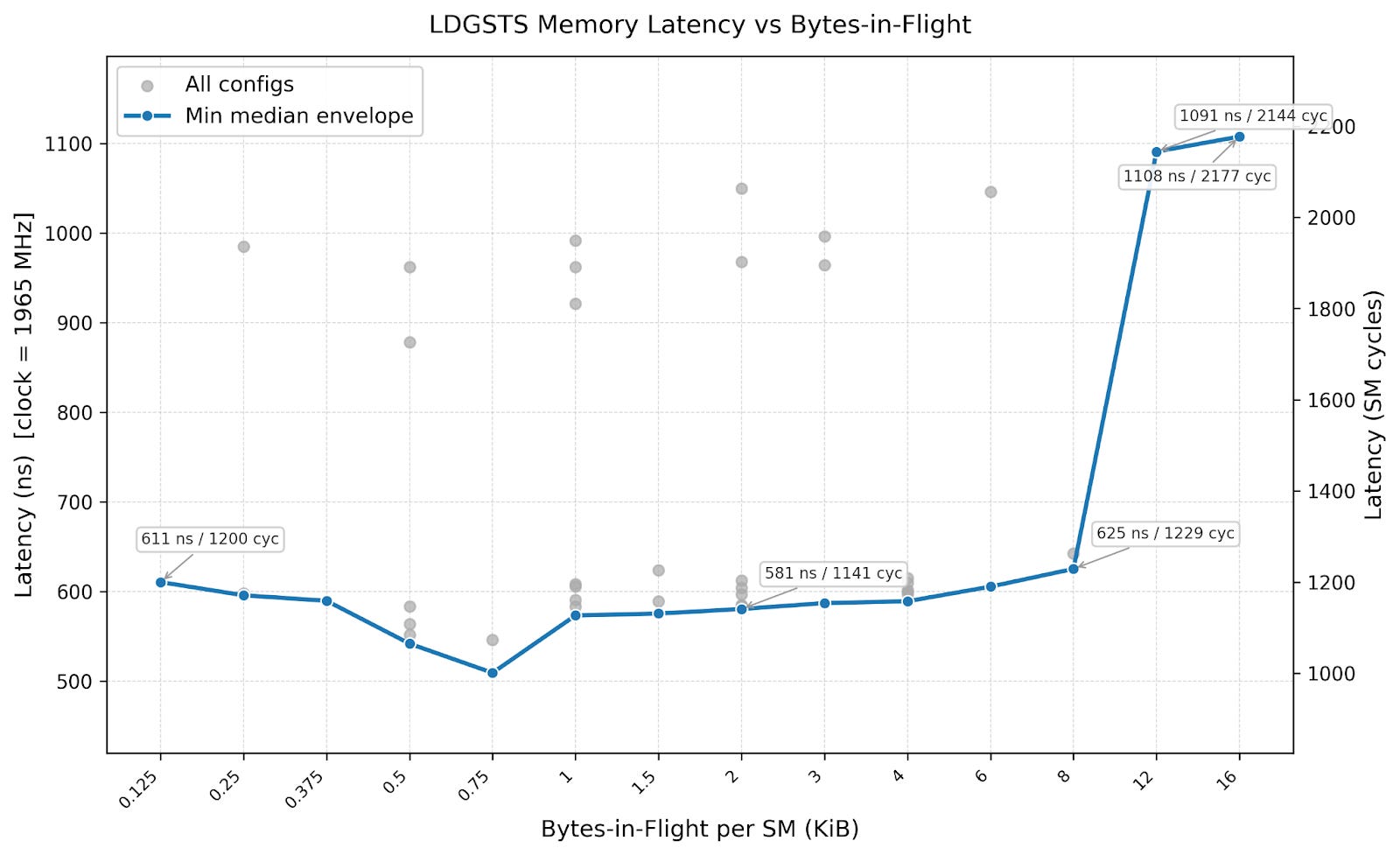
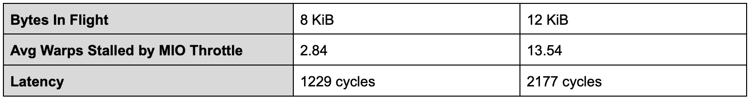
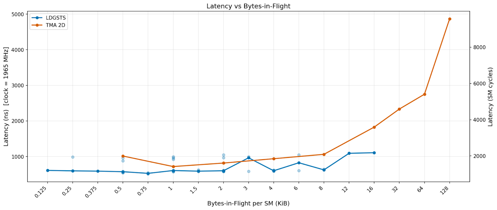
We benchmarked the latency of the same set of configurations. We see that LDGSTS has a baseline latency of ~600 nanoseconds and nearly doubles after 8 KiB in flight. This is because we need to use a large number of threads for LDGSTS to achieve high bytes in flight, leading to a high number of warps stalled due to MIO (memory input output) throttle.
Tensor Memory Accelerator (TMA)
TMA (PTX: cp.async.bulk.tensor, SASS: UTMALDG) is an asynchronous data copy engine introduced in the Hopper generation, specialized for moving large amounts of data from global memory to shared memory. A single thread can initiate TMA to perform address generation, memory swizzling, and out-of-bounds handling, freeing up other threads to execute independent work. Here we benchmark the 2D tensor version (cp.async.bulk.tensor.2d) to represent typical TMA usage.
Referencing FlashInfer attention kernels, we benchmark TMA, assigning only one CTA per SM but using one thread for each of 1 to 4 warps per CTA to issue TMA instructions of varying box sizes. The below graph shows the best-case throughput for each bytes-in-flight.
We benchmark TMA with the following configuration:
CTAs per SM: 1
Threads per CTA: 128 (4 warps)
TMA box dimensions: 2D shapes increasing from size 32x8 to 128x128
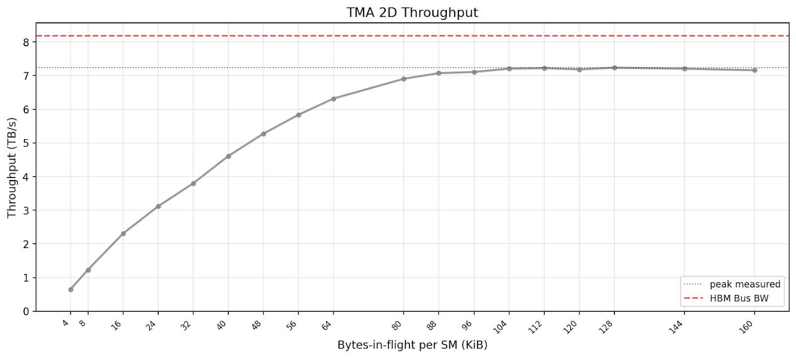
Peak throughput is reached far later than LDGSTS.
Async Copy vs. TMA Comparison
Deep learning kernel libraries like FlashInfer use both TMA and async copy for loading data. TMA and async copy have different performance characteristics: TMA is good for large loads with regular access patterns but has higher latency, while async copy can handle irregular memory access patterns but has size limits. We explain under what conditions we should pick one over the other. Here we benchmark the configurations FlashInfer uses for MHA and MLA kernels.
We see that throughput-wise, async copy slightly outperforms TMA at less than 32 bytes in flight, but TMA catches up after that and can continue scaling to 128 KiB. Latency-wise, we see async copy having slightly lower latency than TMA before 12 KiB in flight, but TMA latency greatly increases after that.
In reality, Blackwell MLA kernels use async copy for dynamically loading pages, while its MHA kernels use only TMA. Most of FlashInfer’s Blackwell MHA kernels are contributed by TRT-LLM, so we can only speculate what the kernels do by investigating the binaries. We found that similar to Hopper, all Blackwell TRT-LLM kernels use TMA. We suspect that for dynamic page loading, those kernels follow Hopper kernels, where they use 4D TMA with page index as the last dimension and index into the TensorMap object when needed. To understand the exact mechanics of the kernels, we urge NVIDIA to open source the FlashInfer TRT-LLM kernels for the benefit of the community.
TMA Multicast
TMA supports a multicast mode, where a single load copies data to the shared memory of multiple SMs, specified by a CTA mask. Multicast is commonly used in GEMM-like patterns, where input tiles are shared between SMs working on different output tiles. For example, multicast is useful for the activation function SwiGLU, which uses a dual-GEMM pattern of two GEMM operations sharing one input matrix. The major benefit is reducing HBM loads, which lowers effective bandwidth usage. It also significantly reduces L2 traffic, because requests for shared data for multiple CTAs are coalesced into one request.
According to NCU, the unit responsible for serving TMA multicast requests is called the L2 Request Coalescer (LRC):
The L2 Request Coalescer (LRC) processes incoming requests for L2 and tries to coalesce read requests before forwarding them to the L2 cache. It also serves programmatic multicast requests from the SM and supports compression for writes.
It sounds like the hardware might provide some multicast behavior, even if it isn’t explicitly requested, like a miss status holding register. We test this by running the same TMA multicast benchmark, except instead of one CTA issuing a multicast load, all CTAs issue independent TMA loads to the same data.
Here, we compare three cases:
Every SM loads different data (baseline)
TMA multicast (explicit) - one CTA in each cluster issues multicast loads to all CTAs in its cluster
TMA multicast (implicit) - all CTAs in each cluster issue plain TMA loads to the same data
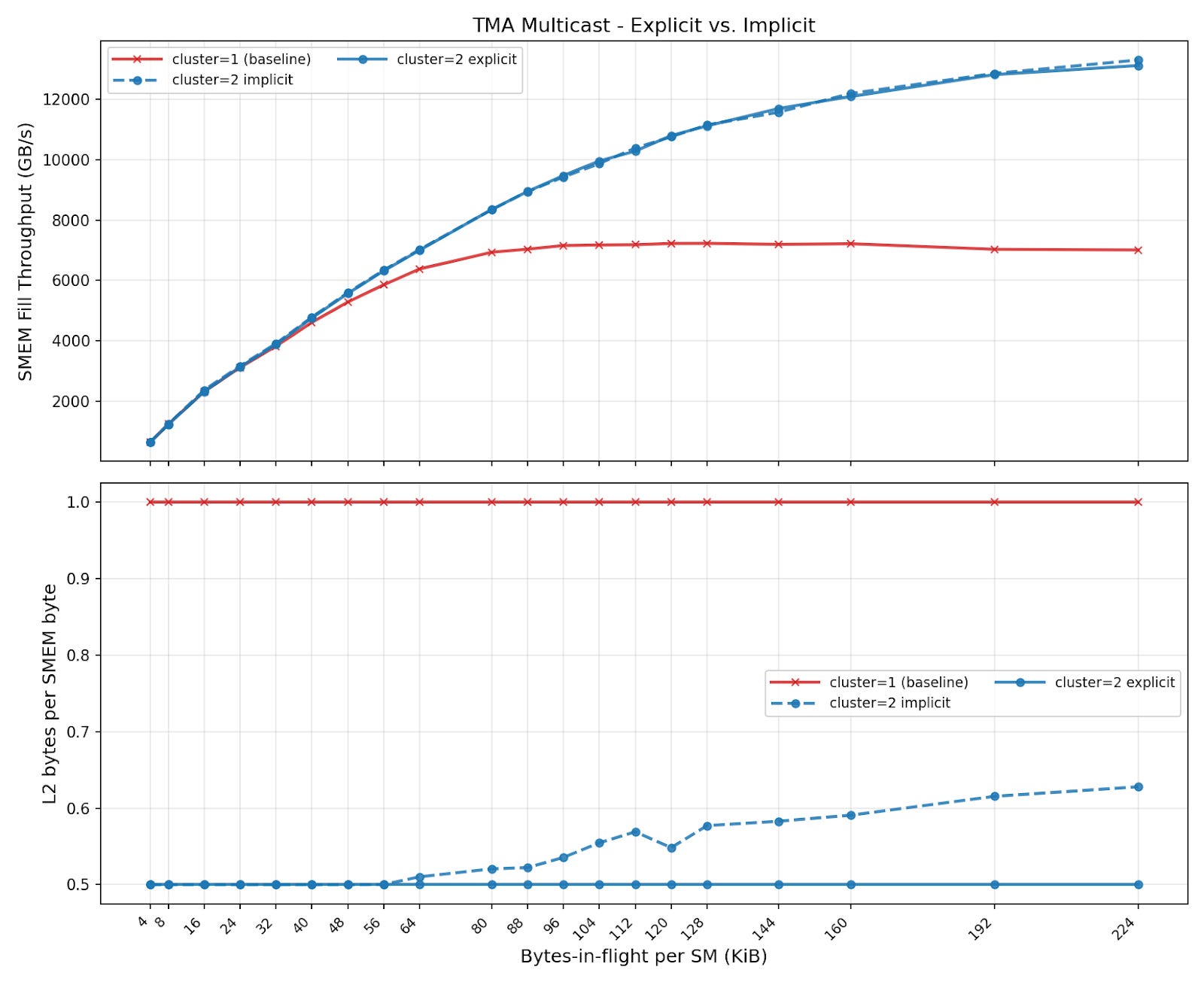
TMA multicast allows for much higher load bandwidth to fill SMEM buffers, even if data is not already in L2. For known traffic patterns, explicit TMA multicast instructions perfectly eliminate L2 traffic, resulting in the ideal “1 / cluster_size” L2 bytes per SMEM byte. We also observe that for this simple benchmark, we achieve nearly the same SMEM fill throughput in both the explicit and the implicit case. However, we can see the LRC is not perfect; the L2 receives a bit more traffic in the implicit case, especially as the total volume increases.
DSMEM vs. SMEM
NVIDIA introduced distributed shared memory (DSMEM) in the Hopper architecture. DSMEM allows CTAs within a cluster to access each other’s shared memory. This is useful for patterns like inter-CTA reductions. Reading peer-CTA memory through DSMEM has significantly lower throughput than SMEM’s 128 bytes per clock cycle.
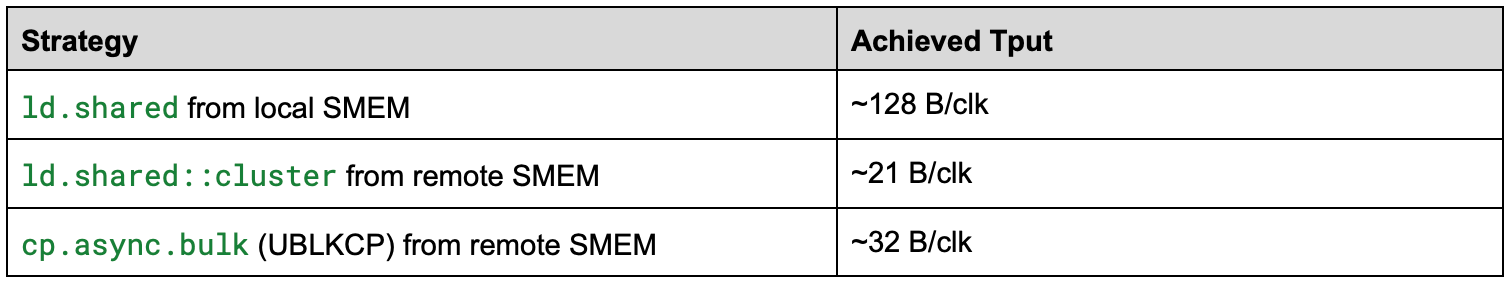
We experimented with a few different PTX patterns for interacting with DSMEM. An important difference when writing code for DSMEM vs. SMEM is that DSMEM loads are packetized similar to global loads, so the optimal access pattern looks nothing like the interleaved accesses that avoid bank conflicts in local SMEM, and more like a typical coalesced access to contiguous locations in GMEM. Additionally, we observed that in order to get the full 128B/cycle for local SMEM, `ld.shared` must be used without `::cluster`. This was a pitfall we ran into when we wrote a benchmark which simply used `ld.shared::cluster` to local and remote SMEM addresses. With `ld.shared`, the compiler emits `LDS` instead of a generic `LD` emitted with `ld.shared::cluster` which does not seem to be able to achieve peak throughput for local SMEM. We also struggled to push the achieved throughput further with `ld.shared::cluster`, and only achieved slightly higher throughput through DSMEM after switching to `cp.async.bulk`(PTX) / `UBLKCP`(SASS) to move higher volume of data per instruction.
The peak throughput we achieved when using each PTX pattern is below, expressed as bytes per clock cycle (B/clk) to align with the known max achievable in SM-local SMEM.
Tensor Core 5th Generation MMA
The MMA instruction is the core operation that performs matrix multiplication. MMA performance has grown increasingly shape-dependent from Hopper to Blackwell. Here we investigate this phenomenon, sweeping through different shapes and data types to quantify the performance differences.
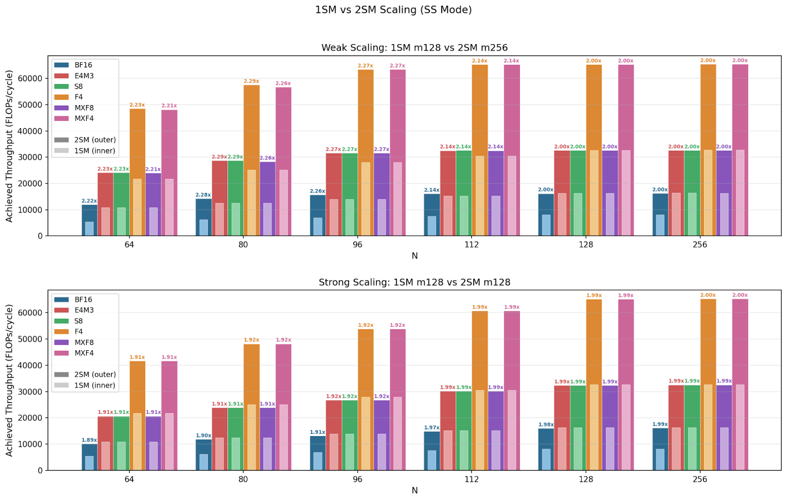
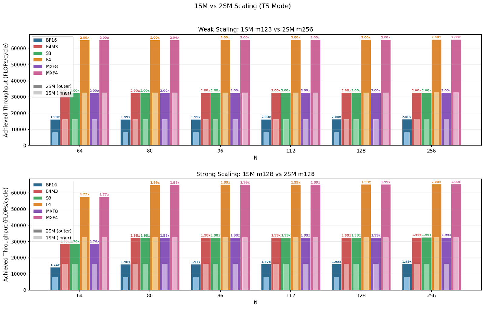
Blackwell comes with 2SM MMA, a new type of MMA instruction (.cta_group::2) where a CTA pair collaboratively executes one MMA operation across 2 SMs. Specifically, the input matrix A is duplicated while matrix B and D are sharded across the 2 SMs, and the CTA pair can access each other's shared memory. This enables even larger MMA shapes. We investigate whether 2SM MMA exhibits weak scaling, strong scaling, or both.
We benchmarked MMA performance with a configuration space below:
Throughput
NVIDIA claims specific throughput performance for different input data types, and here we show their claims for each (format + CTA group) and compare them with the max achievable throughput. We show that UMMA achieves near peak throughput for all formats and CTA groups, and even on 2SM versions where coordination overhead may be a concern.
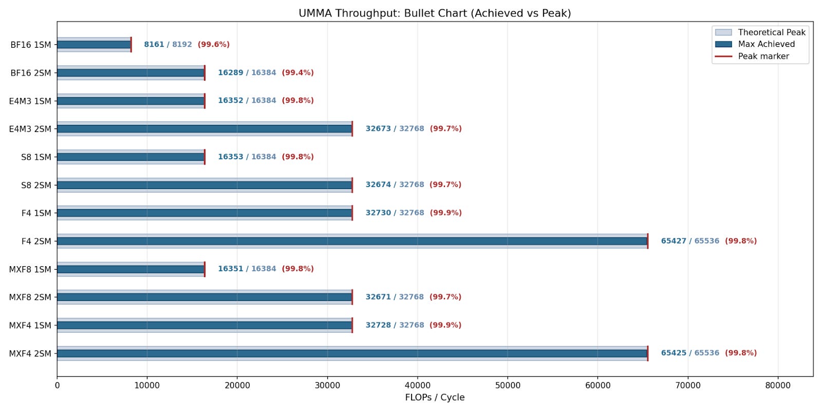
For 1SM MMA across all N sizes, we see that the smaller M=64 achieves max 50% theoretical peak throughput, and the larger M=128 achieves near 100%. This confirms that M=64 is utilizing half of the datapath. For 2SM MMA, we see that M=128 throughput starts at 90% peak for N=64 and reaches near 100% for all other N sizes. M128N64 throughput must be bound at a different hardware unit such as TMEM, L2, SMEM, etc. Meanwhile, M=256 sustains near 100% peak throughput across all configurations, this is because M=256 is M=128 per SM, which can utilize the full datapath. We note that throughput is identical across formats with the same data type bit width, and micro-scaling data types have virtually no overhead.
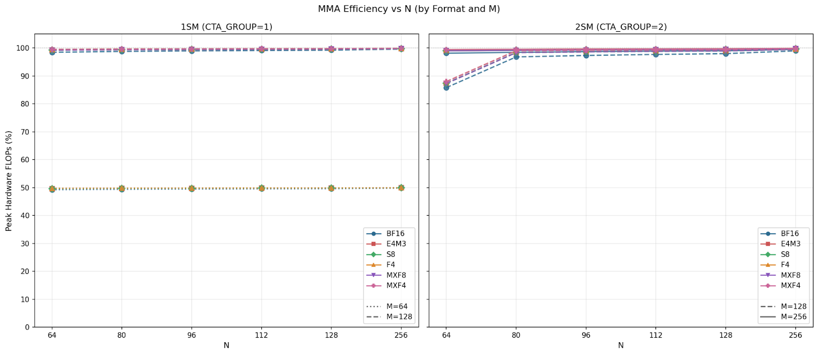
MMA supports two different AB layouts: Both input matrices stored in SMEM (SS), and matrix A stored in TMEM and matrix B stored in SMEM (TS). We observed that for M=128, while ABLayout=TS achieves near peak throughput, ABLayout=SS underperforms in smaller N sizes and catches up at N=128.
We can show that this is because the instruction itself is SMEM bandwidth bound below N=128 for SS mode. For example, for FP16 we know the hardware can do 8192 MMA FLOPs per cycle per SM, and the SMEM bandwidth is 128 B/cycle (per SM). So for M=128 N=64 K=16, we have:
A_bytes = 2*M*K = 4096; B_bytes = 2*N*K = 2048;
FLOPs = 2*M*N*K = 262144
SMEM Cycles = (A_bytes + B_bytes) / (128 B/clk) = 48 cycles
Math Cycles = FLOPs / (16384 FLOPs/clk) = 32 cycles
We compute this for increasing N and find we are finally Math limited starting from the N=128 instruction.
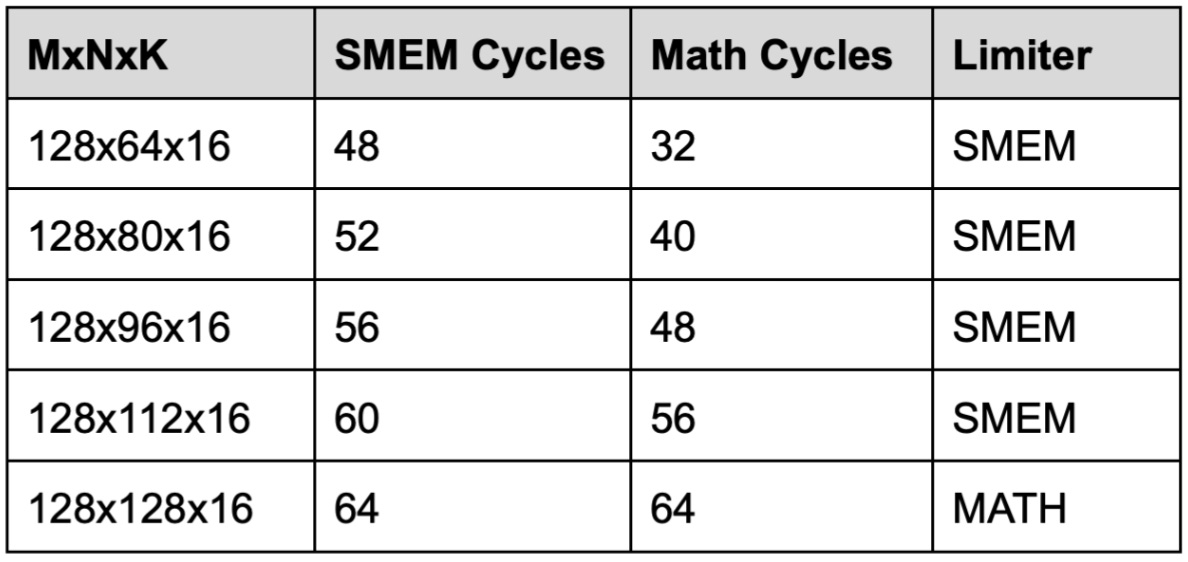
The same is true for other datatypes - MMA instructions with both operands in SMEM are SMEM-bound below N=128.
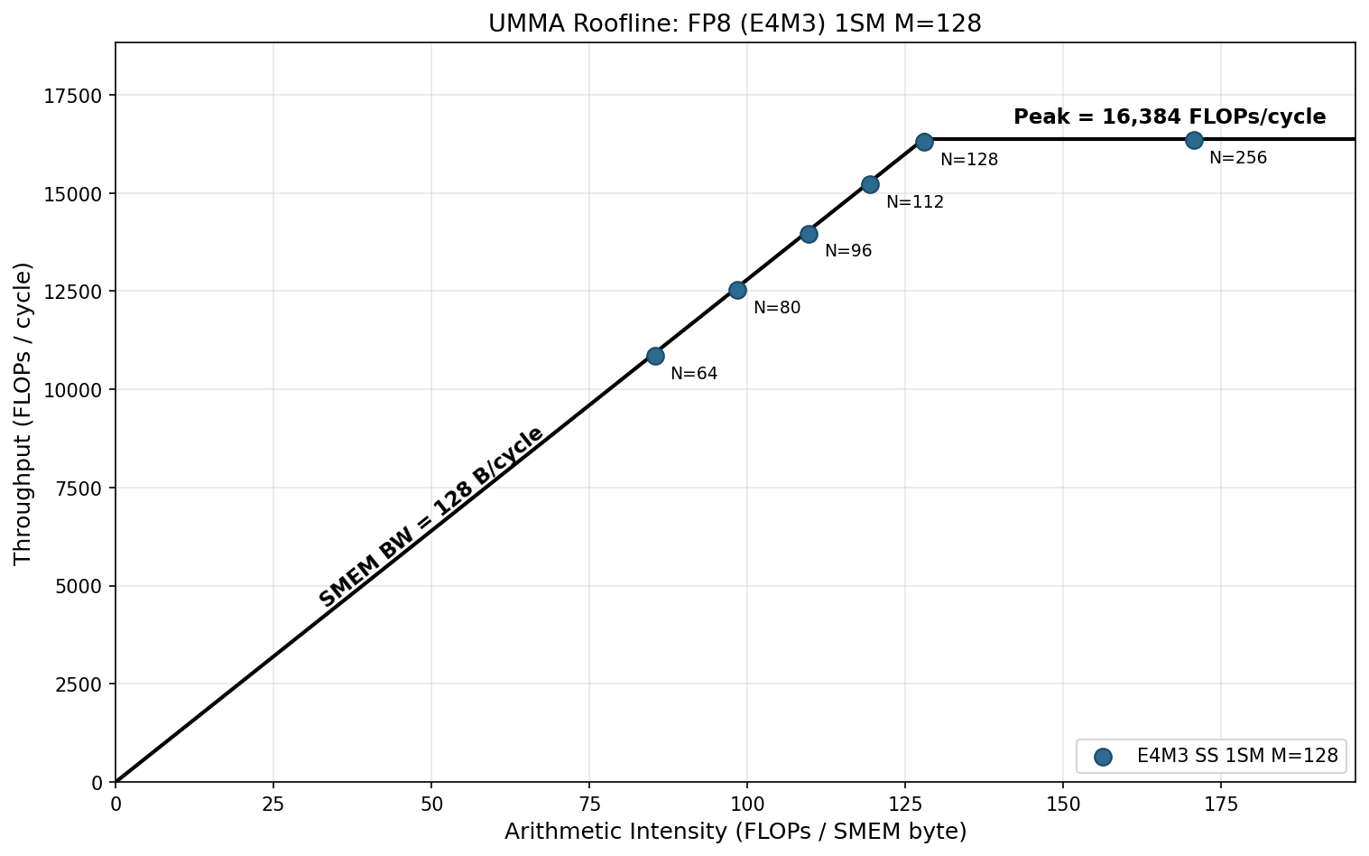
To further illustrate the point, we plot the roofline for all shapes of FP8 1SM MMA. We see clearly that the N < 256 is at the memory-bounded region, and the slope is roughly 128 bytes / cycle, the SMEM bandwidth.
2SM MMA achieves perfect weak scaling across all formats and shapes, reaching 2x speedup when using 2x the amount of compute resources than 1SM MMA. In smaller shapes of ABLayout=SS, we observe over 2x speedup, which again happens because the instruction is SMEM bound below N=128 for SS and the 2SM version splits operand B between the two SMs.
These experiments show that you should always use the largest instruction shape available for a given SMEM tile size to get maximum throughput.
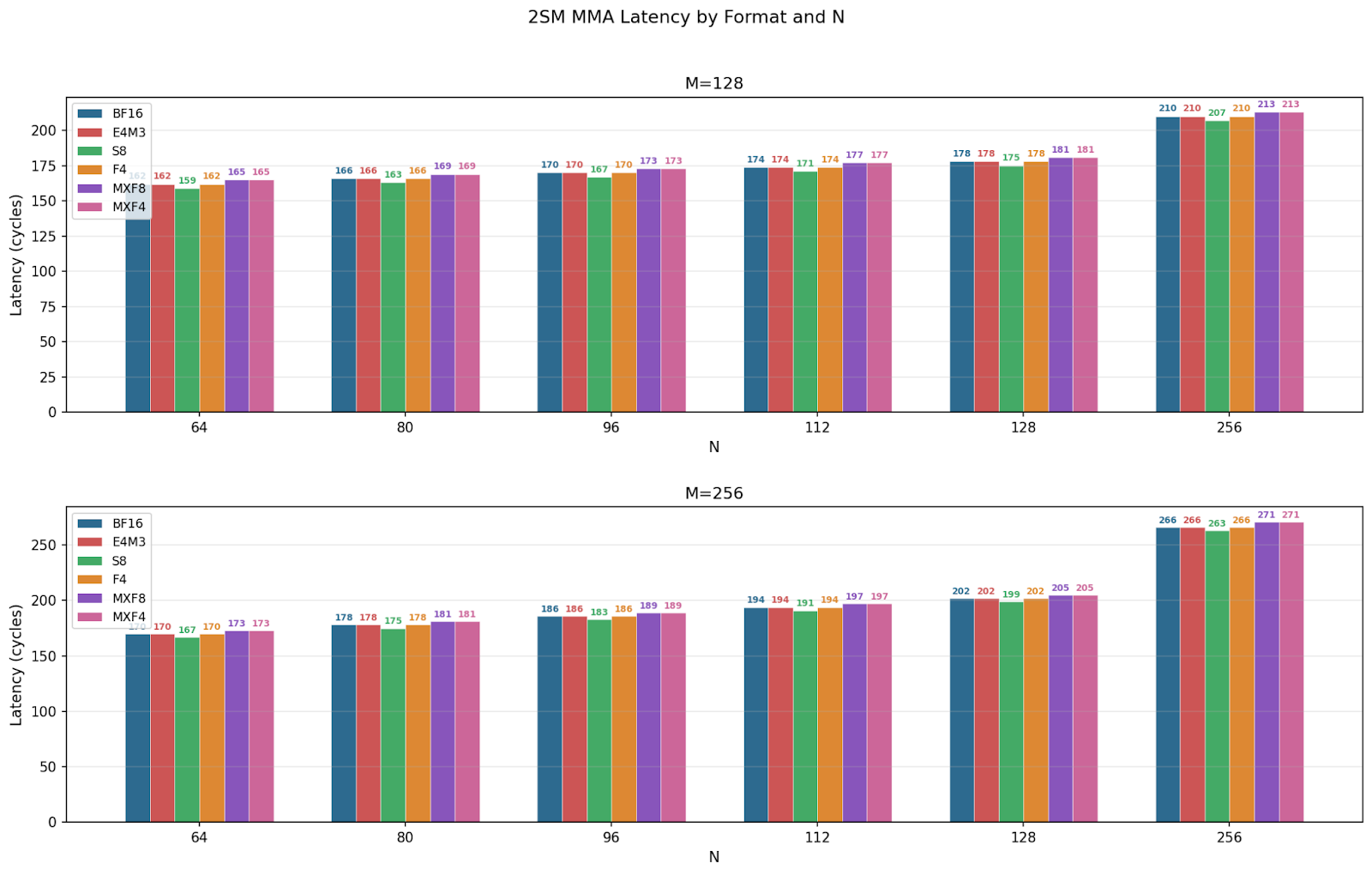
Latency
We benchmarked single MMA instruction latency, and we plot the comparison below. Across all configurations, we see latency linearly increases from N=64 to 128, and the spike at N=256 is likely due to the jump from 128 to 256. For individual CTA group MMAs, 1SM MMA M=64 and M=128 have similar latencies across N sizes, whereas in 2SM MMA, M=256 latency grows slightly faster than M=128, which matches our theoretical estimations. Comparing data types, we see little difference for 1SM but clear separation for 2SM MMAs.
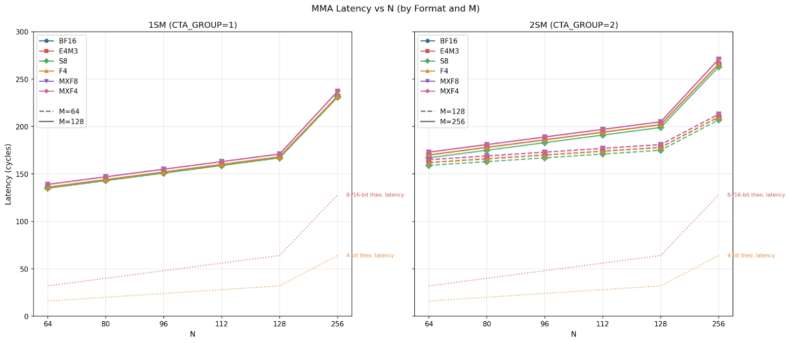
We notice a small but consistent pattern of the order of latency:
S8 < BF16 = E4M3 = F4 < MXF8 = MXF4
We believe integer operations being more power efficient leads to S8 being the fastest, and scale factor computation introduces a minor overhead for MXF8 and MXF4.
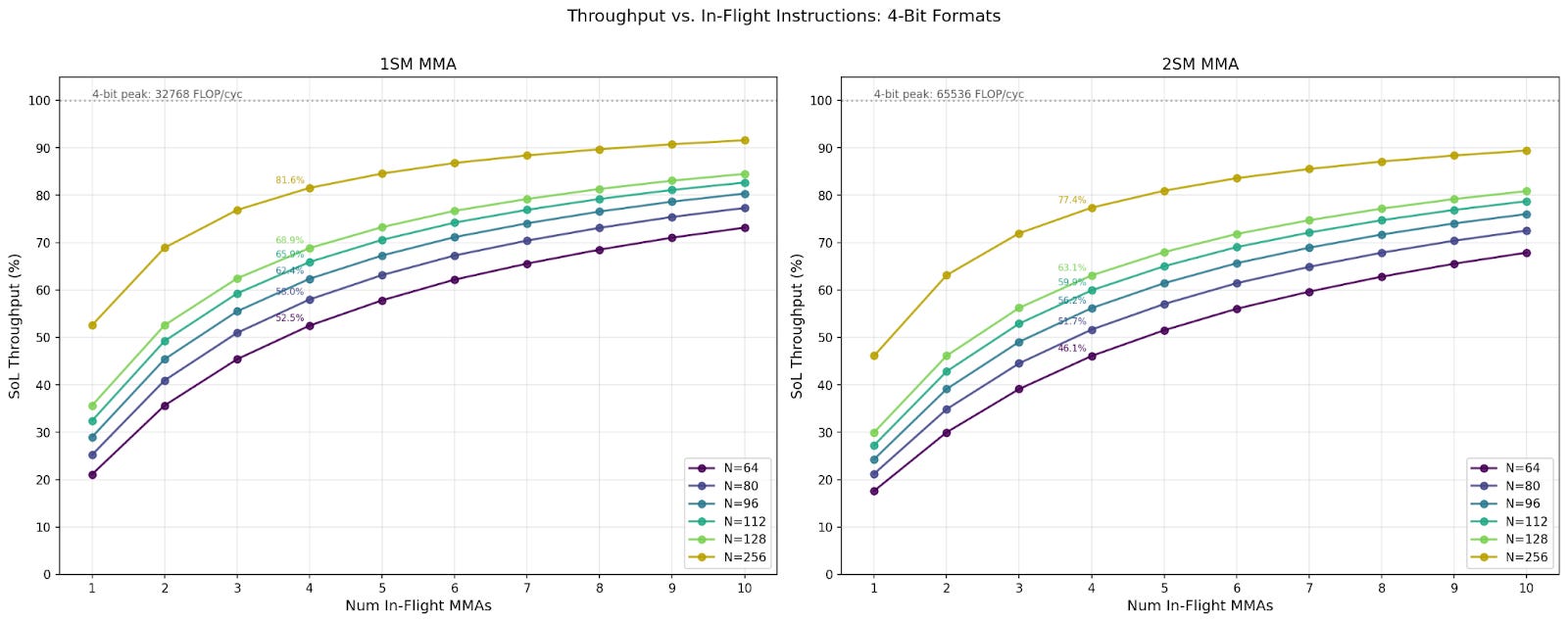
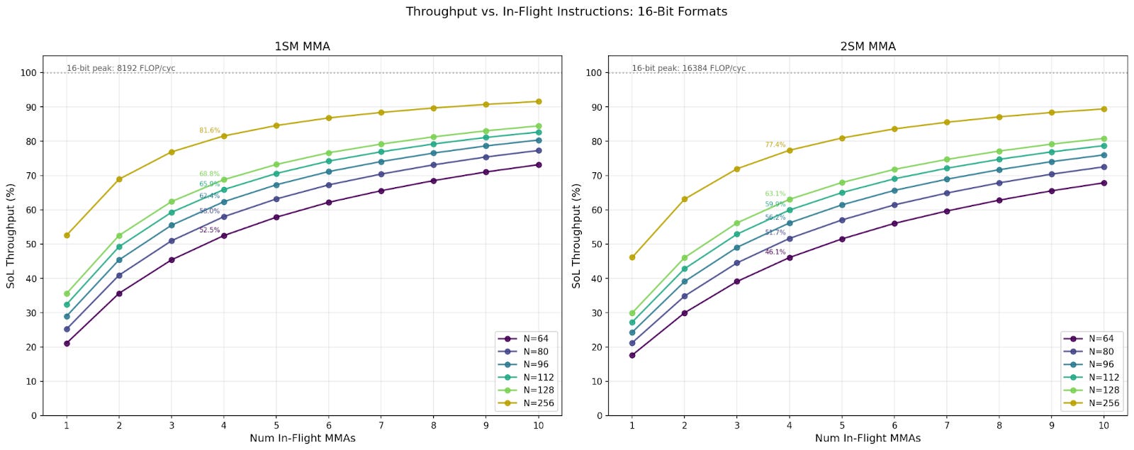
Throughput at Different In-Flight Instruction Count
In our throughput benchmark, we set high numbers of in-flight instructions to amortize instruction issuing and commit wait overheads, ranging from 256 to 1024. However, kernels typically use 1 to 4 in-flight MMA instructions. We benchmarked the throughput at 1 to 10 in-flight instructions, and we discuss the changes in throughput here.
Across all configurations, we see the same N and in-flight MMAs achieve similar percentages of Speed-of-Light (SoL). Notably, only the largest N reaches 90% SoL, while the smallest N achieves only about 70%. Comparing 1SM and 2SM MMA, we see 1SM achieves around 5% higher SoL throughput than its 2SM counterpart. For the same data format and CTA group MMA, the throughput for larger N is always higher than smaller N sizes. Finally, we observe that the throughput SoL percentages for 4 in-flight MMAs caps out at 78% - 80%.

Below we discuss real-world use cases with kernel writing library CUTLASS. We also discuss throughput, multi-cast, and floorplans.