How to Kill 2 Monopolies with 1 Tool
Substrate X-Ray Lithography, a New American Foundry, $10k Logic Wafers
The chipmaking industry is, surprisingly, ripe for disruption. Technical decisions at incumbents are often driven by inertia, “that’s what we’ve always done.” Regression is feared above all else. Something as simple as fab lighting color cannot be changed: traditional yellow lights are still used in photolithography lines even though fabs will readily tell you it no longer has any risk of affecting the photoresist.
This has worsened in recent years. Chipmakers iterate on existing technology despite slower scaling and rapidly increasing costs. ASML has a tool on their roadmap, hyper-NA, that they openly admit may not be economically viable! But it’s hard to fault these companies – the tools and fabs print a lot of money. A single EUV tool, sold for $225M, can produce more than $650M in complete wafers in a year (note that there are many costs beyond that single EUV tool incurred in producing those wafers). There is little incentive for incumbents to change tack.
But that leaves an opening for masochistic bold, scrappy innovators… enter Substrate.
X-Ray Lithography
Substrate is a recently out-of-stealth Bay Area startup inventing “technology to power next-generation foundries” with the mission to substantially reduce the cost of advanced logic wafers. The first major step towards this mission is a new X-ray lithography (XRL) tool that the company has invented.
The idea of x-ray lithography has been around for half a century. MIT researchers produced the first functioning devices using XRL in 1972. Most labs doing lithography research at least experimented with it - Bell Labs, IBM, and others. IBM even built chips using XRL in the 90s, but long wavelength (DUV and above) techniques kept scaling, so there was no need to overcome the numerous challenges facing XRL. Chief among them are (a) optics, since just like EUV, almost nothing bends nor reflects X-ray wavelengths and (b) sources, since generating a bright, isochromatic, and stable source of soft X-rays typically requires massive particle accelerators.
The fields of spectroscopy and microscopy continued ahead with soft x-ray technology even after chip industry interest moved elsewhere. High quality research-grade optics and ‘tabletop’-scale sources have been a focus of intense research, but nothing resembling a leading edge lithography system has gone public.
It appears Substrate has overcome these x-ray challenges at least partially, and their performance claims are stunning:
Single-patterning capable for all layers at 2nm, 1nm, and possibly nodes beyond
Equivalent resolution to high-NA EUV
12 nm features demonstrated
Capable of complex, arbitrary patterns
Overlay <= 1.6 nm, full-wafer CDU 0.25 nm, line edge roughness (LER) <= 1 nm, LCDU <= 1.5 nm
Leading edge wafers will be produced at 50% less than existing options
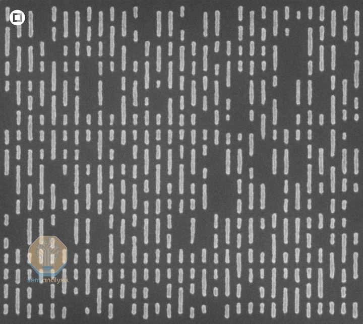
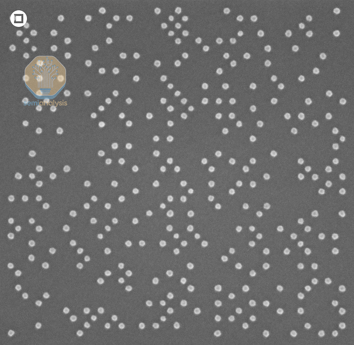
These are extraordinary claims and thus demand extraordinary evidence. Let’s take them one-by-one:
Single-patterning for 2 nm, 1 nm, and beyond: the line/space pattern is 12 nm lines + 24 nm spaces, which add up to P36. The target for 2 nm - 1 nm nodes is more like the P20-22 range, but it’s not clear this pattern was targeting minimum total pitch. Tip-to-tip distance between line ends is 13 nm, very good for single patterning.
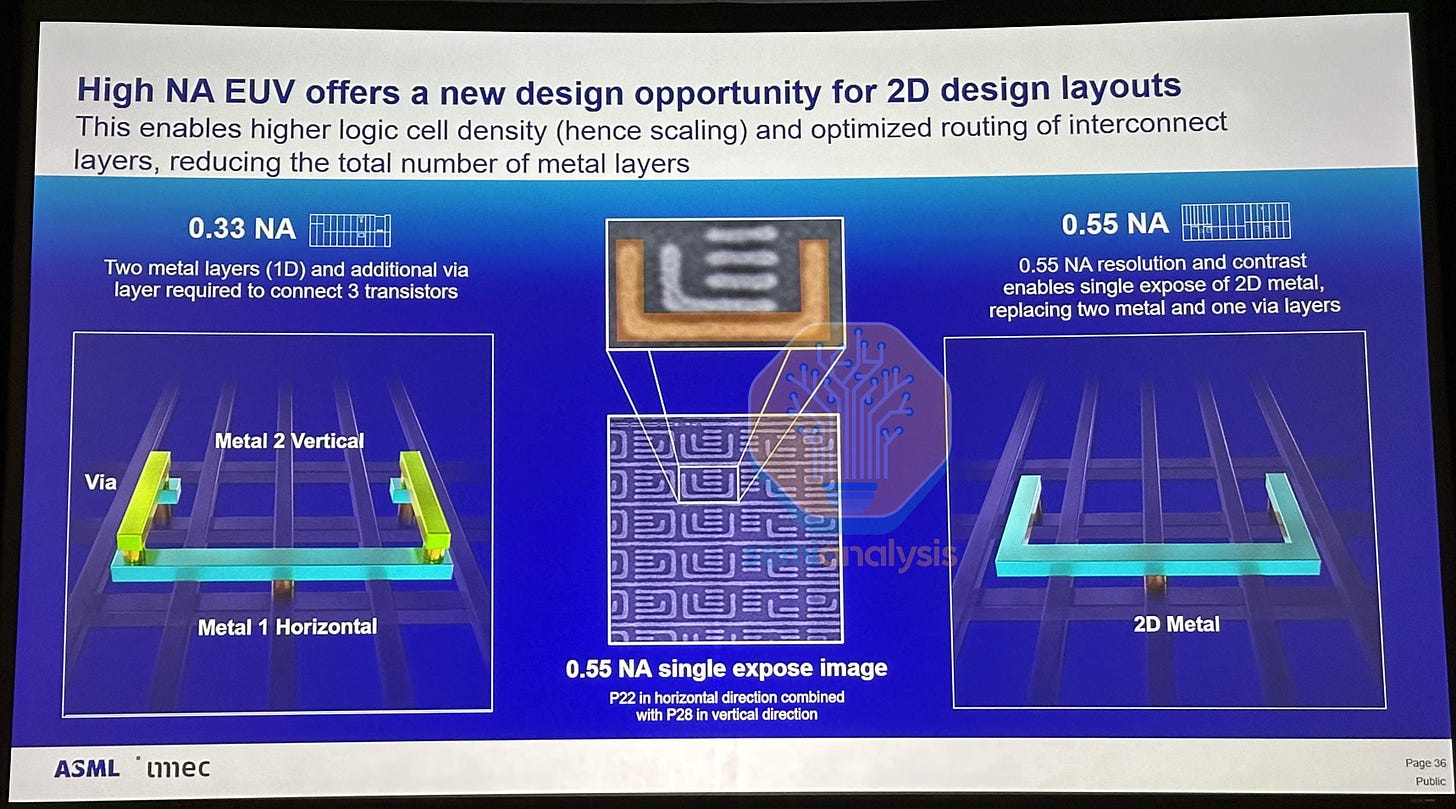
Still, this is clearly in the high-NA class of single patterning resolution where low-NA is limited to ~P28. And the random vias look very good, 30 nm pitch is aggressive.
Complex, arbitrary patterns look to be true. Micrographs of bi-directional patterns have not been publicly shared, but an example of dense structures was shared with us. The results are promising, but here is a lot more we need to see and understand. The expected patterning challenges at this scale and density are clearly present (LCDU, stochastics, etc). It’s also not clear if this was a resist or etched pattern.
Overlay 1.6 nm is high for critical layers in the most advanced logic processes. A good heuristic is overlay = 10% of feature size, so closer to 1.0-1.2 nm would be ideal in this case. It’s not clear if this is machine-matched overlay, which is much more difficult that single-machine but important for high volume fabs. Good machine-matched overlay allows you to run successive layers on different litho tools, simplifying production planning in the fab. ASML achieves ~0.9 nm machine-matched overlay on the latest EUV machines.
Full-wafer CDU of 0.25 nm is exceptional. It’s actually beyond typical measurement capabilities. Assuming both are measuring the typical 3 standard deviations of the mean CD for each field, this is much better than the 0.7 nm on ASML’s 3800E scanner.
Good CDU means more consistent performance in the end chip – a transistor on one end will have similar threshold voltage, drive current, etc. as one on the other, for example. It also improves yield as CDs are more likely to be within the design tolerance.
Leading-edge wafers will be 50% cheaper than existing: this remains to be seen. Presumably this is done mostly via eliminating multipatterning and reducing single-exposure costs. With the most favorable assumptions, a detailed SemiAnalysis model of a 5 nm-class process shows a 25% cost reduction. A 2 nm process would not be substantially different. It may not match the claim, but a 25% savings is massive in this context and would mean a substantial competitive advantage.
Evidence so far is scarce, so we repeat these claims with some healthy skepticism. But we should also note, external contacts and 3rd party reports are all telling us the same story: the litho tool is legit. Note we have worked with Substrate since as far back as 2022, but the technical analysis here was by team members who did not have access to that NDA information.
Substrate isn’t stopping there. They intend to run the tools in their own fabs rather than sell to 3rd parties. The mission isn’t just XRL, it’s a new American foundry. The goal is to develop an entire end-to-end chipmaking process, buying off-the-shelf when suitable options exist, inventing when they don’t.
Key to this is lithography using a large synchrotron, particle accelerator, or free electron laser that is on the scale of entire fabs to generate sub-EUV wavelengths. While Substrate has long since decided what they are doing, they want to keep it vague for competitive reasons. Note the cover photo of this report is purely AI generated and not what it looks like.
Naysayers will point out a million reasons why this is improbable, difficult, etc. - and they are mostly correct. There is a big difference between lab-scale and industrialized, high-volume tools. Substrate itself realizes this and agrees they are in for a lot of development and scaling pain.
Still, they have at least developed some impressive capabilities on the most complex part of the process (litho) in a short amount of time (2-3 years). Let’s assume the claims about the XRL tool are correct. What are the implications?
If True, How Does XRL Affect the Industry?
The answer is similar to what you’d say if a high-NA tool cost <<$40M rather than $400M. In short, it revolutionizes lithography.
It would open the floodgates in process node design flexibility. Continued device area scaling would no longer be limited by lithography cost but on transistor design, materials and electrical characteristics.
Take one example: the M0 layer. Typically, pitches of the lowest metal layer (M0) and tip spacing between gates and M1 lines define how compact a process node’s standard cells can get, with tighter M0 pitches and spacing correlating to higher transistor density.
Current 23 nm M0 pitches from TSMC already rely on multi-patterning with low-NA EUV with additional cut masks to achieve close tip-to-tip spacing. Intel’s 32 nm M0 on 18A uses with single patterning low-NA and pattern shaping tools to narrow T2T spacing, with backside power delivery allowing a one-time relaxation of M0 pitch. We are not expecting M0 for their 14A node to go below 26 nm given the modest area scaling targets, which allows them to deploy high-NA EUV single patterning in a cost-effective manner with assistance from Directed Self Assembly.
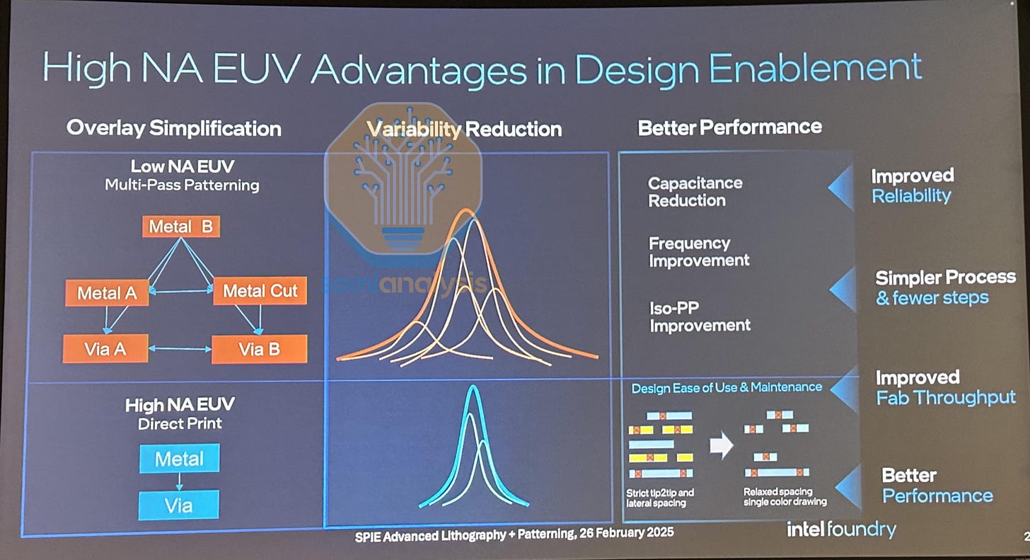
With Substrate’s tool, multi-patterning complexity can be replaced with a single exposure while also freeing up many design rule restrictions on metal line placement. Area scaling could be more aggressive to offer dense low power libraries for mobile and AI accelerators. At 20 nm metal and 30 nm via pitches, the 1 nm-generation process nodes for 2030 could stay at single exposure with Substrate’s tool.
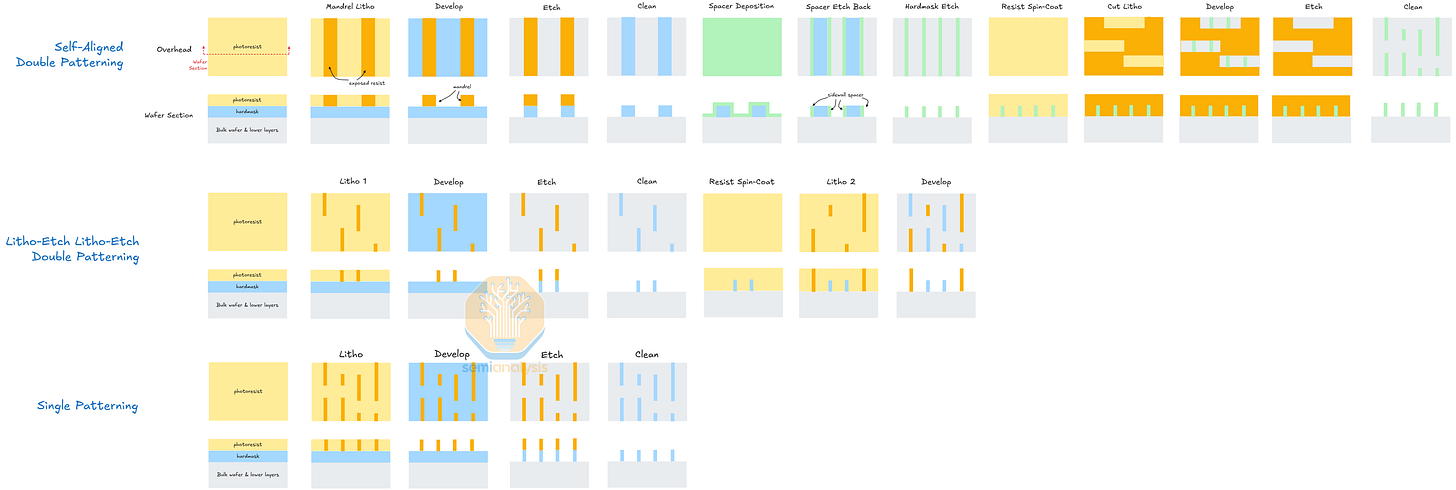
ASML and others have repeatedly made the case for high resolution single-patterning being preferable to multipatterning. It does, as they say, reduce complexity. It does not, by default, reduce cost. When the litho tool like the ASML EXE:5000 (High-NA) is $400M, the economics don’t work. When the tool is $40M (this is the correct order of magnitude for the Substrate XRL, not an exact number), the economics work really, really well.
Substrate’s cost advantage claims go further than just high-NA:
Substrate’s X-ray lithography is so cost effective that we are capable of printing every single layer in an advanced process, including larger pitch DUV layers, while maintaining high tool and facility throughput
IF true and IF Substrate pivoted to 3rd party sales, ASML is in serious trouble. This is a TAM in the $50B range by 2030. But again: there is a long way to go between lab-scale and high-volume tools.
Challenges Beyond Litho Resolution
Improved litho resolution is also not a panacea. Advanced logic scaling now depends as much on materials engineering and other processes as it does lithography.
Even within the patterning process itself, there are many fundamental challenges. We note these not to say that Substrate can’t overcome them, but just to give an idea of how monumental this hill is to climb:
Even with a shorter-wavelength tool capable of resolving a target pitch in a single exposure, multipatterning techniques like SADP and LELE may still be preferred for reasons beyond simple pitch splitting…
Process Control and Quality Improvement: Self-aligned processes offer inherent advantages in pattern fidelity. SADP provides superior control over Line Edge Roughness (LER), Line Width Roughness (LWR), and Critical Dimension Uniformity (CDU). This is because the final critical dimensions are defined by highly controllable deposition and etch steps, not solely by the lithographic aerial image. These steps can be actively tuned to reduce roughness; for instance, optimizing thin film stress during spacer deposition or adjusting etch plasma chemistry can smooth features and reduce line “wiggling”. In essence, SADP can correct for imperfections in the initial lithography step, potentially producing a higher quality final pattern than a direct, single-exposure print.
Stochastic Defects: As wavelength shortens, photon energy increases (EUV at 13.5 nm is ~92 eV; B-EUV at ~6.5 nm is ~190 eV). To maintain a constant exposure dose, far fewer photons are required. This dramatically increases the statistical “shot noise,” where random fluctuations in the number of photons hitting a feature can cause it to fail to print (a missing contact) or bridge to a neighbor. This effect is a primary cause of random defects and represents a potential hard wall for scaling. The estimated shot-noise-induced roughness for EUV is already significantly higher than for 193i lithography, and this trend is expected to worsen at shorter wavelengths.
Secondary Electron Blur: High-energy photons (EUV and X-ray) do not directly cause most chemical changes in the resist. Instead, photon absorption creates a high-energy photoelectron, which then generates a cascade of lower-energy secondary electrons that travel through the resist, causing the actual chemical reactions. This travel distance creates a “blur” around the initial photon absorption point. For X-ray lithography, this secondary electron blur is a known fundamental resolution limiter that broadens as the incident photon energy increases.
Design and Process Window Flexibility: For complex two-dimensional layouts, Litho-Etch-Litho-Etch (LELE) provides greater design freedom than the unidirectional constraints of SADP. Decomposing a complex pattern into two simpler, less dense masks can also enlarge the process window for each individual exposure, though bringing plenty of its own challenges. Printing a single, highly complex pattern pushes optical proximity correction (OPC) to its limits and is more susceptible to “hot spot” defects and corner rounding, whereas two simpler exposures can be more robustly manufactured. That said, LELE has great challenges of its own with scaling, namely EPE, alignment and overlay, which may be reduced by collapsing the number of passes. More recent implementations like SALELE again break the ability to pattern arbitrary structures.
High-Aspect-Ratio (HAR) Etching: Etching deep narrow trenches, for example to isolate GAA Si/SiGe when producing channels (~10:1 aspect ratio), is limited by ion transport to the trench bottom and byproduct removal. This can cause “etch stop” or profile distortions like bowing, which impact device performance regardless of the initial pattern’s quality.
Selective Etching: This is a materials science and surface chemistry problem that cannot be solved intrinsically by better lithography.
Line-Edge Roughness (LER) Transfer: LER from the photoresist can be amplified during the plasma etch transfer process. A perfect lithographic pattern is negated if the subsequent etch roughens the final feature.
Edge Placement Error (EPE): EPE is the total deviation of a feature’s final edge from its intended location, with a budget in the low single-digit nanometers for the 2 nm node. It includes litho overlay, mask errors, CD variation, and etch biases. A perfect lithography tool cannot correct for non-linear wafer distortions induced by previous high-temperature process steps. Even self-aligned processes like SADP ultimately require a separate, critically aligned “cut” mask, reintroducing a major source of EPE.
X-ray Damage: X-rays can penetrate the resist and hard mask, causing damage to existing structures. Even low energy X-rays can damage gate dielectrics and doped Si regions, both critical to a performant transistor. X-ray exposures on layers above existing devices will need to be extremely well controlled.
Beyond Litho Implications
We could make a similar list of obstacles in developing a full process technology node, but you probably get the idea at this point. Let’s go back to the implications if things work out:
If Substrate can achieve their stated goal of leading edge wafer production at 1/10th the existing cost, this of course means taking market share from TSMC. That alone will be an addressable market of well over $200B in 2030. But reducing chip costs by an order of magnitude would have much larger consequences than eating into TSMC share.
In the absolute best-case scenario, this is an end of decade story. In broad strokes, it will take another 2 years to mature the process technology such that customers can begin design work. Design and tape-out work is another year, and then ramp to volume is 1 more year. This would be ludicrous speed for the existing industry workflow. Substrate’s goal is to upset the paradigm and speed up these cycles, with tape-outs as soon as 2028. We will see.
Strategic Implications
An American firm producing cutting edge lithography tools, and possibly cheap advanced chips, vastly improves the U.S.’ strategic position. We’ve argued before that the risk concentration in Taiwan fabs is extreme, and that advanced chipmaking capabilities must be on-shored. Seven American mega-caps depend almost completely on TSMC Taiwan for nearly $2T in annual revenue!
Substrate adds a 3rd arrow in the on-shoring quiver. TSMC is expanding rapidly in Arizona, but will not build the most advanced nodes there and still does R&D in Taiwan. Intel is doing R&D and HVM in the U.S. but hasn’t delivered a competitive leading edge node in the last decade. Samsung is even further behind Intel. Substrate is attempting it from scratch, which historically has not had great odds. At any rate a 3rd option is a positive for the U.S.
Naturally, China will be paying attention. Their ecosystem is basically trying to do the same thing as Substrate – develop an advanced logic ecosystem from scratch – but with nation-state-level resources behind them. EUV is, of course, the most important export controlled chipmaking tech. Substrate XRL will no doubt attract imitators and espionage the same as EUV.
For that reason Substrate is taking extreme care to protect its innovations. You’ll notice that we’ve written basically nothing here about how the XRL tool works; it’s because they are making almost nothing about it public to prevent theft of the trade secrets. Note we have worked with Substrate since as far back as 2022, but the technical analysis here was by team members who did not have access to that NDA information.
The company is also strongly committed to avoiding the mistakes of the EUV program. Much of the fundamental IP underlying today’s commercial EUV tech was developed in the U.S., first by national labs and then the public/private consortium EUV LLC. ASML won the battle for licensing, in part by acquiring the American firm Silicon Valley Group. Although it wasn’t obvious at the time, the U.S. allowed “crown jewel” technology to be sold out of the country. ASML no doubt did much of the hard work to industrialize it over the next 2 decades, but it should’ve been an American firm instead. We clearly cannot allow the same thing to happen with a potential successor to EUV, especially with China hot on the trails with similar attempts.
Competitors
Comparisons naturally come up with xLight, a startup attempting to build and commercialize free electron laser (FEL) light sources. Both Substrate and xLight’s devices are capable of sub-EUV wavelengths, but that’s where the similarities end.
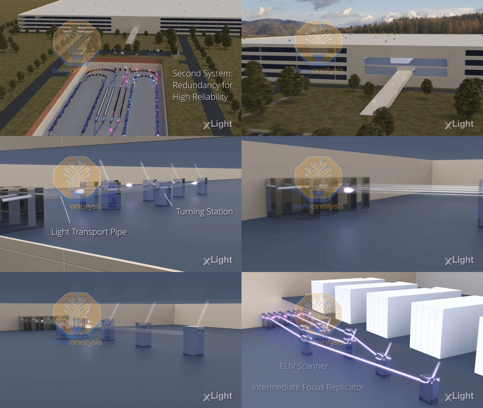
xLight is producing only the litho light source, using a novel technology. Theirs is meant to plug in to an existing EUV tool in lieu of the ASML laser-produced plasma source. They are in the process of building the first working prototype, but if proven, the FEL source will mostly offer an evolutionary step in EUV performance (overall tool performance will increase but run into other limits like stage movement speed and mirror heating).
Substrate XRL is, if proven, a revolutionary step in lithography performance in cost per wafer. It uses a proven light source technology with a novel exposure tool, opposite xLight. The business models are also quite different – sell to existing fabs via ASML for xLight, operate as part of their own process in their own fab for Substrate. xLight has not exposed any wafers while Substrate, via U.S. national labs, has.
China also has multiple major similar efforts in this domain as well. While they do not have functioning ArFi DUV still, they should in the coming years and they are already working on EUV, High-NA EUV, and XRL via multiple different teams / efforts including cool FEL / particle accelerators / syncatrons just like xLight and Substrate.
Next Milestones
Most of this report is based on the promise of Substrate. A novel demo tool with these imaging capabilities built in 2 years is impressive. But there is a lot more to prove before they disrupt the chipmaking industry. We're hopeful for success but skeptical given how many questions there are. We’re looking forward to a few milestones that will silence the skeptics (both internal and external):


