

Interconnects Beyond Copper, 1,000 CFETs, SK Hynix Next-Gen NAND, 2D Materials, and More
IEDM 2025 Round-Up
It’s an odd time in the chipmaking industry. On one hand, we are ramping into the biggest supercycle ever seen. Advanced logic, DRAM, NAND, customers can’t get enough, chipmakers can’t build capacity fast enough, and we may soon be limited by fab equipment supply. On the other hand, the rapid technology improvement in scaling, power consumption, chip cost, etc. have slowed to a crawl. Massive research efforts yield small incremental gains. As costs increase but improvements asymptote and scaling runs out of room at the bottom, it sometimes feels like Moore’s Law has become Moore’s Wall.
The good news is the semiconductor industry has a long history of making naysayers look stupid in the long run. There are plenty of innovations on the bench that are promising for the next decade and beyond. In this report, as with 2022, 2023, and 2024, we’ll cover highlights from IEDM 2025 to find out what the future of chipmaking might look like.
With memory prices exploding, 3D NAND technology is suddenly relevant again. We’ll look at the technology and competitiveness of SK Hynix’s latest V9 NAND, Samsung’s use of Mo to improve its existing V9 products, and a big innovation that we may see in future production from SK Hynix. For advanced logic, we’ll look at interconnect metals beyond Cu, the potential of 2D materials to replace Si in transistors, and the progress in CFET, the next big inflection after gate-all-around.
3D NAND
NAND scaling is critically relevant right now, as demand is spiking but there is no cleanroom space for building out capacity. Memory producers are limited to upgrading existing lines, so their supply is constrained by how dense their upgraded process is. For leading fabs, this is a 3xx-layer 3D NAND process, which yields on the order of 20-30 Gb/mm2 of memory. That pencils out to 30+ TB of memory on a single 12” wafer (note the difference between (b)its and (B)ytes in these abbreviations).
3D NAND: Hynix 321 Layer
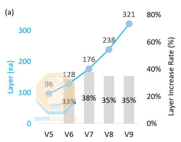
In the case of SK Hynix, the 321-layer process has 44% more memory per wafer than the previous generation 238-layer technology. If you are constrained by cleanroom space and by extension the number of wafers you can produce, 44% more memory on each of those wafers makes upgrades an obvious choice.
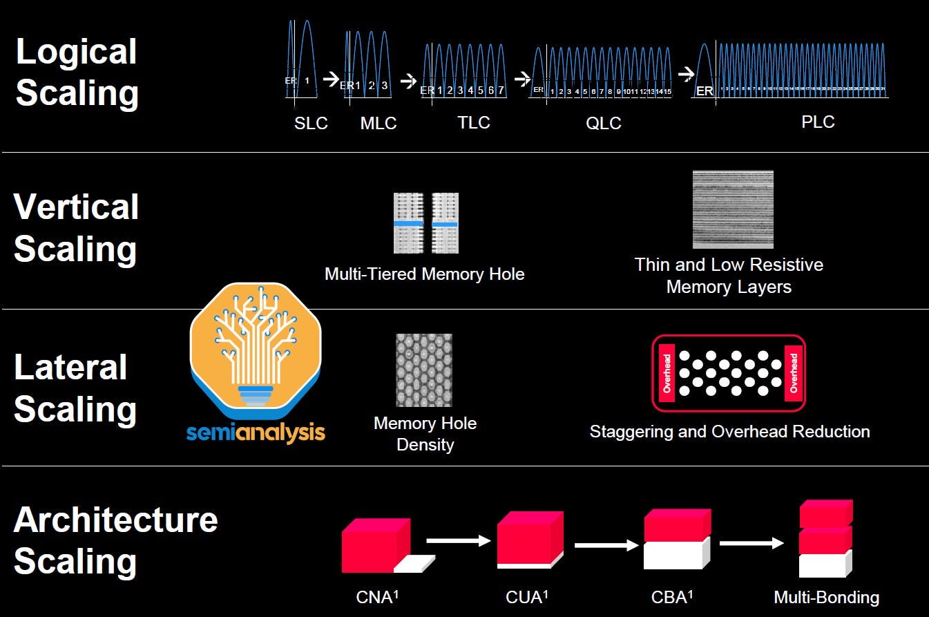
We’ve written in detail about NAND scaling methods, as a quick recap:
There are 4 main avenues for scaling the storage capacity of NAND Flash per wafer.
1. Logical scaling – The number of bits stored per cell. This requires storing 2^n voltage levels per cell.
2. Vertical scaling – The number of NAND cells stacked vertically
3. Lateral scaling – The size/number of cells that can be fit on the 2D vector
4. Architecture scaling – Various techniques to increase density and reduce overhead from cells/periphery.
Remember that NAND is just about cramming as many storage cells onto the wafer as possible. This manifests in 3D NAND as vertical cylinders, channels, packed tightly together like trees in a forest. Flat layers, alternating between conductive and insulating material, surround these channels. A memory cell is formed at each intersection of channel and conductive layer.
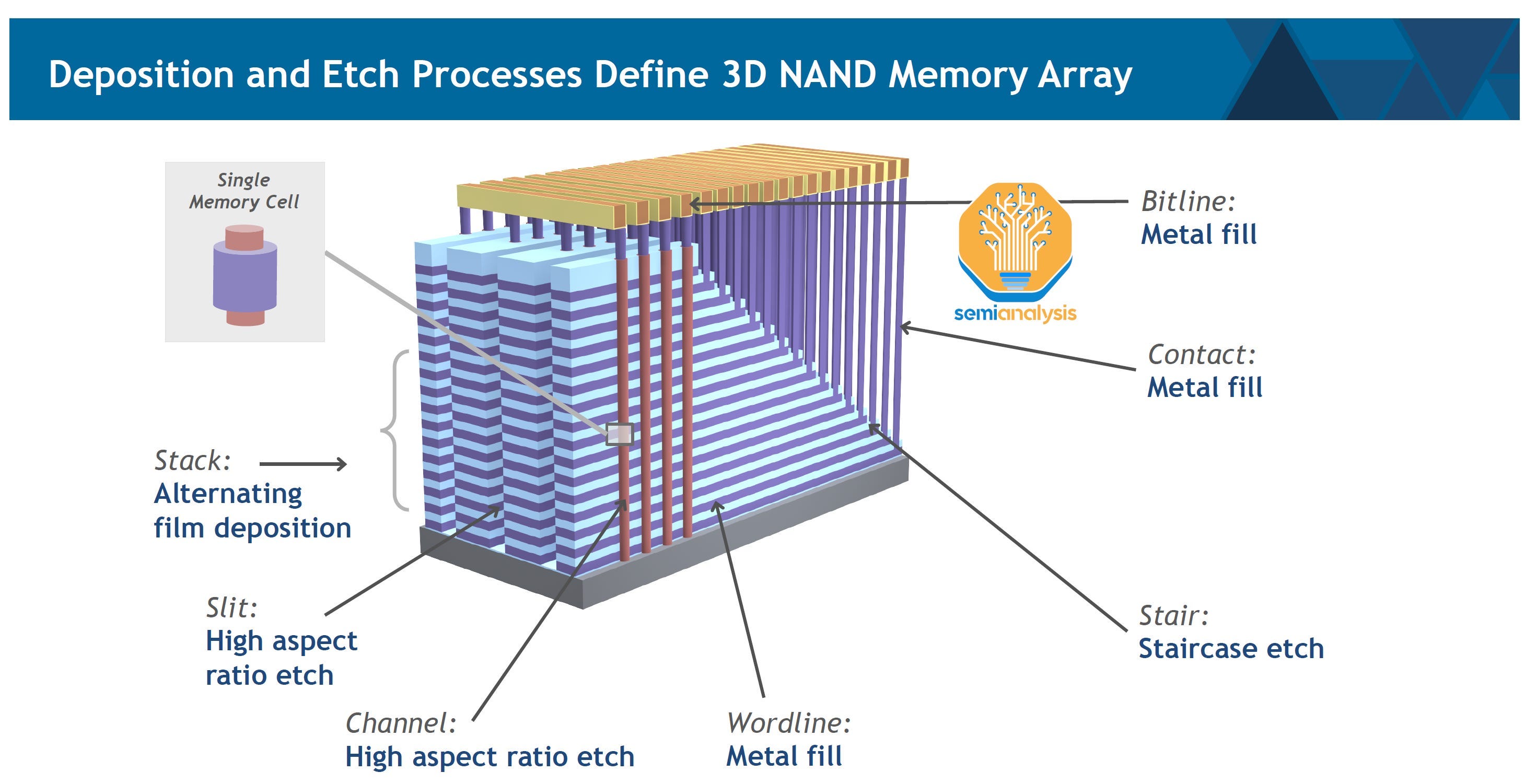
The memory cells are read and written based on charge held in a charge trap material, a layer surrounding each of the vertical channels. Charge stored there changes the threshold voltage (i.e. minimum voltage required to switch the transistor on) of the transistor. The cell can be read as 1 or 0 based on whether it switches at a given threshold voltage.
Memory producers today are primarily focused on scaling option 2, vertical scaling, because it’s the cheapest. Adding more layers means more memory cells per unit area of wafer.
Cheapest does not mean easiest. There are many, many challenges to increasing NAND layer count, and that’s why it’s interesting when one of the major companies share some of their techniques for doing so.
The major change from the 238-layer V8 generation to Hynix 321 layer V9 is an additional deck and plug. A deck is a stack of horizontal layers, alternating conductive and insulating layers, that is processed all at once. The layers are deposited, patterning and partial etch of the contacts is done (a contact is needed at each conductive layer to access the transistors gated by that layer – this is the wordline of the memory), and the channel holes are etched and filled with polysilicon and the charge trap layer surrounding it. The “plug” term you see in the images denotes this completed, filled channel that plugs the hole.
This is the process for completing a single deck. More decks can be made by repeating the entire cycle again, atop the existing deck. This is difficult too since the decks need excellent alignment to each other – the new plugs must be built directly over existing – as the wafer starts to warp and bend as stresses build up from hundreds of imperfect layers deposited atop each other.
Most of the Hynix paper here was concerned with better connecting decks and dealing with nearly 100 additional layers. They claim to be using low stress materials, improved overlay control, and “locally forced” control (possibly a backside stress control film).
Etch and other processing steps become increasingly difficult as you try to do more layers in one deck. The limit for Hynix appears to be about 120 layers. The channel etch is difficult to yield a straight, uniform cylinder with an aspect ratio ~1:100. This requires the high aspect ratio etch tools, now using cryo etch, that Lam traditionally dominated but TEL is encroaching on. It’s one of the most important and difficult to produce tools used in NAND production.
When the number of layers per deck can’t be increased, the number of decks must be increased instead. This adds a lot of processing steps. From V8 to V9, Hynix says there are 30% more process steps overall and 20% more etch steps. Don’t get too excited, WFE bulls, the layer increase was close to 35%, so layer count is increasing faster than processing steps.
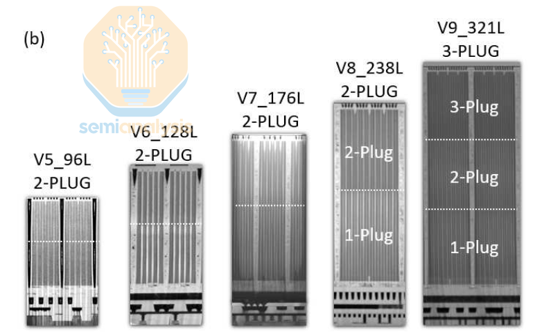
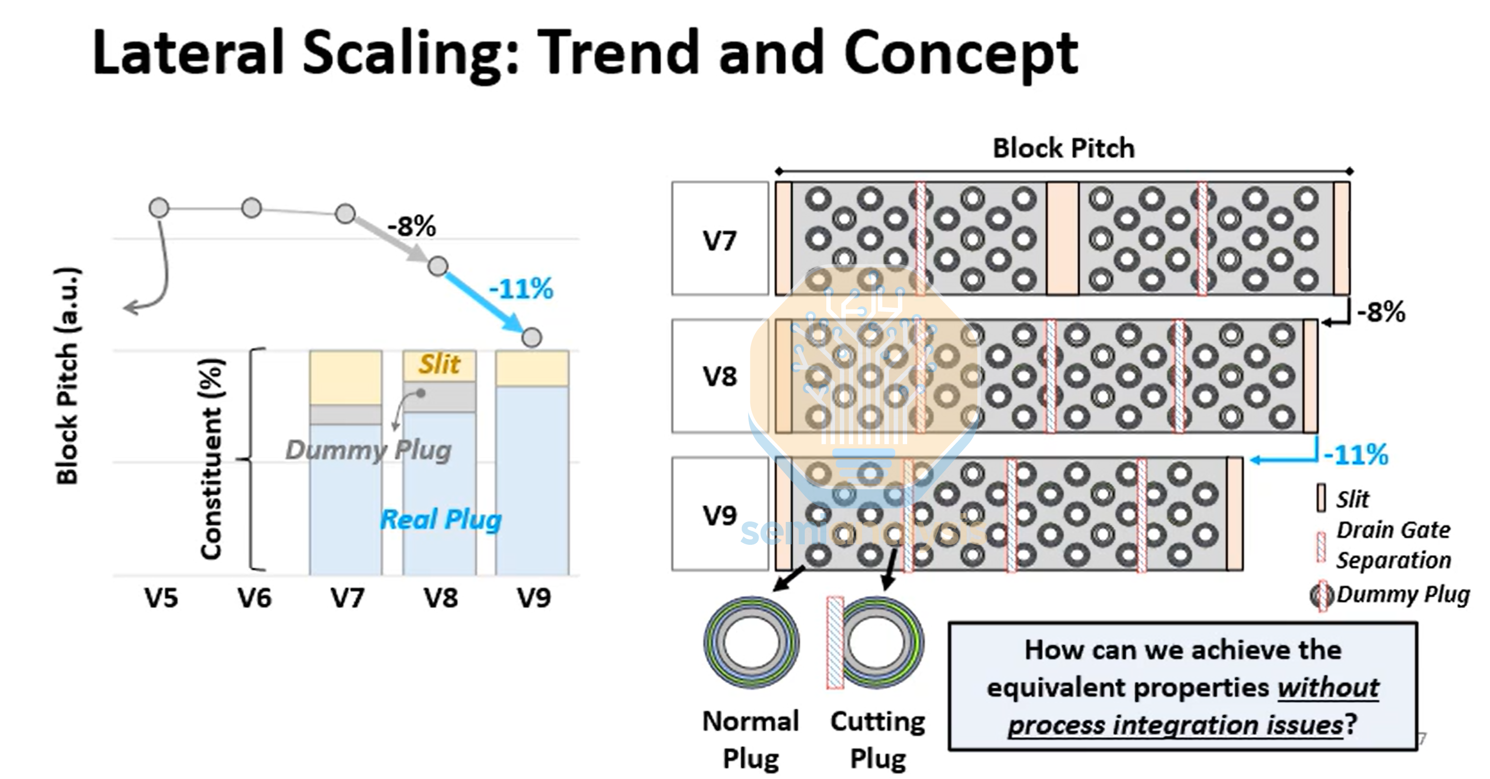
While the technology is interesting, the commercial position of Hynix’s 321L V9 product isn’t great. Its 21 Gb/mm2 is comparable to Micron 276L G9, but Micron achieves that density with only 2 decks, which will be substantially lower cost. Meanwhile Sandisk/Kioxia’s upcoming 332L BiCS10 with 3 decks will be far denser, 29 Gb/mm2 for TLC (detailed explanation below of what TLC means) and QLC demonstrated at >37 Gb/mm2. Still, the WFE intensity increase and methods for producing 3-deck stacks should be generally similar across SK Hynix, Micron, and Samsung. Note that Samsung is skipping 3xx layers altogether, going from 286L 2-deck in V9 to 43x layers, 3 decks in V10.
3D NAND: Samsung Molybdenum
At IEDM, Samsung presented an improvement to their existing V9, 286 layer technology. From V5 on, they’ve used tungsten (W) as the wordline metal, in other words the gate metal in the memory bit cell. Here, they showed a serious performance improvement by switching to molybdenum (Mo).
Mo is more difficult in pretty much every way – chemically, mechanically, electrically – versus manufacturing with W. The ALD chemistry is not as mature for Mo, and it readily oxidizes, which degrades performance. Deposited Mo tends to have greater stress variability, due in part to less mature ALD processes, which make it more likely to warp or even crack wafers.
The benefits are worth the trouble: Samsung claims contact resistance is reduced by 40% with Mo, which is crucial when trying to read an already small current that must flow through 300+ cells in series, each with its own contact resistance. Read time is improved by more than 30%, and failure rate in lifetime testing reduced by 94%.
They haven’t detailed every challenge in the Mo integration and how it was solved, but they do note the ALD chemistry, which is interesting. They do not directly deposit molybdenum, instead growing a seed layer of MoN which is then converted to pure Mo. Atop a pure Mo seed layer, thicker bulk material can be grown, resulting in a linerless, high quality Mo layer. Liners are traditionally needed to prevent metals from migrating and degrading over time, but they are not conductive and take up real estate. A linerless process can enable both better performance and further shrink in future nodes as well.
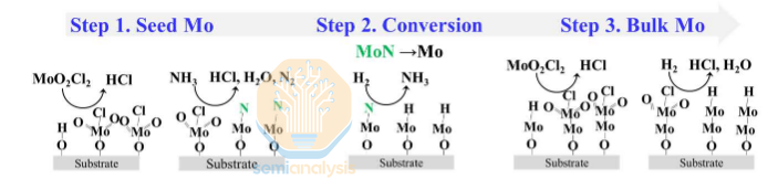
Lam is dominating Mo deposition tools, taking share from AMAT W tools and beating out TEL and others.
Layer scaling is the easiest and most cost-effective way to scale 3D NAND at the moment, but chipmakers are still pursuing the other methods listed above. The most exciting paper in the NAND track was on one of these other methods: SK Hynix showed a new method for logical scaling.
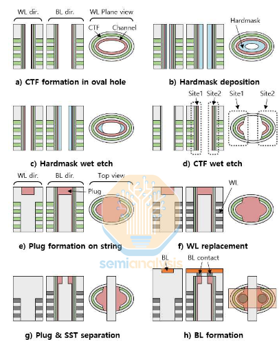
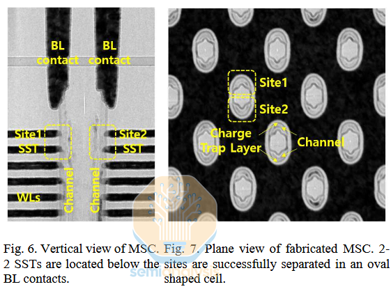
3D NAND: SK Hynix Multi-Site Cell / 5 Bits-Per-Cell
Above we talked about NAND bit cells encoding information via the threshold voltage of the cell access transistor. Different threshold voltages correspond to different states of the memory cell, and the threshold voltage is determined by a charge stored in a charge trap layer around the transistor channel. If your cell has 2 distinct threshold voltages, it can store 1 bit of information, since it can be read as either on or off. Encoding 2 bits requires capability for 4 distinct threshold voltages, 3 bits need 8 threshold voltages, and so on. The common nomenclature is SLC (single-level cell) for 1 bit per cell, MLC (multi-level cell) for 2 bits per cell, TLC (triple-level cell) for 3, and QLC (quad-level cell) for 4.
The benefit here is storing more bits in a cell directly increases overall memory capacity without increasing chip area or number of layers. QLC is common today, but there isn’t even a common abbreviation for 5 bits per cell, let alone anyone producing it.
Except, now, SK Hynix. They showed a clever architecture for producing a 5 bits per cell NAND. The key concept is dividing the channel in to 2 half-cylinder “sites”. Each site can then act as an independent channel, effectively doubling the number of channels. These half-cylinder channels aren’t as performant as larger, full cylinders, so the number of memory cells doesn’t outright double. But storing 5 bits per cell becomes much easier.
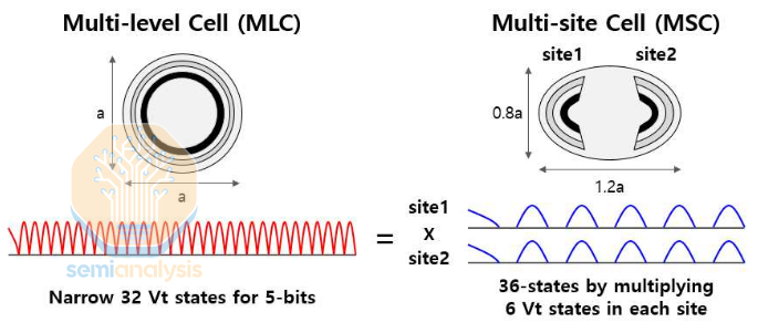
In a traditional architecture, each channel would need to store 32 distinct threshold voltage (Vt) levels to enable 5bpc storage. If you imagine the threshold voltage range to be 1V in total, each Vt step is now just 1/32 of a volt. In this multi-site architecture, reading just 6 distinct Vts from each site is enough to get you 36 distinct states (enough for 5bpc plus a few unused extras) by reading a set of 2 sites in tandem. And remember 2 sites fit in roughly the same area as 1 traditional channel, so the end result is 36 easy to read Vt states rather than 32 very difficult ones.
There’s a catch, of course: this is difficult (i.e. expensive) to manufacture. Etching the high-aspect ratio channel and depositing multiple high-quality films into it is already one of the key challenges in 3D NAND. This multi-site process requires dividing each of those holes precisely in 2, depositing a wall between, then depositing the traditional materials in an odd, asymmetric new shape. Hynix has demonstrated its possible in an R&D setting, but it’s unlikely this technique is cost effective for now.

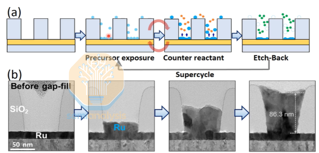
Next Gen Interconnects: Samsung Ruthenium
As semiconductor nodes scale below 10 nm, traditional copper (Cu) interconnects encounter a critical bottleneck caused by the “size effect,” where resistivity rises sharply as the relative volume of barriers and liners increases. To address this challenge, the industry has begun exploring ruthenium (Ru) as a superior alternative.
Samsung introduced Grain Orientation Engineering through Ruthenium Atomic Layer Deposition (ALD), achieving a highly textured film with 99% (001) orientation. Compared with traditional sputtering (PVD) or conventional ALD processes, this approach significantly reduces electron scattering at grain boundaries. Experimental results indicate that in ultra-fine interconnects with a cross-sectional area of only 300 nm², ruthenium lines fabricated using orientation engineering exhibit 46% lower resistance. Also, TCAD simulations on Gate-All-Around (GAA) FET structures showed a 26% RC reduction when using highly textured Ru M1 lines.
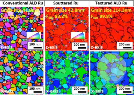
Through precisely engineered “super-cycle” steps, ozone etch-back is utilized to remove unnecessary nuclei from the sidewalls, achieving perfect bottom-up filling. More importantly, the deposited Ruthenium undergoes recrystallization after heat treatment, merging into a near-single-crystal structure. This aligns the vertical current flow perfectly parallel to the low-resistance c-axis, thereby maximizing the device’s conductive performance.
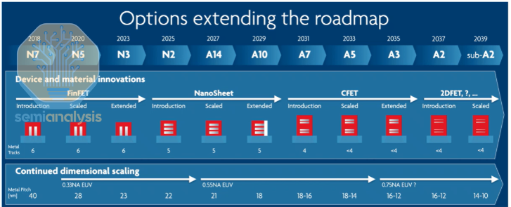
Next Gen Interconnects: IMEC 16nm Ru Metals
According to Imec’s published roadmap, there are two critical inflection points:
A14 to A10 nodes: This marks the transition from copper to Ruthenium, at least starting from the M0 layer, because ruthenium exhibits lower resistivity sensitivity than copper at extremely fine dimensions.
A7 node: This is where 18 nm or 16 nm pitches are introduced. Once we reach 16 nm pitch, it may represent the practical limit achievable with single-exposure, high-numerical-aperture (High-NA) EUV lithography.
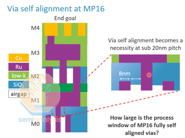
Why Fully Self-Aligned Vias?
At a 16 nm pitch, the via critical dimension (CD) is approximately 8 nm, with an 8 nm spacing as well. Such extremely small dimensions introduce significant challenges:
Air Gap Protection: To optimize RC delay, ruthenium interconnects typically require air-gap structures. If the via opening is too large, it may inadvertently breach the underlying air gap, leading to failure.
Reliability: Self-alignment can significantly improve TDDB (Time-Dependent Dielectric Breakdown) lifetime.
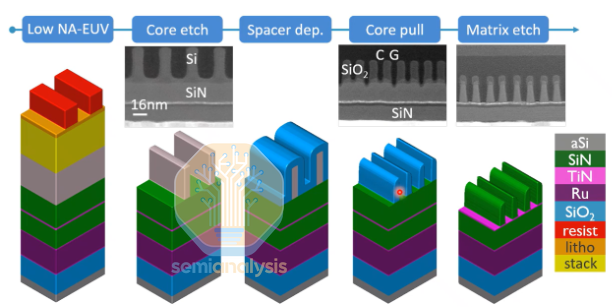
The overall process is as follows:
First use low-NA EUV lithography for patterning the stacked layers and photoresist. Next, the patterns are transferred to the silicon layer through a combination of dry and wet etching. Spacer deposition and etch-back are then applied to achieve double patterning. After that, CMP (Chemical Mechanical Planarization) is performed for surface flattening, and finally, selective removal of SiN is carried out.
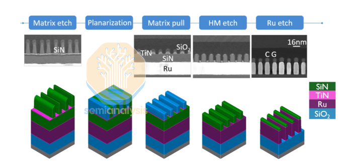
Two-Layer Metal Process:
M1 Formation: After ruthenium etching, oxide is filled and planarized by CMP, stopping selectively on the SiN layer.
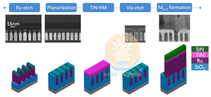
Via Opening: Deposit a 5 nm TiN hard mask, perform lithography, then etch TiN first, followed by selective etching of SiN to make a via etch
Self-Alignment: Combine mild oxidation and wet cleaning to remove the trench bottom, creating a perfectly self-aligned via. Subsequently, deposit approximately 15 nm of CVD Ru and proceed with M2 patterning.
2D Materials
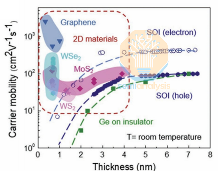
2D transition metal dichalcogenides (TMDs) keep resurfacing in logic discussions for the same reason silicon keeps getting punished as gate lengths push into the sub-10 nm regime. Once channels and electrostatics are forced into ultra-thin geometries, off-state leakage stops being a design nuisance and starts becoming a physics wall, driven by direct source-to-drain tunneling. TMDs remain one of the few plausible levers to keep leakage under control because the combination of a larger bandgap and higher effective mass suppresses tunneling. That matters precisely where conventional silicon FETs begin to leak badly at very short gate lengths.
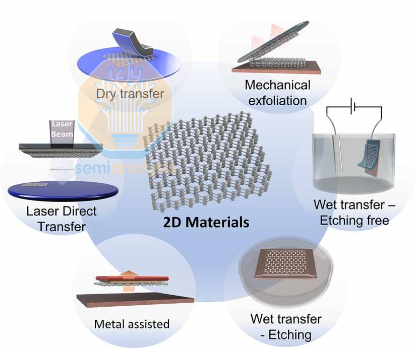
The catch is that this is no longer a monolayer physics story. It is a manufacturing story. The first gating factor is high-volume manufacturing: no matter how elegant the device architecture looks on paper, the industry only gets paid when it can repeat the same outcome across a 300 mm line. Many synthesis conditions used to achieve high-quality 2D films come with steep integration penalties, including growth temperatures that can exceed ~800 °C, plus broader environmental and safety concerns tied to precursors and chemistries. That is why the practical near-term path has increasingly emphasized transfer-based integration at relatively low temperatures, with IMEC’s 300 mm-compatible dry transfer highlighted this year as a way to mitigate void formation and improve post-transfer uniformity. At the same time, transfer remains hard to scale for real semiconductor manufacturing. Direct growth on 300 mm target wafers is still the long-term target, not an optional nice-to-have.
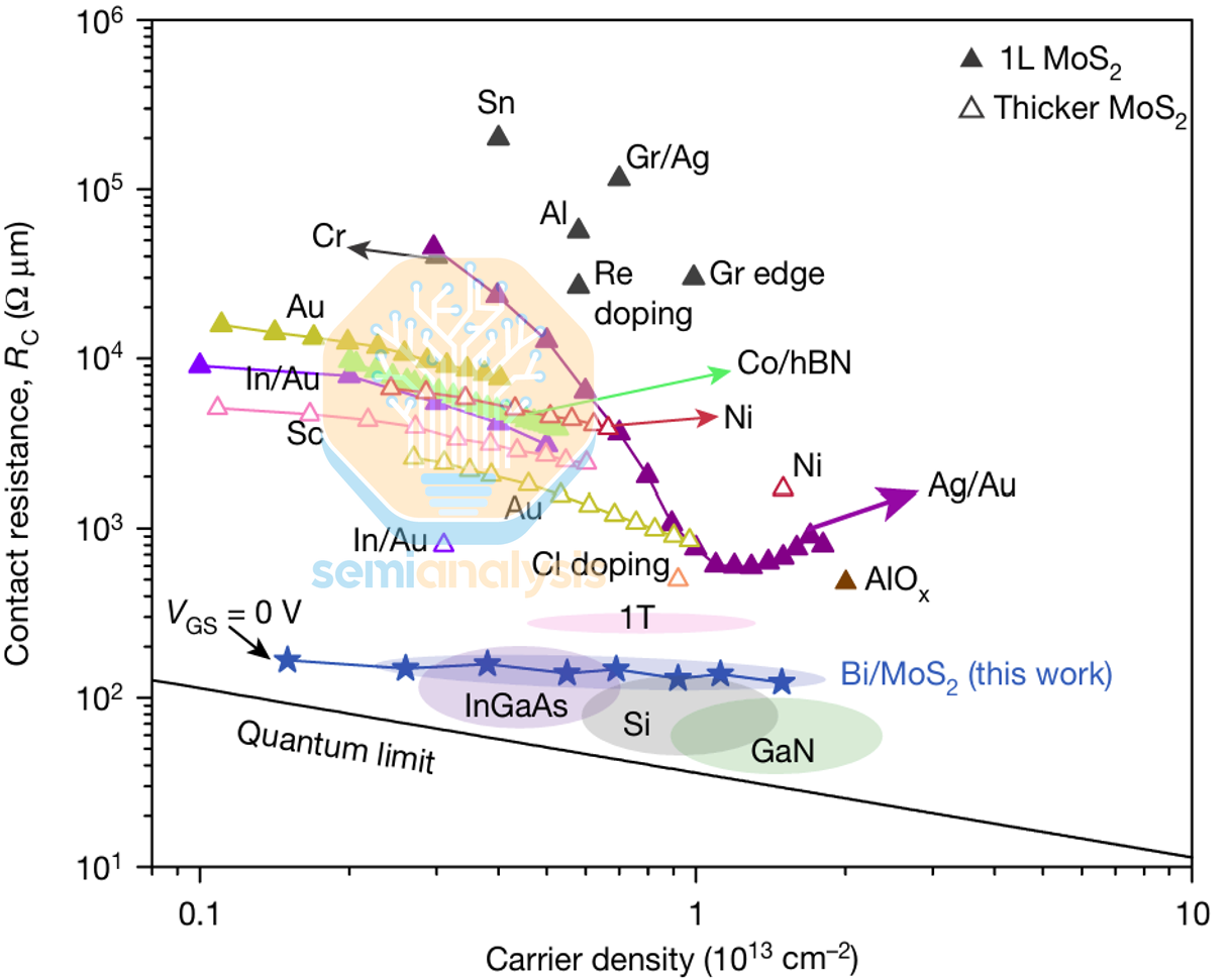
Once you accept that the near-term battle is integration, the next battle is even more unforgiving: contacts. Performance must improve to meet industrial requirements, and contact resistance has always been the focal point because it determines whether the device is contact-limited. Plenty of prior work reports low n-type contact resistance for MoS₂ under specific contact schemes, but the fine print is that these results are often demonstrated at high VGS and VDS, which is not the bias regime that matters for products. The relevant target regime is low voltage operation, with |VGS| < 1 V, |VDS| < 0.1 V, and contact resistance Rc < 100 Ω·µm. That reframes the goal: you need high carrier concentration at low bias so Rc can move toward the quantum limit under realistic operating conditions, not just under overdrive.
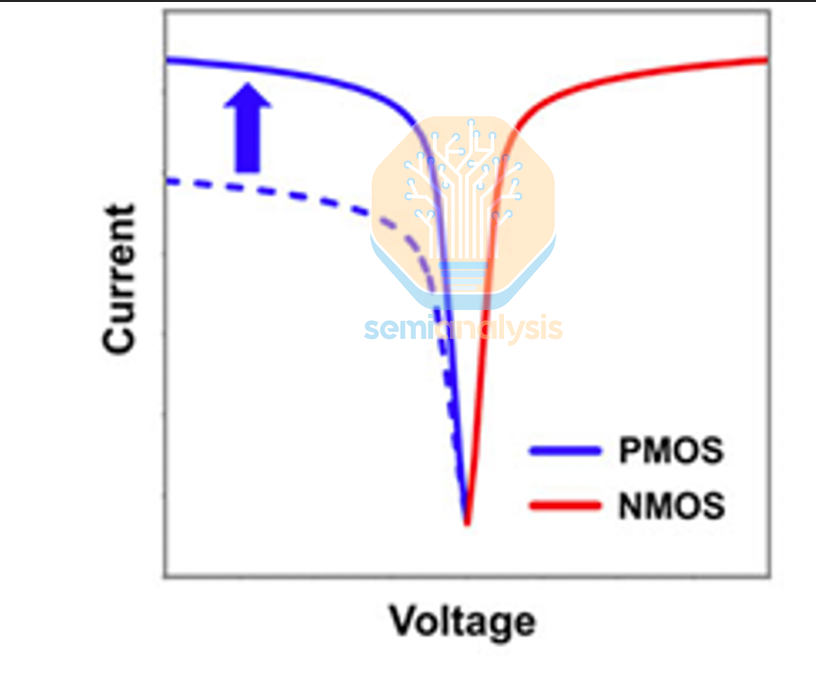
CMOS viability then runs into the familiar asymmetry problem. P-type TMD FET performance remains inadequate and is generally inferior to n-type counterparts, and the gap looks tied more to processing defects and interface physics than to a simple lack of effort. In practice, p-type behavior can drift toward n-type due to defects introduced during processing, which degrades hole injection and drives p-type Rc upward. Prior studies repeatedly point to Fermi-level pinning as a core mechanism, where pinning tends to anchor the Fermi level closer to the conduction band edge than the valence band edge. That increases the effective p-type Schottky barrier height and impedes hole injection. Other work highlights interface dipoles at the metal-TMD interface as another source of unwanted potential shifts that further suppress p-type injection. The implication is straightforward: high p-type Rc is still a first-order bottleneck, and p-type engineering has to catch up before “CMOS with TMDs” can be more than a slogan.
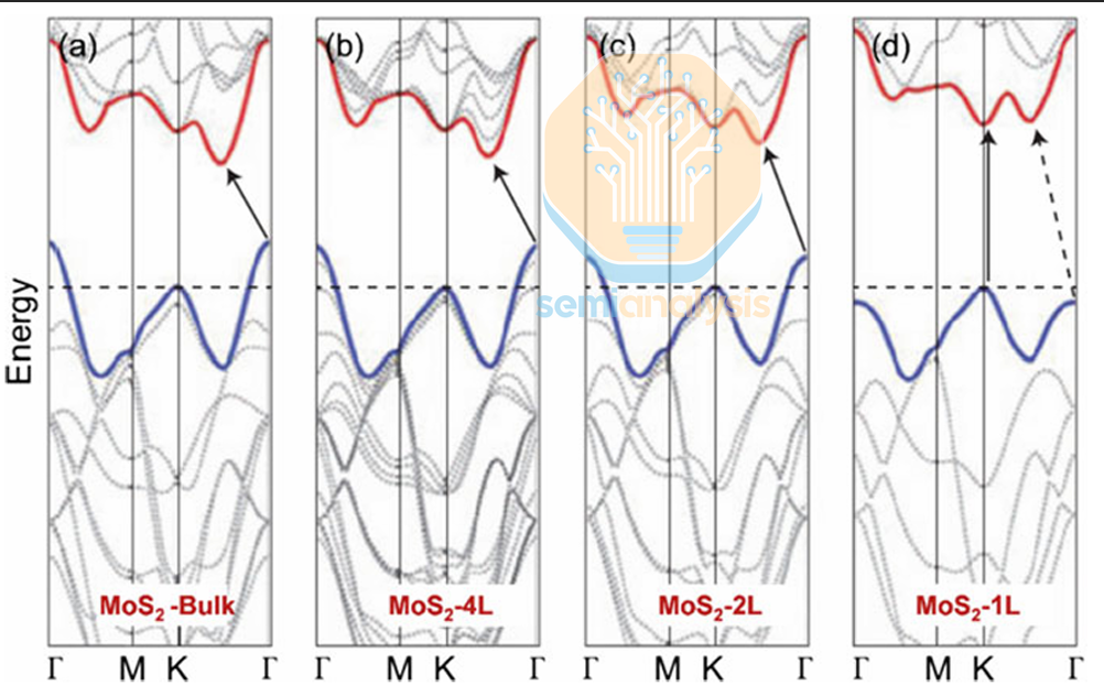
Even if you solve contacts and polarity symmetry, the next constraint is not a heroic single-device metric. It is variability, driven by film quality and layer control. Transfer-related and manufacturing-related damage remains visible: low transfer yield and structural damage such as stacking faults, vacancies, and other crystallographic imperfections are frequently introduced during processing. Layer count adds another variability axis. As the number of layers increases, the bandgap generally narrows and often transitions from direct (monolayer) to indirect (multilayer), which changes electrical characteristics materially. Multilayers can be more mechanically robust during fabrication, and multiple transport paths can reduce the apparent sensitivity to localized defects. That is why multilayers can look like a pragmatic engineering compromise. The catch is that controlling bi-layer, tri-layer, or thicker TMD growth is still difficult, often producing mixed monolayer/multilayer regions and stacking sequence errors that widen device distributions even when the average device looks fine.
The scaling argument that keeps TMDs on the table is being framed more explicitly this year in the context of gate-all-around (GAA) nanosheet transistors. Shrinking physical gate length below ~10 nm effectively forces channel thickness to well under ~5 nm if you want to sustain subthreshold swing below ~70 mV/dec. If you cannot hold subthreshold swing down, you either accept excessive off-state leakage or you raise operating voltage. This is the silicon problem in its most concrete form: at sub-10 nm, conventional Si FETs see off-state leakage rise sharply because source-to-drain tunneling ramps. TMDs are positioned as a way to blunt that tunneling through bandgap and effective mass, keeping off-state current lower in the same geometry.
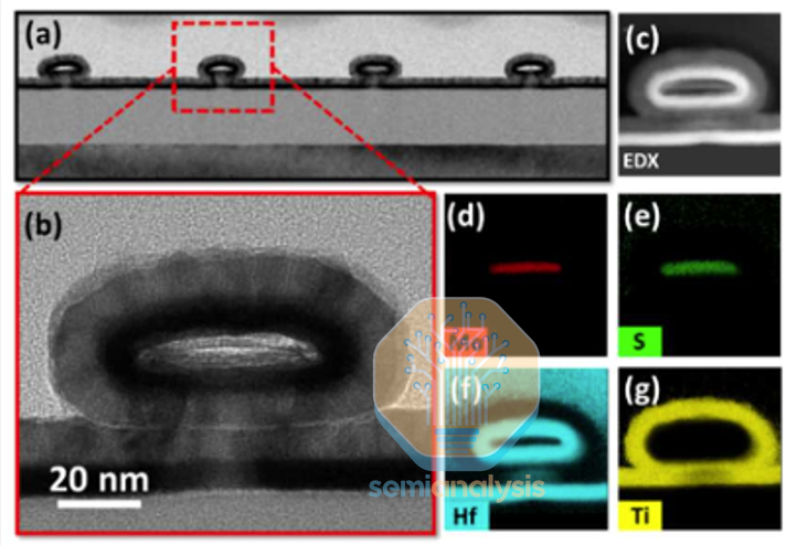
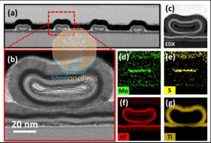
Threshold control and doping then become the next translation barrier because the silicon toolbox does not port cleanly. There is still no practical, reliable substitutional doping technique for TMDs at the level the logic industry would call “manufacturable,” likely due to poor dopant incorporation and stability. Ion implantation, the workhorse in silicon, can severely damage 2D materials and introduce defects that degrade mobility and device lifetime. In that environment, many studies lean harder on work-function engineering and interface physics: careful selection of contact metals for both n-type and p-type devices, Vt tuning via Fermi-level depinning at the metal-TMD interface, and charge transfer effects from gate dielectrics rather than classical doping. One of the clearer architectural intent signals in this direction was the 2022 TSMC report of a GAA monolayer MoS₂ n-type FET, positioned as evidence that the TMD nanosheet concept can be made real, at least on the n-type side. In TSMC’s 2025 IEDM study on 2D FETs, the key lever for improving p-type performance is inserting an interlayer (IL) between the 2D channel and the high-k gate dielectric to reduce the screening and remote-phonon-scattering penalties that otherwise drag mobility and stability. They frame the results around EOT scaling and IL selection: shrinking EOT from ~2 nm to ~1 nm at a constant overdrive (Vov = 0.7 V) tightens electrostatics, delivering a ~2–3× increase in ON-current (ION) and cutting hysteresis by roughly 30–40%. The subthreshold swing (S.S.) improvement, however, is only marginal, still far from the silicon ~60 mV/dec benchmark, with 2D devices remaining around the ~1xx mV/dec range, implying the remaining limitation is not just gate control but also the capping stack and the 2D channel/interface quality itself. On IL chemistry, O-based IL options degrade ION, which they attribute mainly to worsened S.S. from higher surface roughness introduced during fabrication, pushing them toward N-based IL for the main optimization path; with added surface pre-treatments to suppress defect-driven degradation, both S.S. and hysteresis continue to improve monotonically as treatment intensity increases. The endpoint signal is that hole mobility can exceed 100 cm²/V·s in monolayer WSe₂, positioning IL engineering plus disciplined surface processing as a credible route to closing the p-type gap.
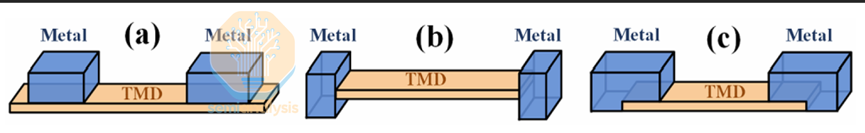
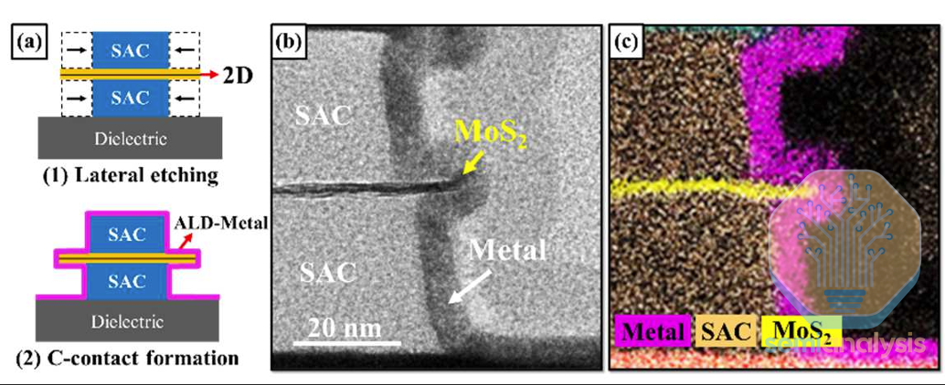
At that point, even the geometry of the contact stops being a secondary detail because it governs whether a “good contact” concept can be built repeatedly at scale. The optimal contact geometry remains under debate, and purely top-contacted or purely edge-contacted configurations can be difficult to realize robustly in production. Some work proposes C-contact, hybrid, or combined topologies as a manufacturable path, with first-principles calculations suggesting enhanced performance for C-contact-like configurations (including non-van-der-Waals sandwich contacts). The direction of travel is clear: the industry is converging on manufacturability-driven compromises where the theoretical ideal matters less than the geometry that survives process variation and still delivers acceptable Rc.
Finally, the pace of 2D TMD development is gated by physical modeling maturity, which is one of the least glamorous but most determinative constraints if 2D devices are ever going to move from lab cycles to product cycles. More realistic, predictive simulations with low computational cost are needed. Two main approaches dominate today: TCAD-based device simulation and first-principles calculations. TCAD is routine for silicon, but dedicated TCAD models for 2D devices will become essential, and today they are still constrained by the lack of well-defined, physically grounded parameters for TMD physical, chemical, and transport properties. First-principles methods (including DFT) remain invaluable for mechanism understanding, but computational cost and atomistic system size limits restrict how far they can be pushed toward realistic devices and variability studies. Efficient, physics-based toolchains that bridge these worlds are not optional infrastructure, they are a prerequisite for faster iteration.
Taken together, the 2D FET results highlighted this year read less like a celebration of a new material and more like a checklist of what has to become boringly repeatable before 2D logic can matter. Wafer-scale integration pathways and the hard limits of transfer scaling. Low-bias contact resistance targets that look like product constraints rather than lab bias points. P-type performance as a first-order bottleneck driven by pinning and interface effects, not a minor lag. Layer control and defect damage as variability problems that will dominate distributions even when headline curves look impressive. Even as the scaling narrative stays anchored in stacked GAA nanosheets and tunneling suppression, the same studies implicitly concede that Vt control and doping are immature and will require interface- and dielectric-based strategies. Contact geometry pragmatics and modeling toolchains are the enabling infrastructure for future credible progress.The next meaningful milestone is not another record transfer curve. It is a wafer-scale, low-bias, statistically credible demonstration where integration, contacts, polarity symmetry, and variability all move together in the right direction.
Next, we’ll cover the most important topic at the conference, the post-GAA inflection point in advanced logic: CFET. We’ll cover imec’s roadmap including when CFET will replace GAA and how many nodes it might be extended. Another imec paper detailed a clever new integration scheme to maximize both p- and n-type transistor performance in a CFET without requiring hybrid bonding. But first, the most important paper: TSMC made much further progress than anyone expected…