

Nanoimprint Lithography: Stop Saying It Will Replace EUV
NIL basics, why it won’t replace EUV, details of Canon’s tool, possible applications
Every 6 months or so, we see another round of headlines about nanoimprint lithography disrupting EUV.
It makes for good clickbait but is just not true. The technology has many interesting and valid applications, but nothing like what EUV can do. Theoretically, NIL could match or even exceed EUV capabilities. Practically, there are serious issues for NIL without any clear way forward.
We’ll explain those differences in theory versus actual in-fab practice in this report. We’ll also detail the key players in the market and the likely applications where it will work. To start, let’s cover the basics of what NIL is and what it can do:
NIL Basics & History
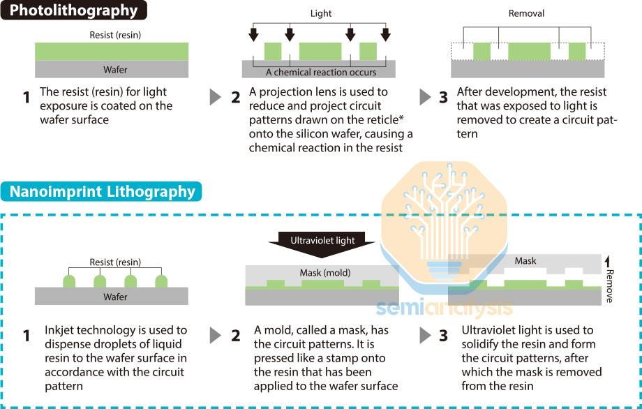
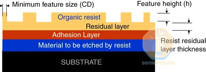
Nanoimprint lithography uses a patterned “stamp” to imprint a pattern in resin. In semiconductor production, it achieves the same end goal as photolithography à la ASML – transfer a pattern from a mask onto a wafer. These patterns are just 1 layer of the chip design. Stacking 50-100 layers, with patterning followed by other techniques like etch and deposition on each, eventually builds up a complete chip.
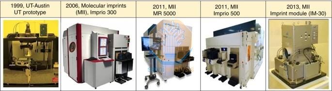
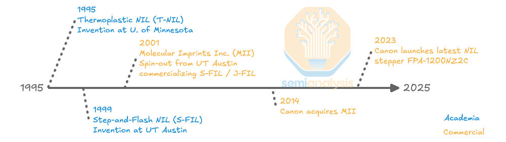
The most promising technique for nanometer-scale NIL was invented in 1996 and spun out from academia to a commercial entity in 2001 as Molecular Imprints Inc. (MII). Canon acquired MII in 2014, positioning it as their alternative at the time ASML was beginning to ship EUV into customer R&D fabs.
This is the only advanced commercial venture into NIL technology. A Chinese competitor, Prinano, recently made headlines, but is much less mature, for now. Nanonex, spun out by the inventors of NIL from the University of Minnesota, has fewer than 100 tools worldwide, mostly in academic labs. EV Group has commercial tools but explicitly aims for less advanced applications including metalenses, MEMS, and microfluidics.
Canon went all-in on NIL as its next-gen patterning tech after DUV. It’s the only thing on their roadmap beyond KrF scanners, which were state-of-the-art in 2000. As we’ll see, it was the wrong bet.
Detailed Process Flow
Canon calls its technology “J-FIL” for jet and flash and nanoimprint lithography. “Jet” refers to the method of applying resist to the wafer, followed by imprinting by the template and a “flash” of UV light to cure the resist in place.
Producing an NIL imprint starts with dispensing photoresist on the wafer. Because the resist will be displaced in 3D, rather than capturing an image on a 2D plane as in photolithography, applying it in an even layer across the entire wafer is not optimal. So traditional spin-coaters aren’t used. Instead, an extremely high quality inkjet printer deposits resist in an optimized droplet pattern. This pattern improves resist flow during patterning, reducing voids and overflow.
The resist deposition is done inside the patterning tool, to minimize queue time before patterning and wafer movement which could disturb the resist droplets. This puts resist coating in the critical path that limits wafer throughput, so speed is optimized – just one pass is needed, done in 1/3rd of a second.
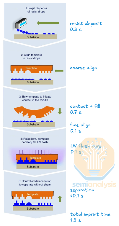
Next the mask is pressed into the resist to pattern it. A slight bow is induced in the mask so that the center touches first, then the bow relaxed as rest of the mask is lowered into contact. This pushes any excess resist outwards and ensures better repeatability and symmetry versus the entire mask contacting at once. The bow is produced by gently pressurizing the volume behind the mask with C02, causing the center to bulge out by just 10 microns, less than the width of a hair. That pressure is released in concert with the mask lowering to its final position, leaving the mask flat and in contact with the entire area to be patterned.
Once the mask is fully contacted across the entire pattern, it pauses for a fraction of a second to allow resist to flow and fill any voids, then is moved horizontally in a fine alignment step to ensure good overlay.
A UV flash cures the resin, solidifying it with the imprint of the mask. Then, in less than a tenth of a second, the mask is lifted off the patterned wafer. This completes patterning for a single exposure field. The wafer is stepped over to the next field, and the exposure cycle repeats.
Because the resin is cured during the imprint process, there is no need for a post-exposure bake as used for photolithography. This saves time and cost, but ultimately less than 1% of total wafer cycle time and cost when added up. Unfortunately, as we’ll see below, this doesn’t offset the other time and cost penalties from NIL.
Mask Process Flow
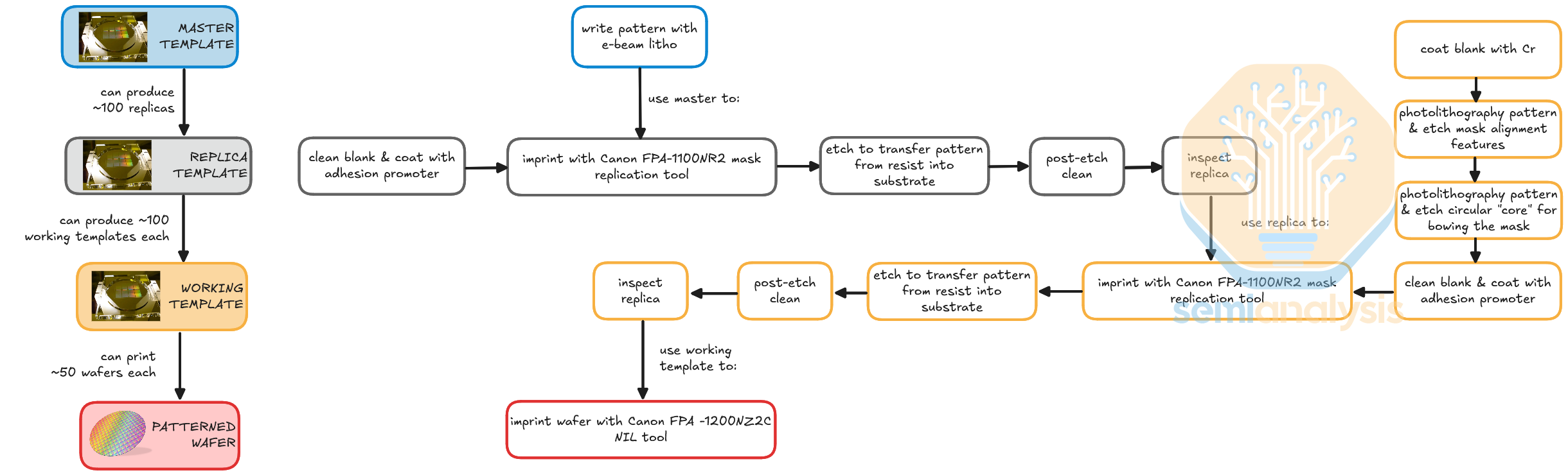
Mask or “template” production is critical to NIL performance. A defect in the template will be copied to every die it’s used to produce.
NIL masks use the same blanks as DUV optical masks, to take advantage of the existing ecosystem and economies of scale. A single exposure field of 26x33mm is patterned, with a circular region cored out to facilitate bowing during the contact process.
The first step towards producing working masks is to write a master template. Similar to a traditional DUV mask, the initial pattern is written by a multi-beam (e-beam) mask writer into e-beam resist. It is transferred into a harder material beneath the resist, probably chromium, before extra material is deposited to grow a 3D pattern.
This master template is used to make “submaster” replicas. Using a special NIL tool made specifically for template replication, an imprint is made in resist on a quartz blank. The resist pattern is transferred by etch into a chromium layer and then down into the quartz itself. This produces a 3D pattern in the quartz that matches what will be made on the wafer.
Finally, the submasters are used to produce working templates. Same as the master pattern is imprinted and etched into the submaster, the submasters are used to imprint and etch the final negative pattern into working templates. These templates can then be used to pattern wafers.
This master → submaster → working template flow is done because using an e-beam mask writer tool for every working template would be far too slow. It takes 8 hours at minimum to write a modern mask pattern.
One notable difference is that photolithography masks will be magnified by 4x by the projection optics – meaning masks can be written with features 4x larger than what will ultimately be printed. Even sub-resolution assist features (SRAFS, smaller than what the scanner can print) are still relatively large on-mask and therefore easier for the mask writer to produce.
NIL templates do not have this advantage. They must be written at the same feature size as what’s needed on the wafer. Even counting SRAFs, the most advanced photomasks today require features roughly 40nm at smallest. An NIL mask to print critical layers on advanced chips would need features closer to 20nm.
In NIL’s favor, the field area to be written is 4x smaller than what a photomask requires, since it is just equivalent to the field size to be printed. The net effect is that NIL master template writing may take less time than writing a photomask, but will need the absolute best MBMW mask writer.
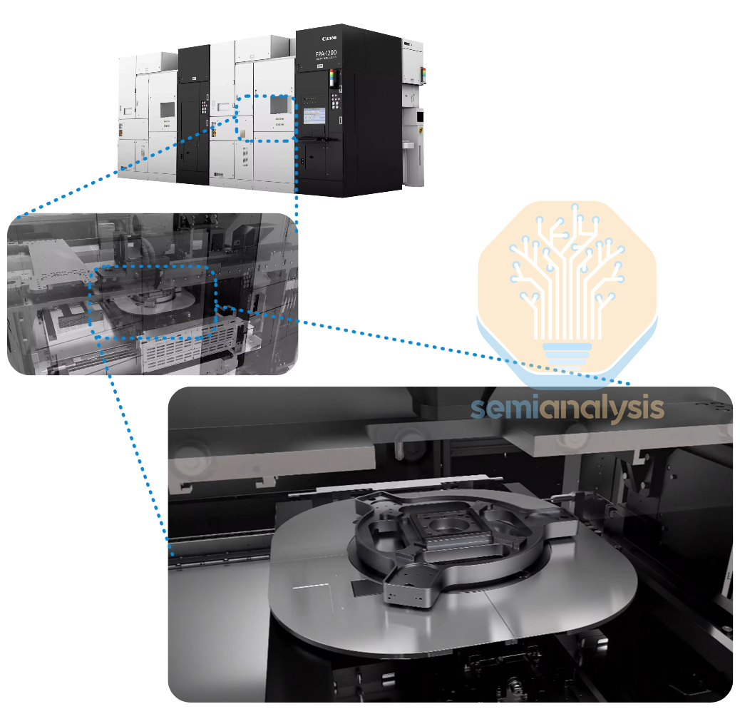
Canon NIL Tool Architecture & Capabilities
Of all existing tools, the Canon NIL machine is by far the most advanced in terms of capability and commercial readiness. Like a photolithography scanner, it has a wafer and mask motion stage. The wafer stage has coarse and fine control horizontally in X, Y, and rotation about the Z-axis while the mask stage can move up and down in Z. Both stages move with a claimed 1nm precision.
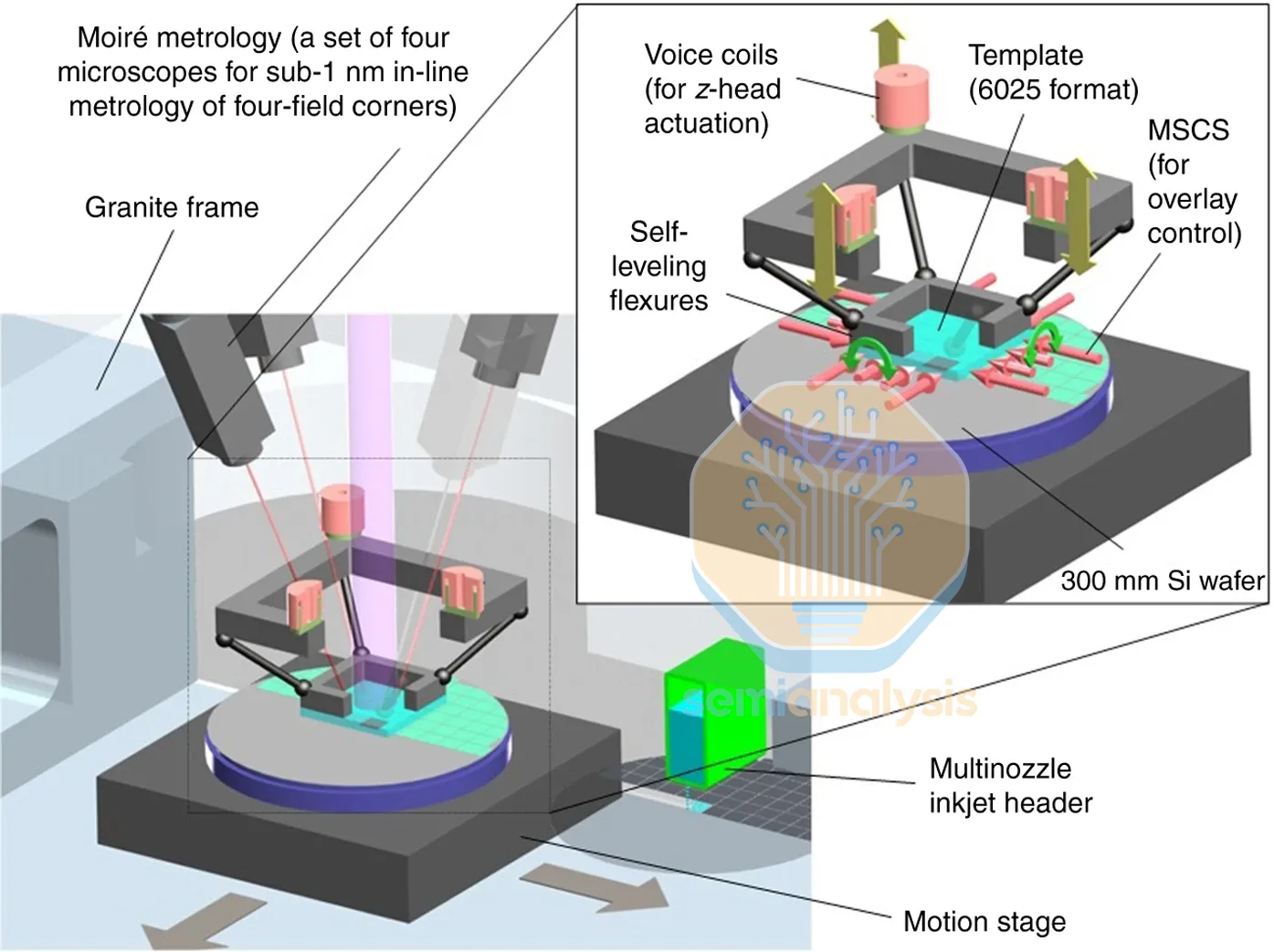
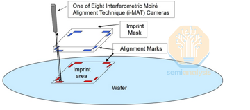
Unlike most light-based scanners, it can perform alignment metrology at the same time as the actual patterning. This is done with microscopes imaging through the clear mask to read alignment marks just outside the imaging field, enabling simple closed-loop overlay control. Canon calls this “i-MAT” for Interferometric Moiré Alignment Technique. Feedback from the alignment metrology is used by the wafer and mask stages to correct any errors as imprinting takes place.
Low-order alignment errors (for example, the mask is 5nm too far left) can be corrected by the mask stage. 16 “fingers” holding the mask each have their own piezoelectric actuator and can move independently to shift or warp the mask as needed.
High-order alignment errors (for example, complex aberration patterns caused by uneven temperature across the mask) can be corrected by selective heating of the mask with a laser steered by an array of micromirrors. At their default position, all the mirrors will reflect the laser light through the mask, heating it. When MEMS actuators behind each mirror are activated, they move the mirror to steer the light off the mask, effectively making a “pixel” that can be turned on or off to heat the mask selectively.
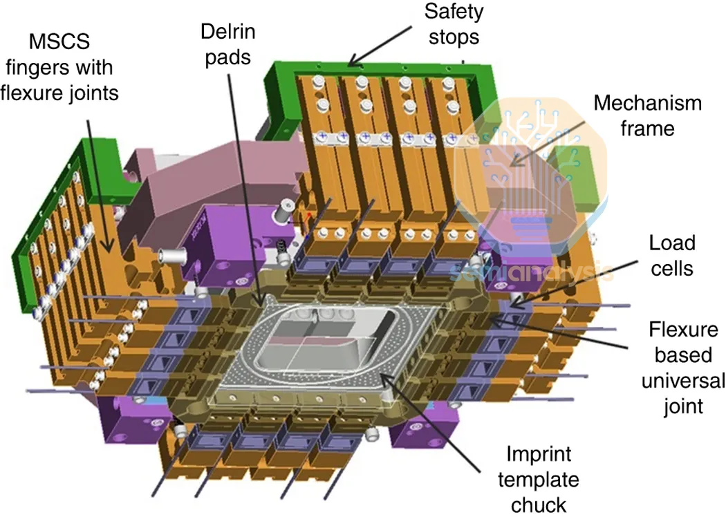
One cell of the NIL tool can process one wafer at a time. The imprint process takes about 1.3s total, along with another 10% overhead for metrology, wafer exchange, and other non-imprint tasks. This adds up to a maximum throughput of 25 wph. Canon markets them as a set of 4 cells, for a total of 100 wph.
Compare this to leading ASML photo tools which can do 330 wph for DUV and 220 wph for EUV (in practice the throughput will be lower when considering uptime, exposure dose, and other factors. We use the advertised throughput here as the practical number for NIL isn’t known).
Comparison to EUV
On paper, NIL can meet or exceed EUV resolution. Its capability is primarily limited by e-beam mask writer resolution to make the master template. This advantage would only grow at finer resolutions as stochastic errors in EUV grow exponentially near their resolution limit. E-beam master writing can mostly avoid stochastic issues by using extremely slow (high dose) resists that aren’t so sensitive to a few stray photons.
It also would be a drop-in replacement in the fab process flow. The steps that follow patterning don’t care whether the it was done by EUV or NIL.
The cost advantage for NIL tools, excluding the mask production flow which we’ll talk about shortly, is large. Most likely a 4-cell tool costs about 1/10th what an EUV scanner costs. Taking throughput differences into account the cost per wafer of NIL is still just ¼ that of EUV, again counting just the patterning tool.
Power consumption is a sore spot for EUV. NIL is significantly better as it does not need a source with the power-hungry CO2 drive laser. Canon claims 90% lower, which would put them at ~100 kW versus >1 MW per EUV tool.
Added up: great resolution, no stochastics issues, cheaper to run – why wouldn’t chipmakers be rushing to replace their EUV tools with NIL?
Key Challenges
It turns out NIL in practice is very different from NIL in theory. We’ll take the key challenges one at a time:
Mask Lifetime
The key issue is that nanometer-scale 3D structures are fragile. Imagine you had a stamp with features as small as a human hair. Just breathing in its direction might ruin it…
Now imagine a stamp with features 4 orders of magnitude smaller, so 10,000 of them lined up are the width of a hair. Now use that to stamp a wafer once every second. And remember, any defect or broken part on that stamp pattern means every chip it prints may be defective.
How long does that stamp last? Right now, about 50 wafers.
Canon claims more than 10x that number, but customers demoing the tool say otherwise. Compare that to a photolithography mask which has a lifetime of well over 100,000 wafers. It creates a massive problem with template inspection and defectivity:
Fabs have to inspect masks before they are first used, and occasionally through their lifetime. This is because any defect on the mask will be printed to every field imaged with that mask. An undiscovered “repeater defect” like this can easily run up millions of dollars in scrap wafers.
The traditional solution is mask inspection. This is slow and expensive, but the economics make sense for a photomask which costs $100k - $1M+ and will support months of production.
But inspecting every template is just not feasible when the inspection time is about the same as the lifetime of the mask in production. Fabs would need 4 mask inspection tools for each 4-tool NIL cell. Equipping a single modern fab this way would consume roughly the entire annual output of mask inspection tools worldwide.
The practical way forward is presumably to inspect the master template and selectively review a small number of replicas and working templates. Finding the correct inspection intensity for replicas can only be done through experiment with many masks, inspections, and wafers – in other words it will be expensive and require months or years of work.
Fundamentally this goes back to the challenge of making nanometer-scale mask features hold up to the stress of repeated “stamping” of wafers. Pattern features tend to break off, creating both a defect in the mask pattern and a loose particle. It’s not clear that there is any solution to this problem or roadmap to get there. Without it, NIL will never compete with EUV.
Beyond mask inspection and defectivity, there are some lesser (but difficult!) challenges that at least seem solvable:
Overlay
Overlay, the alignment of the pattern being printed to other layers already on the wafer, is about 4x too large right now. This is far from trivial but ASML has proven it’s possible for optical systems at least.
One of the key methods of measuring and controlling overlay is through alignment marks. These are small designs printed in between the actual chip designs, an area that will be cut away when the completed wafer is diced into chips. These marks can be read to determine where existing layers on the wafer are placed, and to calculate imperfections in the wafer. These calculations enable feed forward control that deforms the mask, as discussed above.
Generally it is better to read as many alignment marks as possible. This is especially important for high-order corrections (complex deformation shapes) that are necessary to achieve nanometer-level overlay error.
ASML’s “Twinscan” architecture enables reading many marks over the entire wafer surface, because 1 wafer stage can do metrology while the 2nd does actual exposures. Canon’s NIL architecture has a single stage, so it must either do very little metrology or do it at the same time as exposure to maintain good throughput.
Through-mask metrology for NIL is an innovative solution, but may be limited in its current form. For each printing field, it can only read metrology marks at the corners of the field. Compare this to ASML’s tools which read 10x more marks over the entire wafer, and are therefore much more capable of correcting overlay errors.
This is fixable for NIL but may need major changes to the tool architecture.
Alignment mark size
Each tool vendor traditionally has its own alignment marker designs (ASML’s old logo was an alignment mark). Canon’s design for NIL right now is too large, so it wastes expensive wafer area. Technically a smaller alignment mark should be feasible, but possibly Canon is limited by IP or other constraints.
Mask pattern roughness
Line roughness in the design written to the mask can lead to defects or poor performance of the resulting chip. For example, a rough line that defines a wire could mean the wire shorts out by touching its neighbor. This issue is due to the “patterning stack” being immature – the various chemical layers that are used to print the pattern and transfer it to lower layers in the wafer. For photolithography, this is still a challenging area at the leading edge, but is mature as a field and can build from decades of experience.
Customer Feedback
Customer behavior is a good indicator of where the technology actually stands. Kioxia and Micron both are demoing the tool either in their R&D fab or by running wafers with Canon. Keep in mind these potential customers have every incentive for NIL to work: it’s a (theoretically) cheaper alternative to EUV and even advanced DUV tools. Unfortunately, the results are not good.
Both give similar presentations at SPIE, repeating the same complaints each time. A sampling from the last 2 years:
“Defects are the biggest weakness for nanoimprint”
“High number of defects in nanoimprinting”
“Challenges: template cost and lifetime”
They even suggest the mask roughness issue, stemming from printing small features on the master template via e-beam, necessitates pitch splitting (SADP) for features below 20nm. In other words they see a practical limit on NIL resolution.
The conclusion by the customers is very clear: NIL is not ready for prime-time in advanced chips. Progress year-on-year does not suggest it is on track to change that.
Export Controls
Note that the overlay capability, <4nm, and theoretical resolution of well under 45nm mean the tool is restricted by U.S. export controls. Japan doesn’t publish exact numbers but likely also restricts this system.
But, as we discussed in our recent report on Huawei Ascend production, the Japanese export controls do not prohibit re-export. This is a serious gap. A Canon NIL tool sold through Japan could be re-exported to any Chinese leading fab. Theoretically, this allows EUV-level technology into China.
https://newsletter.semianalysis.com/i/174558658/export-control-lag-benefits-smic
As we outlined above, the practical capabilities of the NIL tool do not match EUV. The advertised overlay spec of NIL is not good enough for critical layers of advanced chips. And defectivity would make the economics challenging if not impossible. But, without any good alternatives, it might make sense for SMIC or a Huawei entity to give it a try.
In short, this is yet another example of why the export control carveouts for Japan and the Netherlands should be eliminated. Their export control regimes, especially Japan, are not keeping up.
Where can NIL succeed?
The good news is, there are a few potential applications where NIL might succeed and are well on the way to being used: