

Scaling the Memory Wall: The Rise and Roadmap of HBM
HBM4, Custom Base Die, Shoreline Expansion, Process Flow, China Domestic Production, Samsung Qualification
The first portion of this report will explain HBM, the manufacturing process, dynamics between vendors, KVCache offload, disaggregated prefill decode, and wide / high-rank EP. The rest of the report will dive deeply into the future of HBM. We will cover the revolutionary change coming to HBM4 with custom base dies for HBM, what various different accelerators are doing with custom HBM including OpenAI, Nvidia, and AMD, the shoreline area problem, memory controller offload, repeater PHYs, LPDDR + HBM combos, and various beachfront expansion techniques. We will also discuss SRAM tags, compute under memory, supply chain implications, and Samsung.
A Brief Overview of HBM
As AI models grow in complexity, AI systems require memory with higher capacity, lower latency, higher bandwidth, and improved energy efficiency. Different forms of memory have different tradeoffs. SRAM is extremely fast but low density. DDR DRAM is high density and cheap but lacks bandwidth. The most popular memory today is on-chip HBM which strikes the balance between capacity and bandwidth.
HBM combines vertically stacked DRAM chips with ultra-wide data paths and has the optimal balance of bandwidth, density, and energy consumption for AI workloads. HBM is much more expensive to produce and has a warranted price premium to DDR5, but demand remains strong for HBM. All leading AI accelerators deployed for GenAI training and inference use HBM. The common trend across accelerator roadmaps is to scale memory capacity and bandwidth per chip by adding more stacks, higher layer counts, with faster generations of HBM. Architectures that rely on other forms of memory offer sub-optimal performance, as we have demonstrated.
In this report, we will examine HBM's present state, what’s happening in the supply chain, and the groundbreaking changes happening in the future. We’ll examine HBM’s critical role in AI accelerator architecture, the impact HBM is having on the DRAM market, and why it is upending the way memory market analysis is being performed. For subscribers, we will also address the major questions on Samsung's future viability as a supplier, as well as highlight one technological change that may reverse the trend of increasing HBM capacity.
HBM Primer
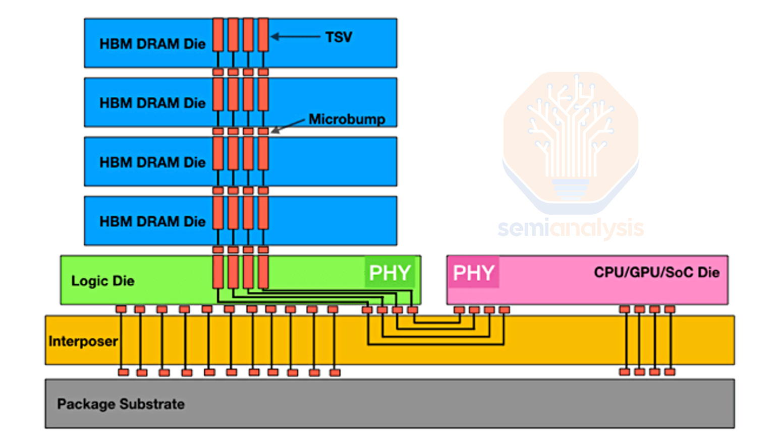
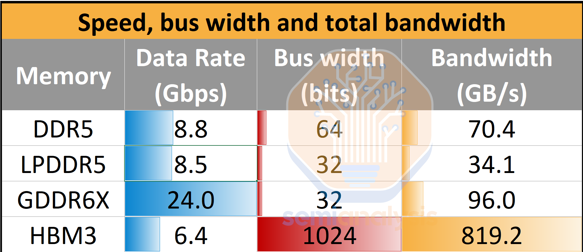
First, a brief primer on HBM - what makes it special and challenging to manufacture. While HBM is commonly associated with multiple DRAM dies stacked in a 3DIC assembly, the other key feature is HBM’s much wider data bus, improving bandwidth even with mediocre signaling speeds. This significantly wider bus results in HBM being far superior in terms of bandwidth per package than any other form of memory.
The implication of having much more I/O is increased routing density and complexity. Each I/O requires an individual wire/trace, with additional wiring required for power and control. For a HBM3E stack, there are over a 1,000 wires between the adjacent XPU and the HBM. This level of routing density is not achievable on a PCB or package substrate; therefore, an interposer (silicon or organic) in a 2.5D package assembly like CoWoS is required.
To reduce latency and energy consumption for data transfer, HBM needs to be placed directly adjacent to the shoreline of the compute engine. This makes shoreline (the edge of a SOC) more valuable as HBM can only be limited to the 2 edges of the SOC with the other 2 edges reserved for I/O off the package. This limits the area HBM can be placed in and requires vertical stacking of memory die to provide enough capacity.
To enable the 3DIC form factor, each layer of the stack needs to have TSVs (excluding the top of stack) that can deliver power and signal to the layer above. The additional area required to fit these TSVs is what makes HBM die sizes larger than their DDR equivalent: SK Hynix D1z DDR4 has a bit density of 0.296 Gb/mm2, 85% more dense than their HBM3 which is 0.16 Gb/mm2. This TSV process is one of the key differences between standard DRAM, and tooling for this is the main bottleneck when it comes to converting regular DDR DRAM wafer capacity to HBM capacity.
The other difference is at the back-end, where the HBM needs to be stacked to 9 or 13 layers in total (8/12 DRAM layers on top of a logic base die at the bottom). Along with CoWoS, HBM has brought packaging technology to the mainstream. Niche packaging technologies like MR-MUF have now become common knowledge for industry participants.
Explosive Bit Demand
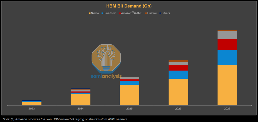
We can see the huge growth in HBM bit demand that has come alongside AI accelerator demand. Despite the rapid rise of custom ASICs, Nvidia will still command the lion’s share of HBM demand in 2027, driven by its aggressive roadmap, where Rubin Ultra alone pushes per GPU capacity to 1 TB. Broadcom follows as TPU and MTIA volumes surge, while incremental OpenAI and SoftBank projects add a smaller but noticeable lift. Amazon also emerges as one of the top HBM customers. For Amazon, it has a strategy of procuring HBM directly rather than through design partners, helping them to lower their cost. For a detailed, chip-by-chip bit forecast, refer to our Accelerator Model. It includes projections for revenue and bit demand by memory vendor, as well as wafer starts and TSV capacity, broken down by supplier. The model also tracks HBM pricing across different generations, and provides chip-by-chip HBM type, layers, stack counts, capacity and bandwidth.
Process Flow: Front End
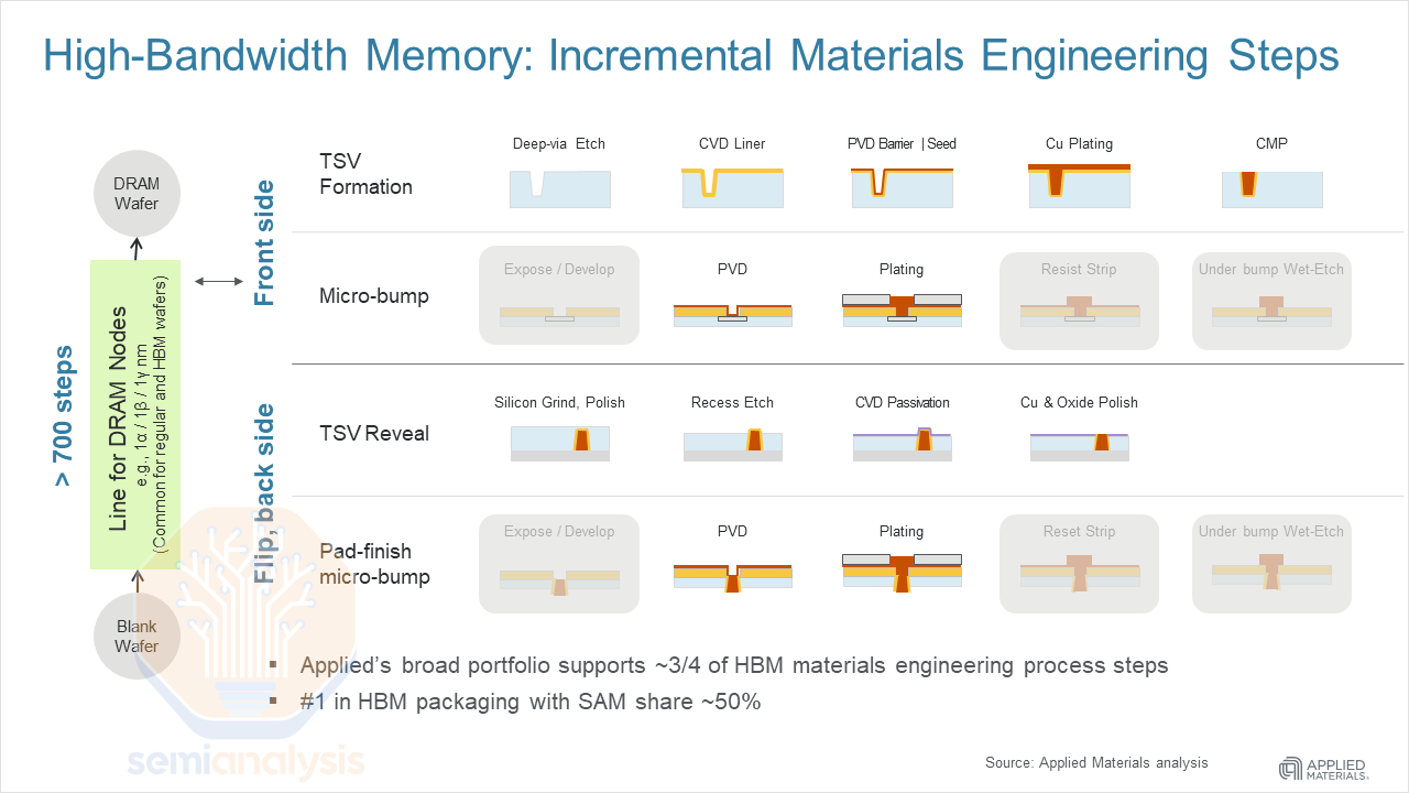
When regular DDR DRAM capacity “converts” to HBM capacity – the main change is the addition of tools for forming the TSVs, and more bumping capacity as HBM wafers are bumped on both sides. Both of these steps are to enable the 3D stack, although they are omitted for wafers used for the top die which only need a single side of bumps and don’t require TSVs.
TSVs require etchers to create the vias, and deposition and plating tools to fill them. To reveal the TSVs, grinders, another etch step, and temporary bonders to attach carrier wafers used in this process are required. This is why HBM capacity is now quoted in terms of TSV capacity, as this is the main incremental set of processes that turn DDR wafers into HBM wafers.
For bumping, this is mainly deposition, plating and stripping. Also, optical inspection tools from Camtek and Onto are available to check that the bumps are not defective and are of the correct profile.
Process Flow: Packaging
The other part of this is back-end packaging which Hynix continues to push forward with MR-MUF which we wrote about extensively here. In short, MR-MUF offers higher productivity and better thermal performance. Hynix’s proprietary (co-developed with NAMICS) molded underfill material offers more thermal dissipation than the Non-Conductive Film that Micron and Samsung use. Hynix has been able to sidestep thermal compression bonding (TCB) because they have found other ways to manage warpage. One of the benefits of TCB is the use of force to stabilize the bonding matter.
The use of force on the other hand increases the risk of causing damages to bumps. With stress applied to bumps, SK can also add more dummy bumps which also helps with thermal dissipation.
The process is also far more productive. A batch mass reflow and single over-mold step are used for joint formation, compared to a complete TCB step for joint formation for each and every layer with TC-NCF.
Process Flow: Yields
HBM is a more technically sophisticated product than other DRAM form factors, especially given the high 3DIC stack. As such, packaging yields are not going to be comparable to what manufacturers are accustomed to compared to their more conventional products. However, yields at the front end are also challenging, and we think yield is more of a problem at the front end. As mentioned above, HBM is not demanding with regards to speed bins, so why is this the case?
The reason goes back to the 3DIC assembly and the TSVs. One of the challenges is the Power Distribution Network (PDN) with the TSVs needing to be able to deliver power up the stack. TSV layout and design is proprietary and one of the main areas of differentiation between the various manufacturers.
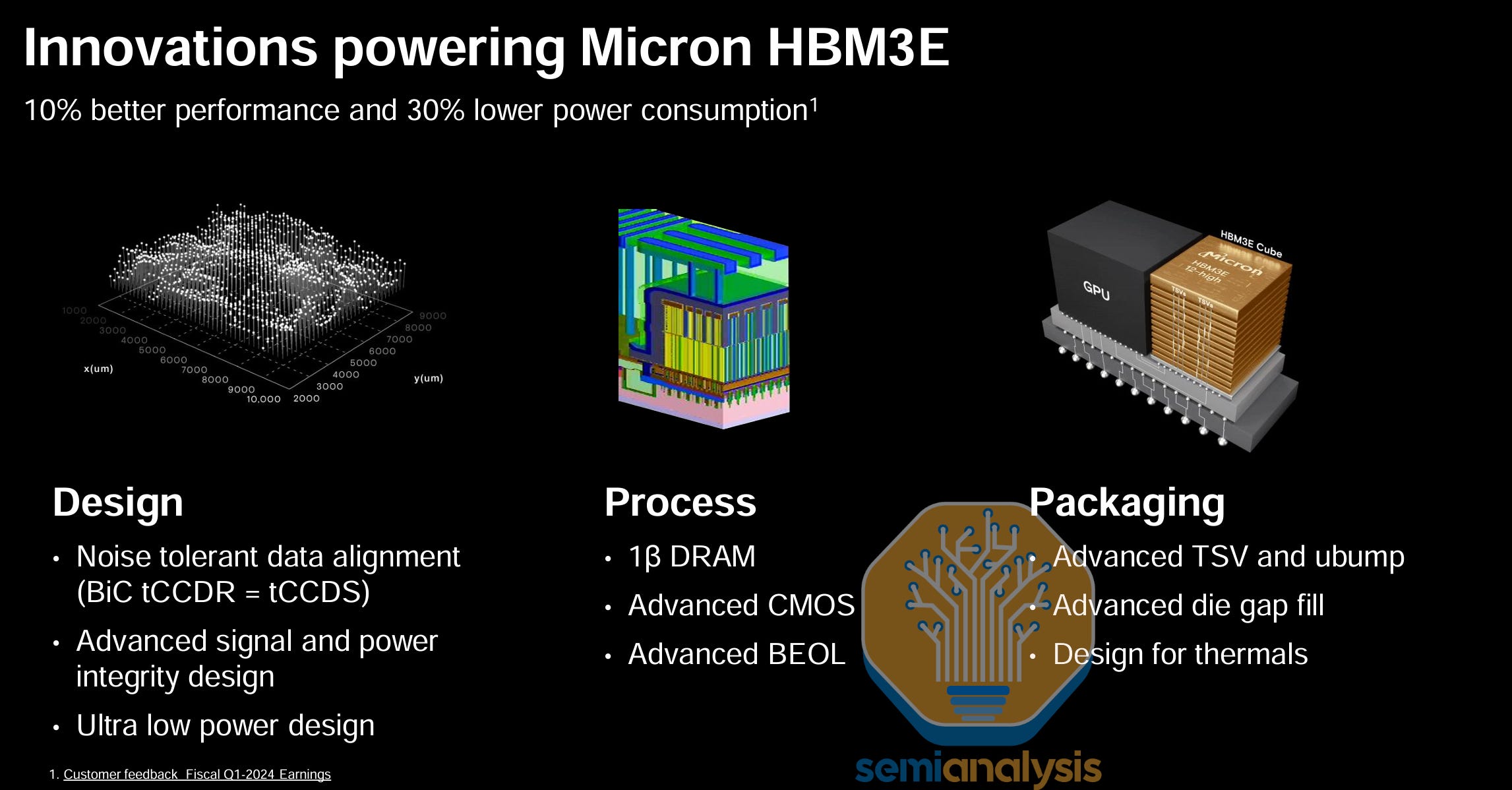
One of HBM's key challenges is delivering power up the stack with power TSVs. Refresh operations especially draw a lot of power, and the design of the power distribution network is important. Hynix’s HBM3E has reduced peripheral area and introduced all-around power TSVs on the die instead of having two banks of power TSVs, thereby increasing the number of TSVs by almost 6x. As a result, SKH has achieved a much lower IR drop, up to 75% lower for VPP.
Similarly, Micron's surprising leapfrog in HBM technology (Micron didn’t even offer standard HBM3) was due to its focus on TSVs and the power delivery network. The TSV network seems likely to be the point of differentiation that allows Micron to claim 30% lower power consumption, though that claim is yet to be verified.
The other thing is delivering the promised speeds within the power and thermal envelope. As with any 3DIC assembly, thermal dissipation is an issue, and DRAM especially doesn’t like heat. As data from hyperscalers have shown, HBM failures are the number one cause of GPU failures, which happen more frequently than other chips in the data center.
All manufacturers have absolute yields well below what they’re accustomed to compared to their conventional memory wafers, so it is a question of relative yields and the end economics. For SK and Micron, yield loss is more than made up for by high pricing, and hence, HBM is margin accretive. For Samsung, yields are even worse. Ironically, their low yields tighten up the total DRAM wafer supply, leading to higher pricing.
This leads us to layer counts. Higher layer counts are harder to achieve. Simplistically if the stack yield of a single layer is x%, each layer’s yield will accumulate to x% to the power of n bond steps (which is just total layers less 1). Take an 8-layer stack with 99% stack yield per layer; total yield will be 92%. For a 12-layer stack, this becomes 87%. Of course, this is overly simplified. Yield degrades at higher layer counts as non-critical stack defects can accumulate. For example, a small but acceptable amount of non-co-planarity at a few layers can result in an unacceptable amount of co-planarity at higher levels.
Process Flow: Bonding Tools, SK Hynix + Hanmi Drama
The bonding or die attach step is a key contributor to yield and thus requires sophisticated tools. With TSV pitches around 40 µm, the bonders must be capable of single-digit or even sub-micron alignment accuracy. Even pressure distribution is also crucial to avoid warpage that will compound over many layers. And throughput of course is important as it drives cost.
Hanmi made an early bet to focus on thermocompression (TC) bonders for HBM, a segment at that time ignored by market leaders Besi and ASMPT. This paid off in a near monopoly in current HBM processes. At SK Hynix their share was 100% until last fall, when Hynix placed a large order with competing tools from Hanwha. Allegedly, they paid Hanwha a higher price for the tools.
This set off a firestorm at Hanmi who, understandably, were upset to see a competitor winning with higher prices despite not being qualified on Hynix’s process for HBM supply to Nvidia, the largest and most important HBM customer.

The dispute reached a fever pitch in early April when Hanmi pulled its field service teams out of SK Hynix fabs. Without service, it would be months if not weeks before Hynix was unable to ship its marquee products. Longer-term it would threaten the entire accelerator supply chain as Micron and Samsung would not quickly be able to fill the capacity void. Hanwha’s tools had not yet been delivered and a batch of ASMPT bonders ordered last fall do not work for Hynix’s HBM3E 12-high. This left the fabs with little choice but to beg forgiveness from Hanmi.
Under enormous pressure, SK Hynix placed a small order with Hanmi in recent weeks. It appears this was more to placate Hanmi than a large volume order, but it was enough to restore field service to the tools. There may not be much more juice for Hanmi to squeeze from their monopoly power, as ASMPT, Besi, and others are rushing to improve their HBM-specific TC bonders.
China: CXMT & Huawei HBM
Export restrictions ban the transfer of all raw HBM stacks into China; however, chips with HBM can still be shipped as long as they don’t exceed the FLOPS regulations. Currently, banned HBM is still being reexported to China through a network involving CoAsia Electronics, Faraday and SPIL which allows end users in China to desolder and reclaim the HBM from GPU packages.
As HBM is one of the key ingredients for accelerators, and with export restrictions threatening to cut off HBM supply, China is naturally pouring resources into domestic development efforts. China has planned 200B USD in subsidies for home-grown semiconductors over the next five years. Expect a material portion will go towards HBM. DRAM national champion CXMT is aggressively expanding HBM capacity, with a large stockpile of tools to insulate from updated export controls (U.S. increased HBM controls in Dec. 2024, Korea more recently). HBM2 8-high will enter mass production in the first half of 2025, with TSV capacity matching Micron’s by the end of the year.
Huawei, which has never seen a high-tech market it doesn’t want to enter, has its own HBM affiliates with XMC (Wuhan Xinxin) producing the HBM wafers and SJSemi (Shenghe Jingwei Semiconductor) packaging them. Current capacity is at R&D scale, not high volume, but is planned to ramp in coming years. Both XMC and SJSemi are entity listed and thus restricted from buying equipment with U.S.-origin content (GlobalFoundries recently got a slap on the wrist despite selling more than $17 million in chips to SJSemi without a license).
HBM Stack Counts – Let’s Get High, to Hybrid Bond or Not?
More layers in the HBM stack means more memory capacity. With each generation, layer counts have gone higher. This stack height has been contained within a 720-micron height cube (the current JEDEC standard) up until now. To fit in more layers, each die (excluding the top die, which needs to be much thicker to withstand handling during subsequent packaging steps) has been made thinner, and the bump gap between the dies has also been made thinner to create more space to fit in more layers. Thinner dies are increasingly difficult to handle and, therefore, more vulnerable to warpage and breakage, which hurts yields.
The main benefit of Hybrid bonding (HB) for HBM is it is bump-less. By eliminating the bump gap this frees up room for more DRAM core layers to fit. This introduces a whole host of new challenges for yield and cost which may not be worth it, especially as HBM doesn’t need the level of interconnect density that hybrid bonding offers. If anything, manufacturers are exploring how much the pad density can be relaxed in hybrid bonding to ease bond accuracy requirements to make the technology more viable for HBM. HB also offers a one off power and heat benefit but the primary benefit is stack height.
HB adoption for HBM has always been a “next generation” technology and the goalposts continue to keep shifting. For D2W hybrid bonding, getting yields to be acceptable is extremely difficult and expensive for a 2 layer. Imagine scaling that problem for 16 layers and higher. The memory players are still very early in their hybrid bonding technology development. In TSMC’s experience, HB adoption has taken a long time to reach volume production and even when the performance benefits are clearer in advanced logic - adoption has taken a long time.
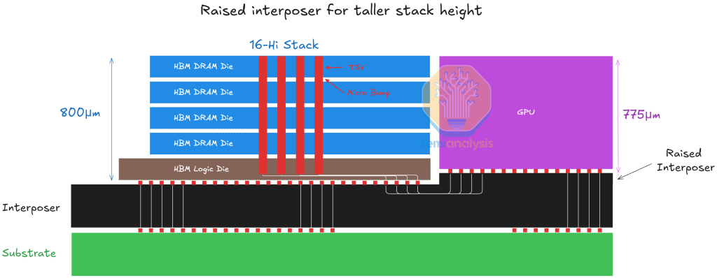
HBM3 and HBM3E are going up to 12-hi stacks and with bump-based interconnect, 12-hi has approached the limit within the current 720um cube thickness. The two solutions to go higher are either bump-less or making the stack taller/thicker. In a blow to hybrid bonding adoption, the latter has been chosen with JEDEC confirming a relaxation to 775 um stack height.
Height relaxation can go even further. 775um is the standard thickness of a silicon wafer. HBM needs to be the same height as the logic die it is co-packaged with. To have something higher than a 775 um stack, the logic wafer would also need to be thicker and the current equipment is not designed to accept thicker wafers. One potential solution could be to raise the molding of the interposer underneath the logic to raise it and ensure coplanarity with the neighboring HBM, though this lengthens the traces and implementing silicon bridges for interconnect will not be straightforward.
While initially there was more talk about HB implementation for HBM4, this has been shifted back to 4E. Recently, both Hynix and Micron have been far quieter on HB adoption, while Samsung is the loudest. This is typical for Samsung which often promotes the most aggressive technology implementations in attempts to catch up, only to expectedly fail on execution. This leads to them falling even further behind.
While 16 layer is solved by the higher stack height, to get to 20 layer and beyond, there is likely a further reduction of the bump gap and more wafer thinning, or we simply cap out at 16 layers. With higher stacks you can get more density but more stacks offer bandwidth and density.
Throughput Optimized: I/O is the Lifeblood of the AI Accelerator
The key defining feature of an AI accelerator is they are highly parallelized and optimized for throughput. Accelerators are designed to maximize the total number of operations an accelerator can perform per second by sacrificing the complexity of these operations. Most accelerators focus on multiplication and addition operations for General Matrix Multiplication (GEMMs), which dominate AI training and inference workloads. This compares to CPUs, which are also focused on how many instructions per second they can execute, but CPU cores are much “smarter,” which requires far more circuitry and area. Therefore they are designed to execute a broad range of more complicated tasks but at much lower throughput.
The implication is that AI accelerators need a lot of off-chip bandwidth for memory and the scale up and scale out fabrics. Bandwidth is needed to move the processed data off-chip whilst also feeding the accelerator unit with more data to process. Without sufficient bandwidth, the XPU’s compute elements will be left unutilized, defeating the purpose of having all this parallel computing power available. Let's start with memory needs
Memory content increases
To deliver more performance - increasing memory capacity and bandwidth along with FLOPs has been paramount and easily observed in accelerator roadmaps. There are 3 dimensions where capacity and bandwidth are scaling:
Newer generations of HBM deliver higher bandwidth through faster signalling speeds, and denser core die
Adding the number of layers per stack increases capacity. We are on the cusp of 12-high HBM becoming the mainstream configuration
Adding more HBM stacks per package adds more bandwidth and capacity
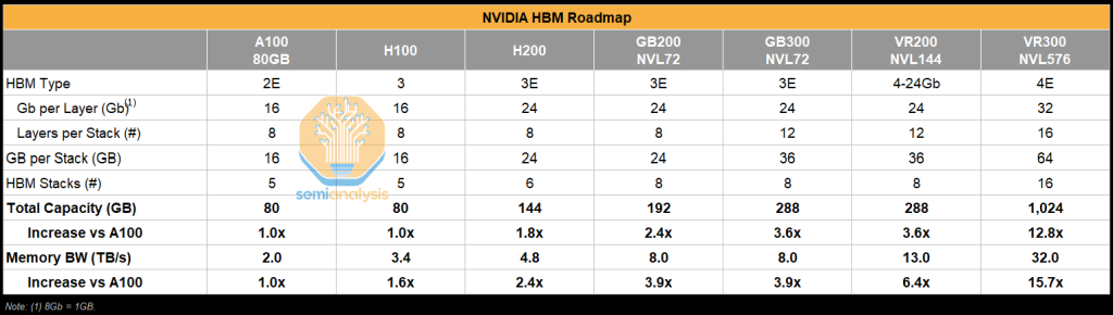
Here we can see this in Nvidia’s roadmap. HBM capacity explodes from the A100’s 80 GB of HBM2E to a 1024 GB of HBM4E for Rubin Ultra. Memory bandwidth per chip also increases dramatically. From Ampere to Blackwell Ultra, the biggest absolute and relative increase in the bill of materials comes from the additional HBM content- benefitting the memory vendors (primarily SK Hynix).
This is related to the need for non-memory I/O as well. Scaling up more GPUs in a single memory-coherent domain delivers more aggregate memory capacity and bandwidth. This allows scaling inference of larger parameter models and support for much longer context lengths that are becoming prevalent in reasoning models and complex workloads.
Just as Parkinson’s Law observes that work expands to fill the time allotted, modern AI follows a “memory‑Parkinson” dynamic in which neural‑network architectures relentlessly grow to occupy whatever HBM becomes available. Each generational bump in HBM capacity and throughput, whether 80 GB at 3 TB/s on H100 or 192 GB at 8 TB/s on GB200, quickly encourages designers to increase parameter counts, context lengths, and KVCache footprints, nullifying the headroom that seemed ample only months earlier. Techniques once deployed to squeeze models into tight budgets (activation checkpointing, optimizer off‑loading, weight quantization) are relaxed as soon as new HBM space appears, until the memory wall is hit again and efficiency tricks must be rediscovered. In effect, the mere presence of larger, faster HBM does not yield sustained slack; instead it resets the baseline for “reasonable” model size, ensuring that capacity and bandwidth remain limiting factors despite silicon advances. Essentially, as AI chips get more HBM, developers immediately build larger models to fill it, so memory is always the next bottleneck. Let's go through how HBM is used, and where the pressures are.
HBM Usage in Inference
In LLM inference, all the model weights reside permanently in the on-package HBM memory so the GPU can fetch them without delay. Alongside the weights, HBM also holds the KVcache. Each time the model is asked to produce the next token, the GPU first reads the weights from HBM and simultaneously retrieves the entire KV cache so it can compare the new token against the conversation history during the self‑attention phase. After computing, the GPU appends a fresh key and value for the newly generated token back into HBM, enlarging the cache. This is very demanding on bandwidth as every token decode step repeatedly reads both the static weights and the ever‑growing KV cache. If memory bandwidth is not able to move this data at terabytes per second the GPU spends more time waiting for memory than performing computation. This is what happens in reality, as bandwidth significantly overwhelms the compute intensity of token decode, making most LLM inference workloads memory bandwidth-bound rather than compute bound.
As models improve, they have increased in horizon lengths. What this means is that models are able to think, plan, and act for longer periods of time. This rate of increase has been exponential and has already manifested itself in superior products. Deep Research from OpenAI, for example, can think for tens of minutes at a time, while GPT-4 mustered mere tens of seconds.
As models can now think and reason over a long period of time, the pressure on memory capacity explodes as context lengths regularly exceed hundreds of thousands of tokens. Despite recent advances that have reduced the amount of KVCache generated per token, memory constraints still grow quickly. One way to deal with this has been to serve reasoning models at lower batch sizes which is harmful to economics.
The main driver of AI progress is Reinforcement Learning (RL) and a huge part of the RL paradigm is inference. As an example, often what is needed for RL is synthetic data satisfying strict requirements, which means conducting many GPU-hours worth of inference to generate data that is later filtered by another model. Another example of heavy inference loads is RL for hard-to-verify tasks like creative writing. Unlike code, which can be checked and verified easily, things like creative writing, legal work, and teaching cannot be verified trivially. The way to get around this, and thus to get a signal to reinforce and improve the model, is to have another model judging the answers. This LLM-as-a-judge is then given a rubric, currently hand written but soon to be automated by LLMs, which it uses to grade the answer.
KVCache offload
There are various algorithmic or setup improvements that are designed to reduce pressure on scarce HBM. One technique is offloading the KVCache to a cheaper and more available tier of memory such as conventional DDR or even storage.
Today, KVCache offloading is already commonly used . Nvidia has a framework for this called Dynamo Distributed KVCache Manager. Conceptually this is not so different from the multiple tiers of memory available in general purpose CPUs: extremely fast but low density L1/2/3 Cache and slower but high density DRAM. In an AI system, where the where the KVs are stored based are managed based on frequency of usage. A well-optimized system keeps all currently used KVs in HBM, infrequently used KV in DDR, and very rarely used KV in NVMe.
Just like how DRAM is not cannibalistic to L1/L2/L3 cache demand for CPU, HBM and DDR/SSD offload do not compete with each other directly. In fact, for most modern LLM workloads, the prefill speed (aka the rate at which KVCache is produced) is typically slower than the transfer rate to DDR or NVMe SSD, meaning KV rarely ‘lives in HBM’ in their entirety. They get produced and evicted or sent to the decode node to be used to produce the next token. Mostly it’s the system prompt that is used for every user that is kept in HBM as well as other hot KVs such as the active sequence window and some prefetch buffers.
As for whether DDR or NVMe is used, it depends on workload needs and size of workload. It also depends on how often the workload is cycled as frequently cycled KVs are not a good fit for the limited write/rewrite tolerance of NAND. Agentic use cases that use tool calling to pull in documents and data at very low latency and high cycle rates today further push caching from NVMe to DDR. These are architectural and user experience tradeoffs to consider, rather than direct substitutes to each other.
As use cases evolve, there may be different hardware setups used for different inference needs. For example, querying a fixed code base or document would benefit from accessing larger amounts of KVCache per user per GPU as the memory demands of those user behaviors is extremely high compared to normal chat.
HBM for Pre-Training
For traditional pre-training, everything the GPU needs for a forward‑and‑backward step passes across HBM. First, the model’s weights are stored in HBM so each layer can read them quickly while computing the forward pass on a batch of data. As every layer processes the batch, it writes intermediate activations into HBM so they are available later. Once the forward pass finishes and the loss is calculated, the backward pass begins: the GPU revisits those stored activations and weights, reading them from HBM to compute gradients. The resulting weight gradients, plus any auxiliary optimizer statistics (for example, momentum or variance terms in Adam), are also written to HBM. Finally, the optimizer reads those gradients and statistics from HBM to update the weights in place, ready for the next iteration. However, training operations require more compute relative to data transfer, meaning training is more often compute bound. But as mentioned above, RL is now key to improving model capability - so what was traditionally achieved with pre-training is becoming more like inference in the form of reinforcement learning.
The rest of this piece will discuss OpenAI's ASIC project, shoreline area challenges, the revolutionary change coming to HBM4 with custom base dies for HBM, the advantages on PHYs, memory controller offload, repeater PHYs, LPDDR + HBM combos, and various beachfront expansion techniques. It will also discuss SRAM, compute under memory, supply chain implications, and Samsung's struggles.
 |
|