

High-NA is Here (for R&D), EUV Cost, Pattern Shaping Gaining Share, 6x12" Mask, Metal Oxide & Dry Resist, Hyper-NA
SPIE Advanced Litho & Patterning 2025 Round-Up
“Lithos Graphein” is back as a guest contributor to this report. Follow him on twitter @lithos_graphein
If TSMC is “the most important company in the world,” according to President Trump, then EUV lithography tools are surely “the most important machines in the world.” Does that make SPIE Advanced Lithography & Patterning the most important conference in the world? Not exactly, but it’s at least a good opportunity to see the latest progress in EUV and advanced logic.
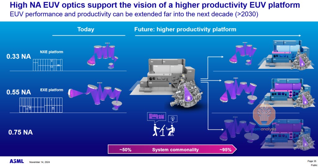
In this report we’ll cover the technology highlights and market implications from this year’s conference. High-NA was a main topic as real wafer volumes are being run on customer (Intel) tools. Complementary patterning techniques such as pattern shaping (AMAT Sculpta and TEL Acrevia) and directed self-assembly are picking up steam. And ASML itself is already on to the next topic: hyper-NA for the CFET era.
Manufacturing Readiness of High-NA EUV
The highlight keynote was delivered by Steve Carson of Intel on the manufacturing readiness for their two fully installed high-NA EUV tools. As a recap, Intel has gone all in on high-NA EUV, installing the first shipped tool, the EXE:5000, over a year ago and accepting a second shipment shortly after to get early learnings ahead of the competition.
Intel clearly views high-NA EUV as being a critical part of their product strategy for launching their 14A node, although they have said 14A is possible with only low-NA. With a total of 30,000 wafers now exposed across two fully installed tools, they are in the best position to assess the viability of the new scanner in a manufacturing environment. The stated goal was to bring up a development pilot line with the new high-NA EUV system in record time, avoiding the slow ramp that plagued low-NA EUV.
Several first-of-a-kinds for a new scanner technology were undertaken by Intel and ASML. The normal scanner build process is to assemble it at the ASML Veldhoven factory, where the fully assembled tool is tested to customer’s and ASML’s agreed specifications. The machine is then disassembled and shipped to the customer’s fab for install and reassembly. For the first high-NA tool, the factory integration and test were skipped. Instead, the first fully built tool testing was done directly at Intel.
This has not been done before and is unheard of for the first unit of a new scanner technology – the high-NA scanner is substantially different than low-NA. ASML and Intel collaborated on this process closely as much of procedures and methods for bringing up a tool and making it reliable were being learned for the first time.
However, a functional scanner alone is only a piece of the high-NA puzzle. The pilot line also required process, reticles (masks), and Optical Proximity Correction (OPC) to be ready on the aggressive 14A timeline. This is especially difficult as all 4 elements are interdependent, which means development must be done serially. This is where Intel was forced to innovate and parallelize as much as possible.
The process portion includes photoresist, where Intel used both low-NA NXE systems and Berkeley’s Microfield Exposure Tool to characterize and down-select the photoresist to be used with high-NA. The etch process for transferring the pattern from the resist down into the underlying materials stack is also normally decided at this point.
OPC is a complex software suite that is used to convert a chip design into complex shapes on a lithography mask. Typically, an OPC model would be calibrated using the actual scanner and POR (process of record) resist and etch to print real wafers. OPC models for device masks, often referred to as a “keyword”, require many of the process details to be known. They contain an etch bias table, thus, the etch process must have first been developed and characterized. The thru-pitch bias for a given illumination pupil, unique to the new scanner is also characterized for the new resist.
But at this point the high-NA scanner was not available. So Intel developed a novel method of calibrating OPC models without true wafer data. Instead, they used a combination of simulation and low-NA exposures that was extrapolated and used to tune a high-NA OPC model. This isn’t normally done as OPC models will have poor accuracy without calibration on wafer data, but Intel proved that it is possible.
The OPC model was necessary to make high-NA reticles, which have smaller features and the new anamorphic setup versus low-NA. With OPC taken off the critical path, the reticles could be produced in time to meet scanner qualification and run the pilot line almost immediately. Traditionally this process takes many months after scanner acceptance – here Intel and ASML reduced it to nearly zero. A bring-up time this short on a brand new scanner technology is unprecedented.
High-NA Imaging Results
With the scanner installed and masks in hand, Intel could characterize the tool. The basic metrics of source power and reliability were vastly exceeding targets for a new scanner system. Source power was 110% of the target, the first time a new EUV system has exceeded the initial target. For comparison the NXE:3300 development tool was just 15% and the NXE:3400B production system 50% of their target source powers at first shipment. ASML has actually gotten ahead of their source roadmap. Reliability was at 85%, which was also significantly better than any prior systems at this point in development.
Overlay performance was impressive – 0.6nm aligned to a low-NA tool. This exceptional performance across multiple tools is often taken for granted but is part of what makes ASML singular. It gives chipmakers flexibility to mix and match toolsets with good results, rather than limiting critical layers to the same tool or even same wafer chuck. Competitors are miles (nanometers) behind on this.
This overlay result was sufficient for Intel and ASML to declare that high-NA has no penalty for stitched fields. This has been a big concern as the high-NA optics limit field size, so stitching is required for large dies such as a GPU. Despite their declaration, it’s still an open question if fabless customers will accept a stitched die. Likely there will be design rule limitations in the stitching areas at the very least.
The consensus on photoresist thickness is that high-NA lithography will require significantly thinner film coatings which impacts the required optical depth-of-focus. Intel was able to make an assessment on this crucial process parameter that impacts manufacturability. Focus control for the new high-NA tools outperformed the low-NA NXE system which meets the target specifications.
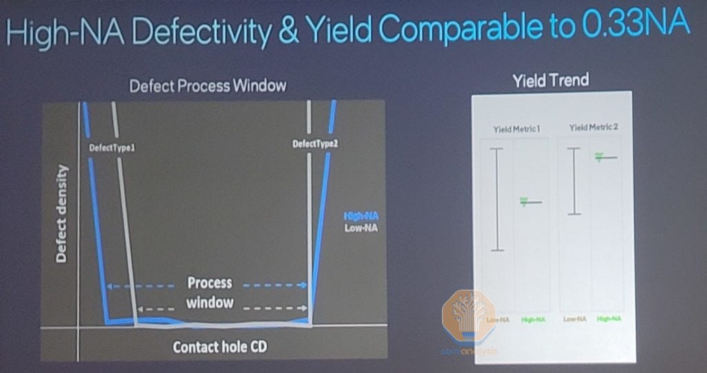
Along with the core lithography performance, Intel shared early device data for metal and contact hole layers. Both are critical layers at 14A where high-NA EUV could tip the yield scales. For metal, the comparison used a single high-NA exposure to replace an existing metallization scheme comprising three low-NA exposures and more than 40 process steps in total.
It should be noted that the low-NA process uses pitch splitting with self-aligned double patterning (SADP) to shrink beyond low-NA EUV single-exposure limits. Intel refers to this as self-aligned litho-etch litho-etch (SALELE). SADP requires many process steps as it relies on ALD and a series of etches to split the metal pitch down to the desired geometry. The other two EUV exposures are used for cut masks that trim the lines from pitch splitting and also pattern the larger pitch metal features. High-NA replaces all this with a single exposure and many fewer process steps.
For the contact-hole (CH) layer, Intel shared yield data showing similar yield with high-NA to an existing low-NA multi-patterning (LELE) process. For context, the early masks used to measure the health of a layer are notoriously bad at delivering promising results. Typically, a number of iterations of OPC and mask spins are required to get a live yield signal. So comparable yield between high-NA and the mature process is impressive at this stage.
They did not share the number of low-NA mask steps, nor the total number of process steps (more on this later). Our assumption is that this would be two passes of low-NA memorized into a hard mask prior to final etch transfer and metallization.
Last, Intel finished with a call to action on new mask infrastructure (more on this in the cost analysis section below) and a bold declaration that both of their high-NA EUV systems were now “in production.” This term means running test wafers on a proven process, not that high-NA scanners are running commercial products.
Likely the proven process used here is 18A, as it will be in the final stages of development and taping out mask sets with prospective customers, with the process steps mostly frozen. This serves as a convenient baseline for experimentation by swapping in high-NA for one or more critical layers. Comparison with the low-NA POR for 18A, well characterized at this point, gives valuable feedback towards 14A development.
This same concept is used to test many new technologies to vet them prior to production. In the case of low-NA EUV at 7nm, it was used to generate yield learnings before the cost made sense. The initial source power at that time was too low to make EUV competitive with DUV quadruple patterning.
High-NA Cost
ASML’s latest high-NA system, the EXE:5000, weighs an astounding 150 metric tons and has a comparable price tag of nearly $400 million. It’s close to twice the price of a low-NA system, which directly translates to a higher cost of operation and ultimately wafer cost.
As we’ve discussed in our report on high-NA vs. low-NA multipatterning, equipment decisions are based on cost. While reducing complexity is good, it is not cheaper in every case. This is what was missing from Intel’s talk. Is it cheaper than low-NA LELE or SALELE?
Given they are “in production” with branch high-NA run paths comparing directly to these alternatives, they must know the answer. Intel along with imec and IBM are all pushing for high-NA to be adopted at the 14A node; however, being too early with a fleet of scanners to run your production line—at a price tag in the billions—could be just as detrimental as being too late with a new enabling technology.
SPIE organizers have a habit of placing the most important talks on Thursday afternoon, and one of them was by Luciana Meli from IBM, who presented the only talk addressing the 150-ton elephant in the room—is high-NA cost-effective?
IBM presented several key findings based on simulation and their work at the Veldhoven high-NA EUV lab. First, they determined the 14A layers with largest potential benefit from replacing multiple low-NA exposures with a single high-NA pass:
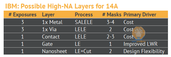
Their cost analysis focused on SALELE as it offers the highest cost savings potential, replacing three or four low-NA exposures with one high-NA. Details here filled in a few key items left out of Intel’s talks. First, the number of process steps in SALELE is roughly twice those needed for a high-NA single exposure. Recall that Intel indicated SALELE was approximately 40 process steps for their three mask process; thus, the number of steps in a high-NA module is still significant. For cost, IBM claims a four mask SALELE process is 1.7-2.1x more than a single high-NA pass. Not a surprising result but a good data point on cost – it was expected that high-NA single exposure would be cheaper than triple or quadruple low-NA exposures.
However, IBM also helped confirm our modeling on high-NA versus low-NA double patterning, suggesting that the low-NA option is cheaper. Their data shows a single high-NA exposure costs roughly 2.5x a single low-NA exposure. This strongly suggests that any cost-per-pass benefits for high-NA wouldn’t kick in unless three low-NA masks are reduced to a single high-NA.
Another interesting finding from IBM’s presentation was that a high-NA single exposure for a metal process might have trouble meeting the metal tip-to-tip design targets. Note that a low-NA SALELE process excels here with a dedicated cut mask defining the tip-to-tip features. IBM suggests that directional etch process technology, such as Applied Materials Sculpta tool, would be needed to augment this shortcoming – more on pattern shaping in a few sections.
High-NA 6 x 12” Mask
The last slide of Intel’s plenary talk included a call to action for large high-NA masks. They’ve been beating this drum for a while but for good reason: a 6 x 12” mask, twice the 6 x 6” that has long been industry standard, would improve the scanner productivity by 23-50%.
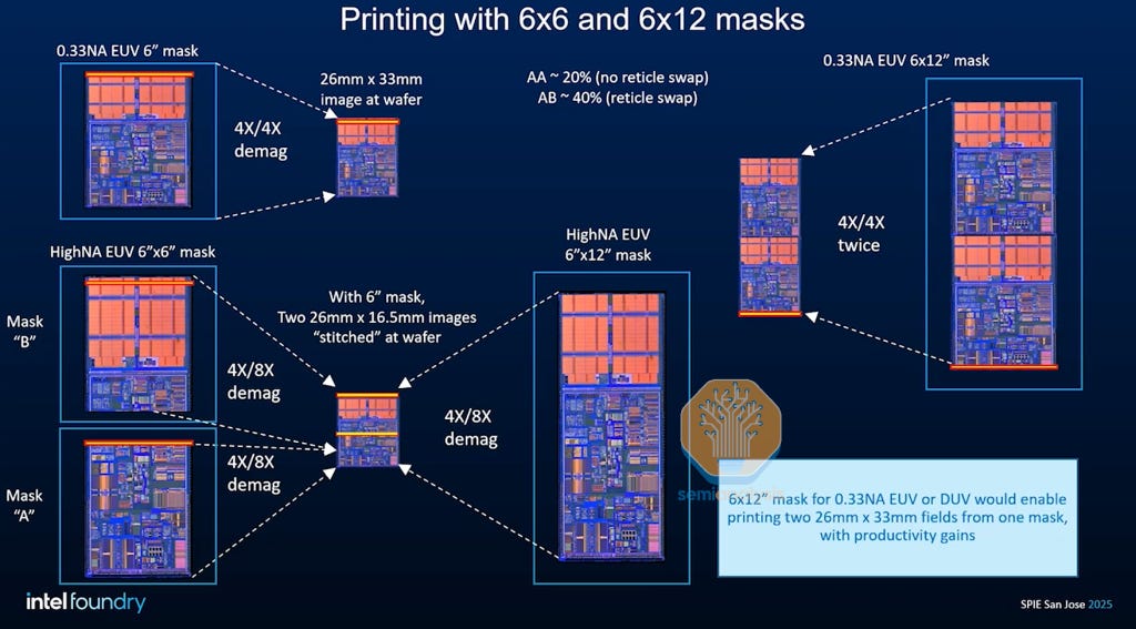
It enables full-field exposures, eliminating the stitching issue along with the throughput gains. Assuming a reasonable increase in scanner cost, this would swing the economics of critical layers to clearly favor high-NA.
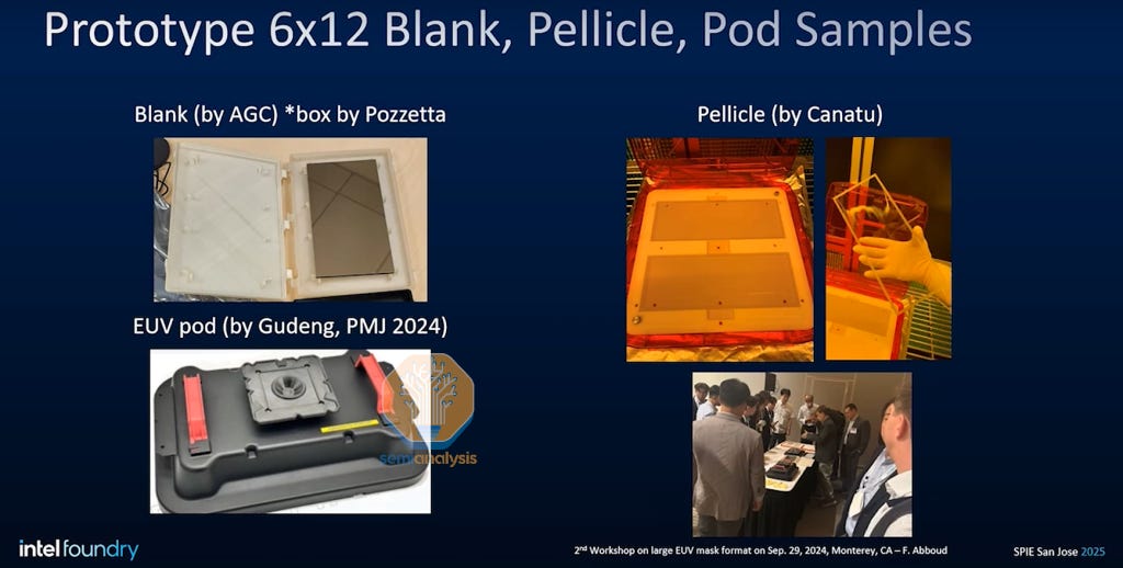
While Intel and others say the mask ecosystem sees no major showstoppers for large mask, the tipping point really depends on ASML. While the CEO Christophe Fouquet’s plenary at SPIE EUV last year was positive towards large masks, it wasn’t on the roadmap and the company didn’t formally state they can or will develop the capability. This year, ASML’s plenary talk went further, stating that the larger “ecosystem is progressing,” “impact studies were ongoing” and that it may be introduced sometime “early in the next decade.”
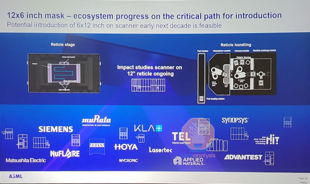
This is not a minor change. The 6 x 6” mask size has been standard since the start of projection lithography in the 1980s. All the tooling: blank manufacturing, resist coating, e-beam writing, mask cleaning, fab handling, etc. must be rebuilt for the new mask size. It’s the equivalent of moving from 200mm to 300mm wafers (recall that an attempted move to 450mm failed a decade ago). The timeline is surely beyond the ramp for the 14A node.
For ASML, the 6x12” mask is at odds with their core EUV systems strategy where they desire to make the NXE, EXE, and future hyper-NA systems on a common platform to streamline their production, one of which is the reticle stage and handling system. A large mask would require significant changes to these modules and probably disrupt the commonality.
A large mask is also not directly in ASML’s economic interests. If the choice is between two regular mask high-NA scanners or a single large mask tool, selling two complete scanners is probably 200-300M more revenue for ASML. Developing a large mask tool would be extremely customer-friendly.
High-NA EUV: Insertion at 14A or 10A?
At 14A, high-NA only offers a cost advantage in a few metal layers where it would replace three masks in Intel’s process. Note that TSMC is not necessarily using triple EUV exposures in its A14 process, this is specific to Intel. In other layers, Intel notes, it offers design flexibility and process simplification – advantages that are tangential to cost.
Is cost reduction on just three layers worth the risk of early insertion for a new technology? The reduction is real but small as a percentage of the overall chip process that is on the order of 100 layers. Intel itself has even said publicly that 14A is feasible without high-NA, especially if customers were to demand it. But most signs so far point towards Intel adopting high-NA in critical layers at 14A. The inertia in the organization is probably too strong to change course now. And should the 6 x 12” mask be ready for a potential 10A process, making the economics very favorable, Intel would potentially benefit from early adoption. Its learnings and expertise on high-NA at this point are far ahead of competitors.
Metal Oxide Resist
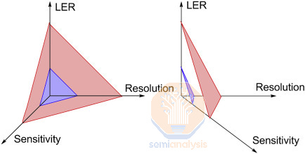
Metal-oxide resist (MOR) has been the “next up” EUV photoresist platform for a few years now. MOR resists offer much better Resolution-LER-Sensitivity (RLS) performance versus the mature organic chemically amplified resists (CAR). Sensitivity and line width roughness, or CD variance, are especially important for EUV because it’s photon limited. At the 13.5nm wavelength, relatively few photons are emitted by the source, but they are much higher power relative to DUV wavelengths. Small improvements in dose sensitivity can have a big impact on throughput and therefore operational costs.
However, as with any new technology, a photoresist platform change requires a lot of momentum to trigger industry-wide adoption. For existing nodes, the benefit was not large enough to induce a change.
It looks like MOR’s time has finally come with the introduction of high-NA. Depth of focus is also one of the key drivers as it decreases with the square of numerical aperture (NA); meaning the high-NA scanner has a very small depth of focus. DoF is also affected by the illumination pupil, which must be optimized for a certain pattern to produce the best image. Unfortunately, the best pupil for smaller and smaller patterns often reduces DoF. The combination of lens NA and illumination pupil both reducing depth of focus produce a tipping point where very thin photoresist films are unavoidable.
The resist thickness must be smaller than the depth of focus so that the image is in focus through the entire height of the resist, or else the resulting pattern in the resist will be poor quality. Here is where a thin MOR resist will excel over thin CAR resist. The conventional CAR resist platform utilizes an organic acrylic polymer backbone (Carbon-Carbon chain) as the basis to block the etch for pattern transfer into a hard mask, such as Silicon Nitride (SiN). A thin organic polymer film doesn't have sufficient etch resistance to survive pattern transfer; however, a metal oxide resist provides much better etch selectivity to pattern transfer into most hard mask films. Therefore, MOR resists provide both better optical and etch performance over CAR.
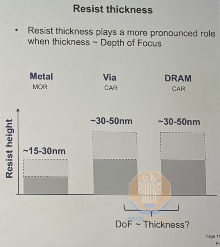
Taking the example of vias, tightly patterned holes that will be filled with metal to form interconnects between metal layers, the crossover point looks to be somewhere in the range of 30nm pitch. Vias will probably scale to this pitch ~2 nodes from now, at the A10 process. This matches with our expectation for when it is economical to introduce high-NA. In other words, it will probably make sense to adopt MOR at the same time as high-NA for a small number of critical layers like metals and vias. Most SPIE papers this year with high-NA exposure data used MOR rather than CAR.
Wet vs. Dry: Resist Coating
Additional research is ongoing that will decide the war for the future of photoresist. To be decided is whether wet or dry application and develop will be used for MOR. TEL is the incumbent here with wet spin-coat application and wet develop both the current standard, with the processing done in their track tools. Lam is attempting to take market share at critical layers with dry resist deposition and etch to develop, both done in Lam’s tools separate from the traditional litho cell.
Winners are starting to emerge in research results. Below, we’ll discuss which of Lam or TEL is likely to win market share. We’ll also cover the next generation of pellicle technology, critical for reducing low-NA EUV costs, complementary patterning techniques like pattern shaping and DSA, along with the potential successor to high-NA: hyper-NA.