

The EDA Primer: From RTL to Silicon
Laying the Groundwork of the Current Chip Design Paradigm
AI demand has been driving the explosion in compute over the past few years, resulting in chip designs getting ever more complex, with silicon area and power per package seeing continued growth as designs push for even greater performance. With each successive generation, new process nodes with more design rules and restrictions further increase chip design costs.
At the same time, the rush to bring compute into the market as quickly as possible has put design teams under immense pressure to compress timelines and speed up validation cycles from years to months. If you’re not fast, you will get lapped up and beaten by your competitors. Even a 3 month delay means billions of dollars.
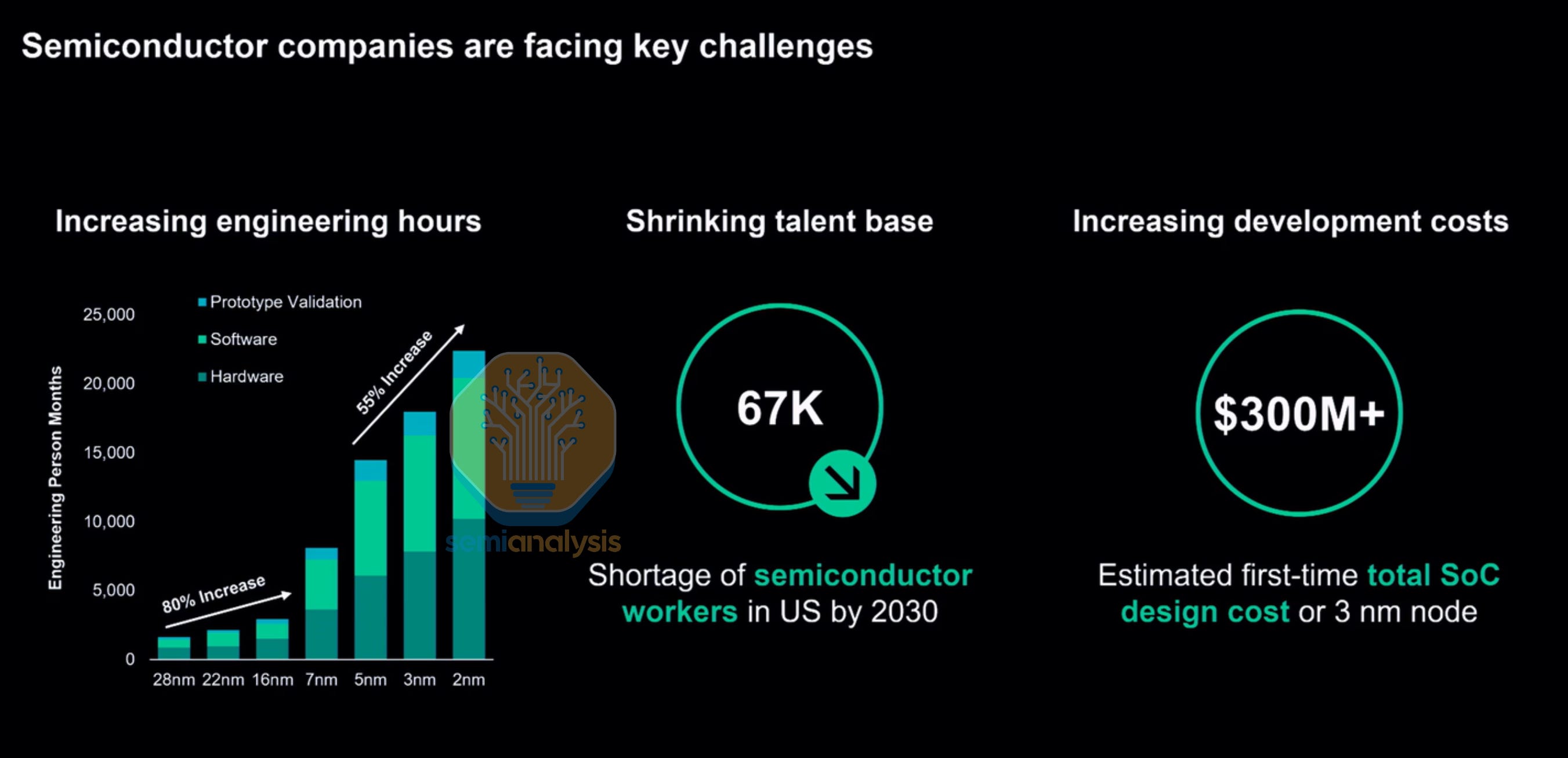
All this is happening while the engineering talent base is shrinking. Lucrative salaries and flexible working arrangements have enticed most students into the Software and Information Systems tracks, resulting in a dwindling number of Electrical Engineer graduates that could enter the chip design workforce. Siemens presented the engineer-hours demanded of these numerous complex AI accelerator designs that far outstrip the engineering talent coming into the workforce.
One-third of the current U.S. semiconductor workforce is over 55. The pipeline of new graduates is nowhere close to filling that gap. Even Apple is actively funding education programs to encourage uptake in engineering. While their New Silicon Initiative has contributed to increasing interest and number of EE graduates, it barely moves the needle compared to the explosion in manpower requirements as transistor count grows at a Moore’s Law pace.
With this trifecta of increasing chip complexity, compressed design timelines and a shortage of engineers, a massive bottleneck has formed at the design stage. The latest AMD MI455X packs 320 billion transistors across 12 logic dies on 2nm and 3nm processes with advanced Hybrid Bonding 3D die stacking, HBM4 memory integration and high speed 224G SerDes. Designing something at this scale is not a matter of hiring more engineers or buying more verification servers. It tests a company’s tooling, methodology, and human capital organization as to whether the design succeeds or fails.
After spending hundreds of millions of dollars on a new SoC design, there is no guarantee the chip will work. Multiple steppings are usually required that need new mask sets, with A0 rarely going into production. When a single advanced mask set costs tens of millions of dollars, every respin is a gut punch to the balance sheet. Furthermore, it adds months to the schedule for high volume production start.
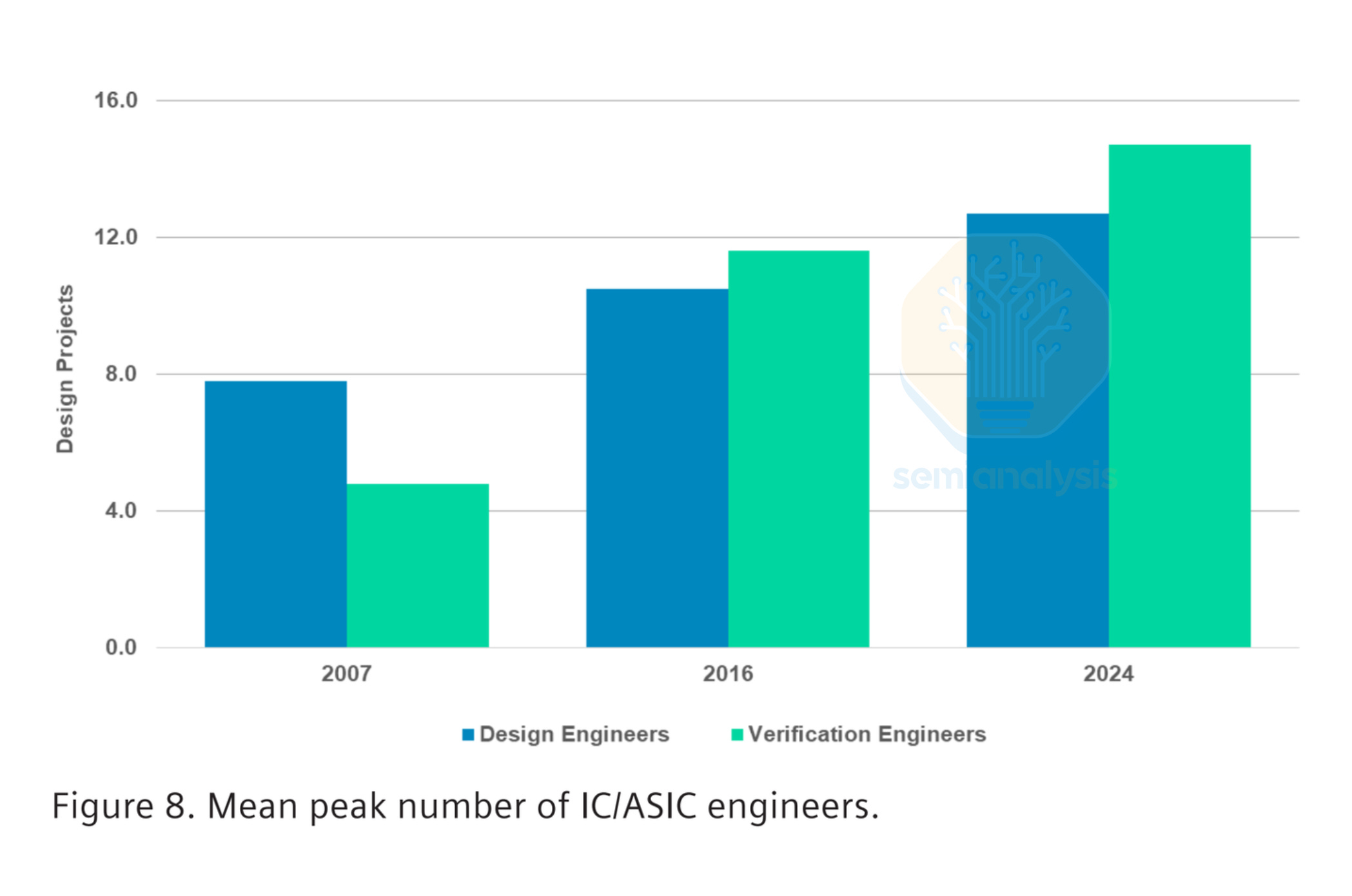
As designs get more complex, testing is becoming more important to ensure all modules within a chip are interoperable and locally sound. Verification, the process of proving a design does exactly what it should before committing it to silicon, now consumes up to 70% of total project effort, depending on the design. Verification engineers are the fastest-growing job category in chip development, and the industry still cannot hire them fast enough.
While chip complexity grows at roughly 50% per year, driven by new nodes and larger SoCs, design productivity improves only about 20% each year. This design productivity gap means every new generation of silicon demands exponentially more engineering effort, more compute, and more sophisticated automation.
The semiconductor industry’s ability to keep building more powerful chips depends not on physics or lithography alone, but on EDA (Electronic Design Automation) software. These tools effectively translate human intent into manufacturable silicon. Without EDA, no chip designed after the mid-1980s would exist.
This primer is your guide to EDA in the semiconductor industry. In this first part, we will walk the entire journey from RTL (Register Transfer Level) code, the high-level hardware description language that engineers actually write, all the way to manufactured, packaged silicon. We will name the tools, explain the tradeoffs, and show why EDA is one of the most consequential and underappreciated sectors in technology.
In part 2, our EDA Market Primer dives deep into the business of EDA, profiling the major companies (Synopsys, Cadence, Siemens) and their revenue and business models. We provide comprehensive market analysis and monitoring the Chinese EDA effort, as well as IP licensing and outsourcing to design partners and the transition to Customer Owned Tooling (COT) with hyperscaler ASIC designs.
EDA Market Primer - Market Dynamics, Cadence, Synopsys, Siemens, China EDA Rise

Every advanced chip on earth is designed using Electronic Design Automation (EDA) software from three companies. Synopsys, Cadence, and Siemens EDA bridge the gap between what a chip needs to do and what a foundry can manufacture, translating billions of transistors into manufacturable silicon.
Part 3 then assesses how AI is disrupting the EDA industry, covering the full gamut from startups and engineer dashboards to agentic chip design flows from NVIDIA and the big three. The concept of using AI accelerators to create superhuman designs that go into future AI accelerators is the most exciting development that our industry has seen in decades. Stay tuned as we cover the incoming revolution in chip design.
A Brief History: From X-Acto Knives to the Big Three
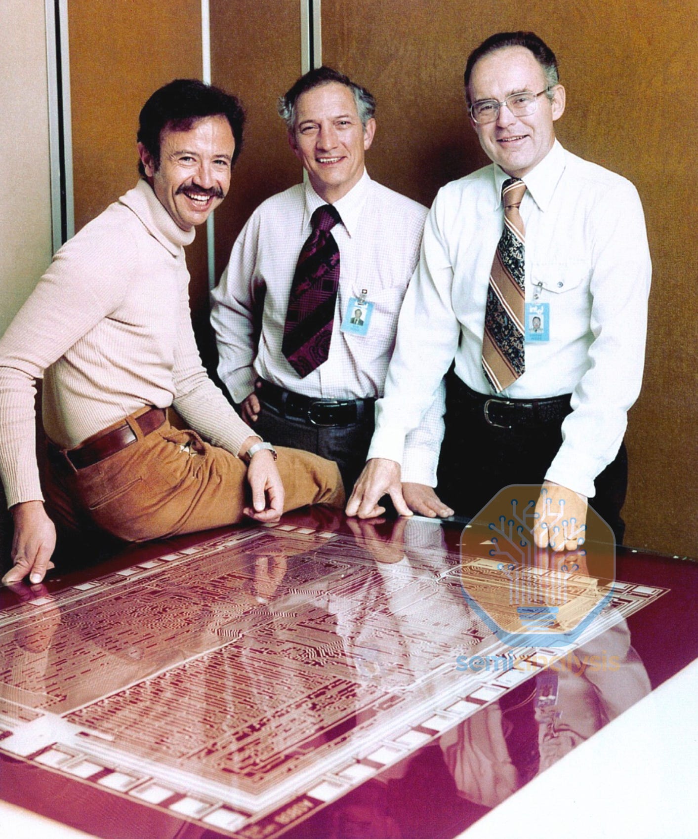
In the 1960s and 1970s, designing an integrated circuit meant drawing it by hand. Engineers sketched layouts on graph paper, and technicians transferred those sketches onto sheets of Rubylith, a red cellophane film laminated onto clear Mylar. Using X-Acto knives and light tables, they cut away sections of the film to define each layer of the chip. The finished masters were then photo-reduced up to 100 times to create production photomasks. A single slip of the blade could ruin weeks of work. This was the standard design process up to and including the Intel 8080 with its Rubylith pictured above.
The first step toward automation came in 1971, when Calma shipped its Graphic Design System (GDS) to Intel, allowing engineers to digitize and edit layouts on minicomputers. In 1978, Calma released GDS II, whose stream file format became the de facto standard for exchanging mask data. Remarkably, GDS II remains the dominant interchange format today, nearly five decades later, alongside its modern successor OASIS.
The EDA industry as we know it was born in 1981, when three companies launched within months of each other: Daisy Systems, Mentor Graphics, and Valid Logic Systems. Known collectively as “DMV,” they introduced computer-aided engineering to the front end of the design flow, schematic capture, simulation, and logic verification, running on dedicated workstations. By the late 1980s, all three had migrated to standard Unix workstations from Apollo and Sun Microsystems, establishing the software-centric business model that defines EDA today.
The Big Three Emerge
The modern EDA landscape is dominated by three companies. Synopsys, founded in 1986 by Aart de Geus and colleagues from General Electric’s research group, introduced Design Compiler in 1987, the first commercial logic synthesis tool. Logic synthesis automated the translation of high-level hardware descriptions into optimized gate-level netlists, a breakthrough that enabled the leap from thousands of hand-placed transistors to the billions we design today. Cadence Design Systems formed in 1988 through the merger of SDA Systems and ECAD, quickly becoming the leading provider of IC layout and place-and-route tools. And Mentor Graphics, one of the original DMV trio, was acquired by Siemens in 2017 for $4.5 billion, rebranding as Siemens EDA in 2021 and bringing deep verification and physical design expertise into the Siemens Digital Industries portfolio.
Compared to the early Rubylith days, logic synthesis not only speed up design, it fundamentally changed what was possible. By abstracting away manual gate placement, it unlocked a multi million-fold increase in design complexity to form today’s multi-billion-transistor SoCs.
The Chip Design Waterfall
Building a chip is a multi-year relay race with thirteen legs. Miss a handoff and the whole schedule slips, by months, or even by quarters. The diagram below lays out the full flow from a blank whiteboard to volume production. This article will go through the stages where EDA tools are used in the design flow.
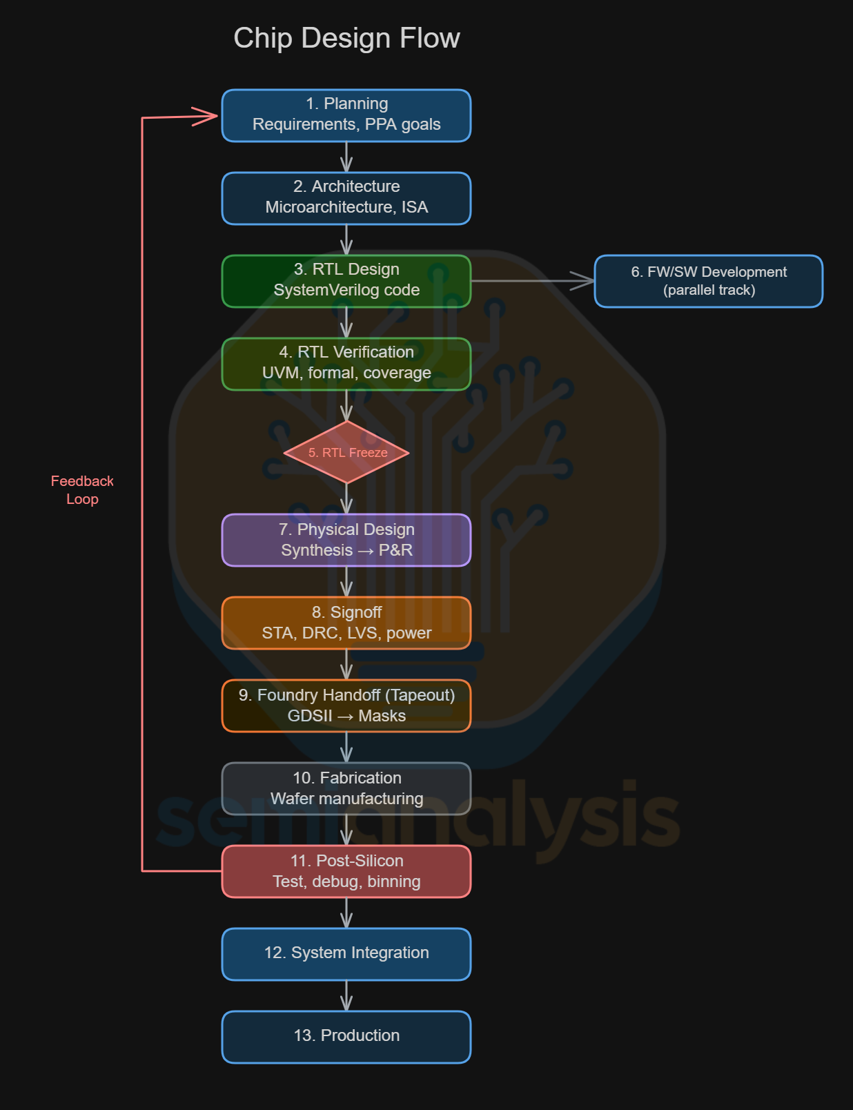
Planning: Define the product requirements, target market, and PPA (power, performance, area) goals that will constrain every decision downstream.
Architecture: Design the microarchitecture: instruction set choices, cache hierarchies, bus widths, and the block diagrams that partition the chip into manageable units.
RTL Design: Write the actual hardware description code, almost always in SystemVerilog, that specifies every register, mux, and state machine in the design.
RTL Verification: Exhaustively test or prove that the RTL behaves correctly across billions of scenarios. Implemented with Testbenches or formal proofs.
RTL Freeze: The design is locked. No more functional changes allowed, only bug fixes that pass a strict change control review.
FW/SW Development (Parallel): Firmware and software teams begin bring-up on emulators and FPGA prototypes, often running in parallel with physical design to save months of schedule.
Physical Design: Logic Synthesis to convert the RTL into a gate-level netlist, Placement (gates onto the die), routing (wiring them together) and floorplanning (assigning areas of the die for each functional block).
Signoff: Run final checks that the design meets timing closure (every signal arrives on time), power budgets, and DRC/LVS (manufacturing rule) requirements.
Foundry Handoff: The finished layout is exported as a GDSII file, the multi-gigabyte blueprint the foundry uses to create photolithography masks. Known as the “tapeout” milestone.
Fabrication: Wafers are manufactured in the fab over 3-4 months, passing through thousands of processing steps across dozens of tools.
Post-Silicon Validation: Real chips come back from the fab. Post-silicon bring up engineers test them on custom boards and probe cards, debug errata, and decide on binning strategies (productizing parts with varying yield and performance into different SKUs). Multiple steppings may be done in this phase. Reliability tests are done with burn-in and Final Test.
System Integration: Validated chips are integrated into boards, packages and connected to devices, with drivers, BIOS, and OS support qualified with System Level Testing.
Production: Volume manufacturing ramps to meet demand, with ongoing yield optimization and supply chain coordination.
This is a simplified “waterfall” view. In practice, many of these stages overlap heavily and iterate. Architecture bugs found during verification force RTL changes; timing failures in physical design send engineers back to re-optimize critical paths. A modern SoC program manages dozens of these feedback loops simultaneously, which is exactly why EDA tooling exists, no human team could track it all by hand.
1. Planning
The first stage to any chip is to decide on what role the chip serves. Each design department usually specializes in a given family of chips, be it CPUs and accelerators to the more mundane system controllers and embedded sensors. The product requirements and high level specifications are defined with respect to the current generation of products in the market, along with competitive analysis of others in the target market.
Strawman concepts are proposed that evolve rapidly as Program Managers work within the insertion schedules of various IP blocks from the design teams that may be ready for integration. Learnings from Post-Mortems of previous projects are factored in, forming a knowledge base to work from on what works and what is too ambitious for a given timeframe.
The key high-level metrics here are PPACt: Performance and Power consumption, usually given as a percentage improvement over the prior generation and where it might sit in the competitive landscape, the area that such a design takes up in silicon on a given process node, which translates to Cost. Time to Market is the final metric that determines whether the product is viable both from a design time and product competitiveness standpoint. In a fast growing market where performance doubles every few years, being 1 year late could spell the end of a project’s success.
These feasibility studies will then need to be greenlit by management before project kickoff begins in earnest. Each company has to work within their R&D budget with finite engineering resources. Scheduling resource allocation with ongoing projects in the roadmap requires strict completion deadlines so engineers can be released to start working on the next project. Communicating early with suppliers to project the wafer, memory and packaging demands for each design is now increasingly important to secure capacity.
2. Architecture Layout
Closely tied to planning, the architectural layout is done alongside design space exploration. A high-level floorplan diagram sets the initial area bounding boxes for each logic and I/O block design team to work within. Each functional block is broken down into smaller elements that are easier to design and can be repeated multiple times across the design. These area budgets may increase over the design cycle based on features that may be added later that take more area. For example, a feature update in an Instruction Set Architecture (ISA) with additional computing elements to support new instructions. On the AI accelerator side, this equates to adding dataflow accelerators and doubling Matrix Multiplication engine widths.
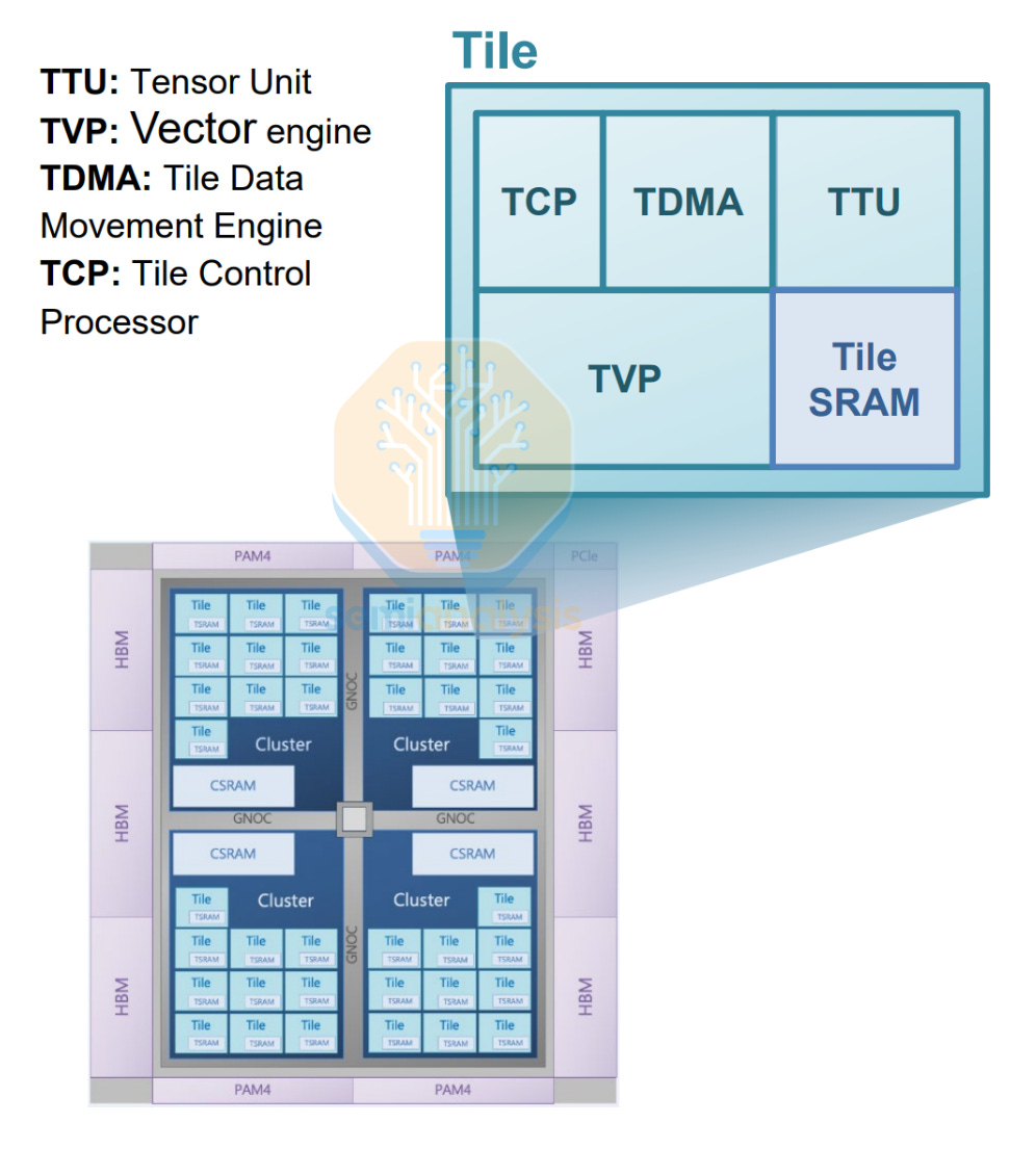
Block diagrams are drawn up with relations and Network on Chip (NoC) bandwidth requirements decided for each functional block, with memory bus widths and SRAM area budgeted based on cache hierarchy and early simulations of performance vs memory pressure. These simulations, known as Design Space Exploration, have traditionally been done with targeted Design of Experiments that simulate the performance impacts and interactions between each functional block, varying unit sizes, widths and bandwidths to find the lowest hanging fruit to maximize performance gains.
Going forward, this step has increasingly been accelerated with AI, as the task is easily verifiable with assignable reward functions for PPA in a multi-dimensional input space. First party AI-driven exploration tools such as Synopsys’ DSO.ai have followed the many internal efforts by the fabless design houses to leverage AI to accelerate pathfinding and planning decisions. An in-depth analysis on this will be featured in Part 3 of this EDA series.
3. RTL Design
With the architecture specified, engineers must then describe exactly what the chip does. This is done at the level of registers, data paths and combinational logic, which will later be translated into transistor implementations. This description is called RTL (Register Transfer Level) code, and it is where the design’s behavior is defined in a language that both humans and synthesis tools can read. Most of the engineering hours in the chip design flow is spent writing and verifying the RTL code. Below we look at the aspects to RTL design.
Signal Timing
In the real world, transistors don’t switch instantaneously. There is a propagation delay where it takes some time for an input change to produce a stable output. This delay has two components: the gate delay (how fast the transistors themselves switch) and the wire delay (how long the electrical signal takes to travel along the metal interconnect to the next gate). At advanced process nodes, wire delay ends up dominating gate delay as transistors switch faster while datapaths lengthen with complex designs.
Digital chips use a clock signal to synchronize all operations. Two timing constraints govern correctness. Setup time requires that input data be stable for a minimum period before the clock edge arrives. Hold time requires that data remain stable for a minimum period after the clock edge. The clock period (the inverse of frequency) must be long enough to accommodate the slowest signal path in the entire design. This worst-case path is called the critical path. If your critical path takes 0.2 nanoseconds and you want a 5 GHz clock (0.2 ns period), you are right at the edge, with no margin for process variability. This is why timing optimization consumes enormous effort in chip design, with many trade-offs in performance and complexity.
State Elements
Combinational logic computes outputs from inputs, but it needs to be combined with memory to build useful functions such as a counter, a processor pipeline stage, or a protocol engine. These memory registers are implemented as flip-flops. A flip-flop captures and holds one bit of data on each clock edge, acting as a tiny one-bit memory. Multiple flip-flops are chained together with combinational logic to form a Finite State Machine (FSM). This circuit steps through a defined sequence of states, one clock cycle at a time. This is sequential logic, which forms the base for chips to compute. Thus, RTL is an abstraction that describes how data moves between registers and combinational logic on each clock cycle.
Writing the RTL
RTL is written in a hardware description language (HDL). The dominant choice today is SystemVerilog, an extension of the original Verilog language that adds features for both design and verification. VHDL, the older alternative, still appears in aerospace and legacy applications. A designer writing RTL specifies what happens on every clock edge, where data moves between registers, arithmetic operations execute, and state machines transition. Synthesis tools (covered in the next section) then convert this description into actual gates and transistors.
Once written, RTL passes through linting, a static analysis that catches coding mistakes, race conditions, and syntax errors. This is done as a quick code review without requiring simulation. VC SpyGlass from Synopsys is the industry-standard linting tool, flagging seemingly subtle issues that could cause intermittent silicon failures. This is essentially the chip design equivalent of a compiler’s warning flags, just with far costlier consequences.
IP Integration
In most modern SoC (System on Chip) designs, only about 20-30% of the RTL is truly custom logic designed in-house. It is easier to reuse previous designs for non-critical components, with the rest comprised of licensed IP blocks. These are pre-designed, pre-verified modules purchased from third-party vendors. ARM provides processor cores, GPU and other IP. Synopsys DesignWare supplies USB, PCIe, DDR memory controllers, and hundreds of other interface blocks. Broadcom’s excellent high speed IO can be used if they are handling the rest of your chip design. Meanwhile, smaller IP vendors sell everything from GPIO interfaces to cryptographic accelerators.
IP licensing is the result of economics. Designing a custom PCIe Gen 6 controller from scratch would require spinning up a dedicated team of I/O design and verification engineers working to prove compliance with PCI-SIG’s specification. Licensing one costs a fraction of that and comes pre-verified against the spec. However, the IP integration itself can be challenging, something we will cover for our subscribers below.
4. RTL Verification
The RTL code then goes through the verification process, crucial to iron out any bugs or design errors within. This is done through simulation, which runs the design in software, applying stimulus, and checking the outputs. Three commercial simulators dominate the market, in order of ubiquity:
VCS (Synopsys): The market leader, known for raw simulation speed and deep integration with the rest of the Synopsys flow.
Xcelium (Cadence): Cadence’s simulator, competitive on multi-core performance and mixed-signal simulation.
Questa (Siemens EDA): Strong in advanced debug and coverage analysis, with deep UVM support.
Most large chip companies license at least two of these. Running a full regression suite with tens of thousands of test cases on a complex SoC can consume thousands of CPU core-hours per run. Dedicated on-prem verification servers are usually insufficient these days, with cloud-based simulation on AWS and Azure shoring up short-term demand as teams try to burst capacity during crunch periods before tapeout. The amount of data this generates is also staggering, with multiple Petabytes of disk space required to house just a single chip’s entire definition and test items.
As mentioned above, you will usually find more Verification engineers than any other single role in a chip design house. With chips getting more complex, even more things need to be verified with one another, placing huge demands on the verification staff. We will dive into what this means for chip design in reality for our subscribers below.
The Verification flow takes two paths: Standard DV testing on one end, and Formal Verification with proofs on the other.
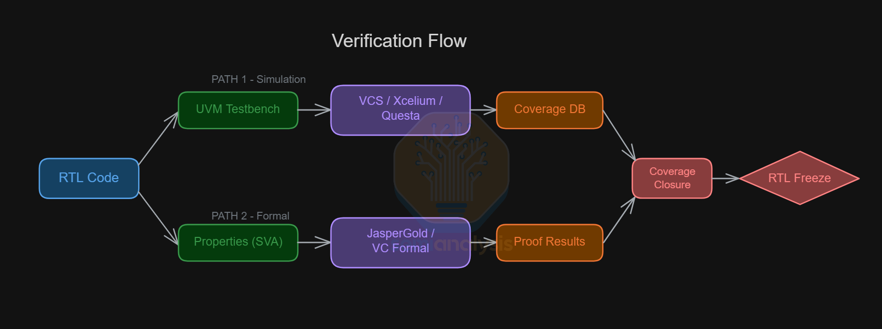
UVM Testbench
RTL simulation is structured in UVM (Universal Verification Methodology). This is an industry standard SystemVerilog library and method for building reusable testbenches. Before UVM was standardized by Accellera in 2011, every team rolled their own testbench architecture. UVM brought the industry together by defining a common set of components:
Sequencer: Generates sequences of transactions and feeds them to the driver. This is where test scenarios are defined.
Driver: Converts abstract transactions (e.g. “send a 32-byte read request”) into wiggling signals on the design’s input pins.
Monitor: Passively observes signals on the design’s interfaces and reconstructs the transactions that occurred.
Scoreboard: Compares expected outputs from a reference model against actual outputs from the design. Any mismatch is flagged as a bug.
The testbench is used for constrained random verification. Instead of hand-writing every test case for directed testing, the engineer defines constraints such as legal address ranges, valid packet formats and protocol rules. The tool then randomly generates millions of input combinations within those bounds. This approach finds corner-case bugs that might not be caught with directed testing. These constrained random regression tests are very resource intensive due to the large sample range, but is usually more effective for fault detection compared to writing directed tests.
Formal Verification
Formal verification takes a fundamentally different approach from simulation. Instead of applying specific inputs and checking outputs, formal tools use mathematical proof engines such as SAT solvers and model checkers to exhaustively prove that a design property holds for all possible inputs and all possible sequences of states. If the property can be violated, the tool produces a concrete counterexample showing exactly how. FV is done with properties, usually SystemVerilog Assertions (SVA) that define the expected behavior.
The leading tools are JasperGold (Cadence) and VC Formal (Synopsys). Formal verification shines for protocol compliance (e.g. the handshake signal is never asserted for more than 3 cycles), control logic correctness, and security properties (e.g. this register is reserved for software with elevated privileges). However, FV’s limitation is scalability. Formal engines hit capacity limits on datapath-heavy designs with wide buses. In practice, formal and simulation are complementary. FV proves critical properties exhaustively on targeted blocks, while simulation covers the full chip at statistical confidence.
5. RTL Freeze
To know when verification is complete, engineers look at several coverage metrics, a quantitative measure of what each testbench has exercised. There are two categories:
Code coverage measures structural completeness:
Line coverage: Has every line of RTL been executed?
Branch coverage: Has every possible branch been taken?
Toggle coverage: Has every signal been toggled between 0 and 1?
FSM coverage: Has every state and transition in every FSM been visited?
Functional coverage measures intent:
Did we actually test the scenarios we care about?
Are there known corner cases that need to be focused on? (for example: concurrent writes to the same address, FIFO buffer is full while interrupt pending)
What are the specific variables to sample to test these scenarios? Covergroups are defined in SystemVerilog that contain explicit descriptions of these test cases, and tracks if a regression test hits specific variables.
Coverage closure is the final step in the verification process. While 90% of test cases coplete quickly, ironing out the remaining 10% with functional coverage takes serious effort, sometimes requiring weeks to write targeted tests while adding or modifying constraints and exclusions in other tests. The more specific and complex a test case is, the more esoteric the knowledge is in whether a design might be susceptible. Design houses tap on their vast history of learnings from previous designs to help inform and prioritize the most important tests.
When all coverage goals are met and no open bugs remain at the target severity level, the project’s RTL is frozen. This formal milestone, known as RTL Freeze, signals that no more functional changes to the RTL are permitted. From this point forward, any modification must go through a formal process known as Engineering Change Order (ECO), requiring re-verification and equivalence checking. ECOs may be required in the design process at a late stage to fix a bug or tweak timings that were not caught earlier. RTL Freeze ensures that the next step, Physical Design, has a concrete base to work from, separating front-end design from back-end physical implementation.
While verification is often overlooked as the unglamorous side of chip design, it is critical to the development of new architectures. Designing a chip is easy. Knowing your design works with all possible scenarios is hard.
6. Firmware / Software Development
With the chip development process already taking years, software teams cannot afford to wait for silicon to arrive before beginning to write software for it. An operating system, firmware stack, and driver suite need to be substantially ready before the first chip comes back from the fab. To write software concurrently with hardware development, engineers rely on Pre-Silicon Hardware Emulation. The chip’s RTL design is mapped onto large arrays of FPGAs that execute the chips functions at 50MHz speeds. Programmable logic elements in the FPGAs are routed to roughly match the logical configuration of each design, enabling these emulators to run 1000x faster than pure software RTL simulation on a CPU.
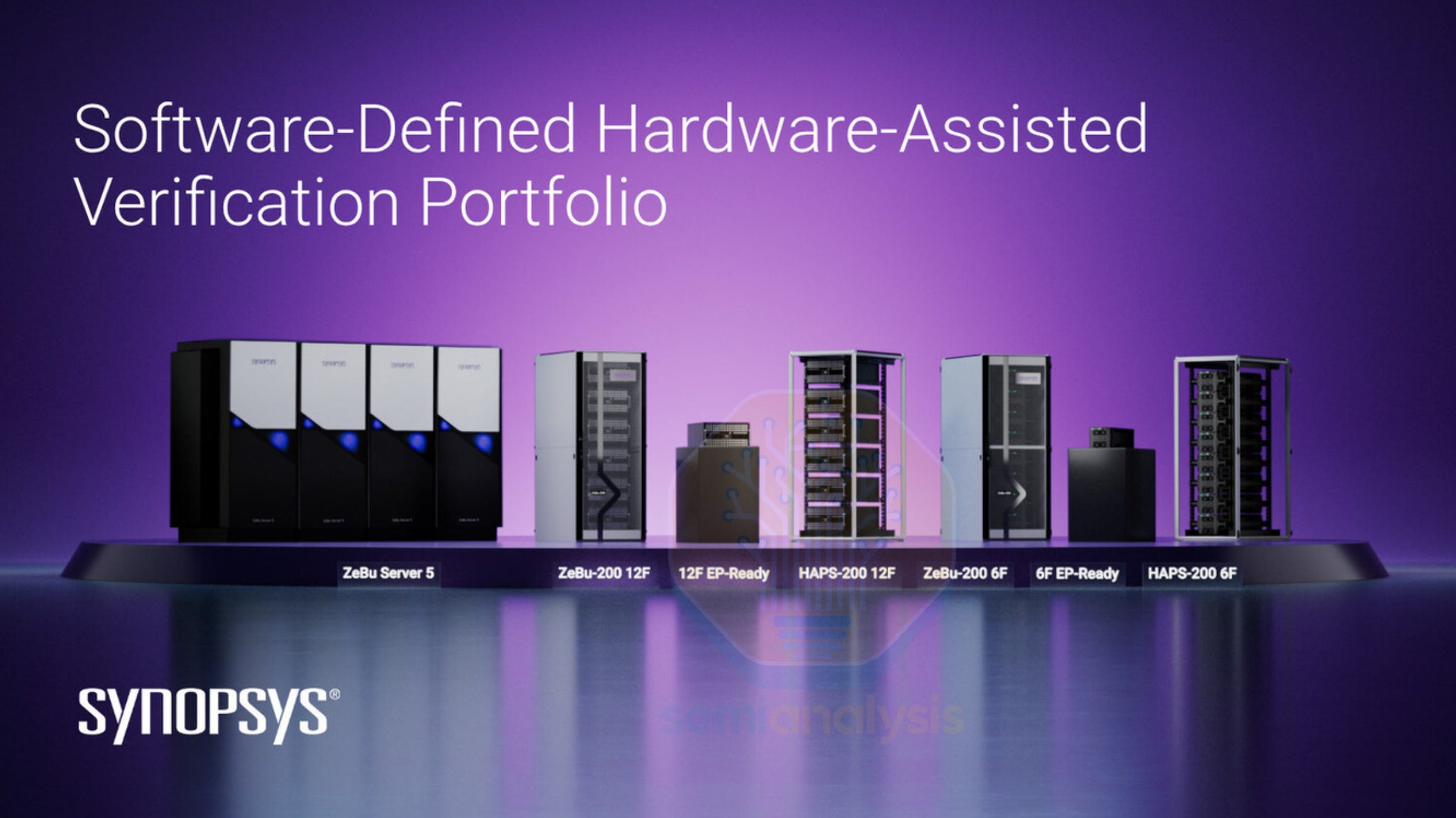
The two dominant platforms are ZeBu from Synopsys and Palladium by Cadence. Synopsys’s latest ZeBu-200 clusters can emulate up to 23 billion gates and delivers up to 2x the runtime performance of its predecessor. Cadence’s Palladium Z3 can scale to design with up to 48 billion gates and is 1.5x faster than the Z2 generation. These systems allow firmware teams to boot Linux, test firmware, and conduct software validation months before silicon arrives.
7. Physical Design
Up to this point, the chip exists only in high-level RTL descriptions. Before Physical Design can take place, a crucial translation step must be done.
Logic Synthesis
Logic synthesis transforms RTL code into a gate-level netlist, a connectivity map of logic gates drawn from a foundry’s standard cell library. These synthesis tools parse the RTL code and determines the right combination of logic gates, connected in a certain order, to carry out the functions described by RTL. We will explain what these logic gates are below.
On top of this, the synthesizer optimizes the netlist and works within the limits set by the design. It balances timing (can the gates in this circuit complete the operation within 4 clock cycles?), area (how many gates can I squeeze into the area set out by the architectural description?), and power (how many watts worth of power loss from the dynamic and static leakage of these logic gates?). These conflicting goals are somewhat mitigated by techniques such as minimizing repeated logic, sharing logic gates across multiple functions and retiming functions to reduce the load on critical paths. The tool explores thousands of alternative implementations to find the best tradeoff between these demands.
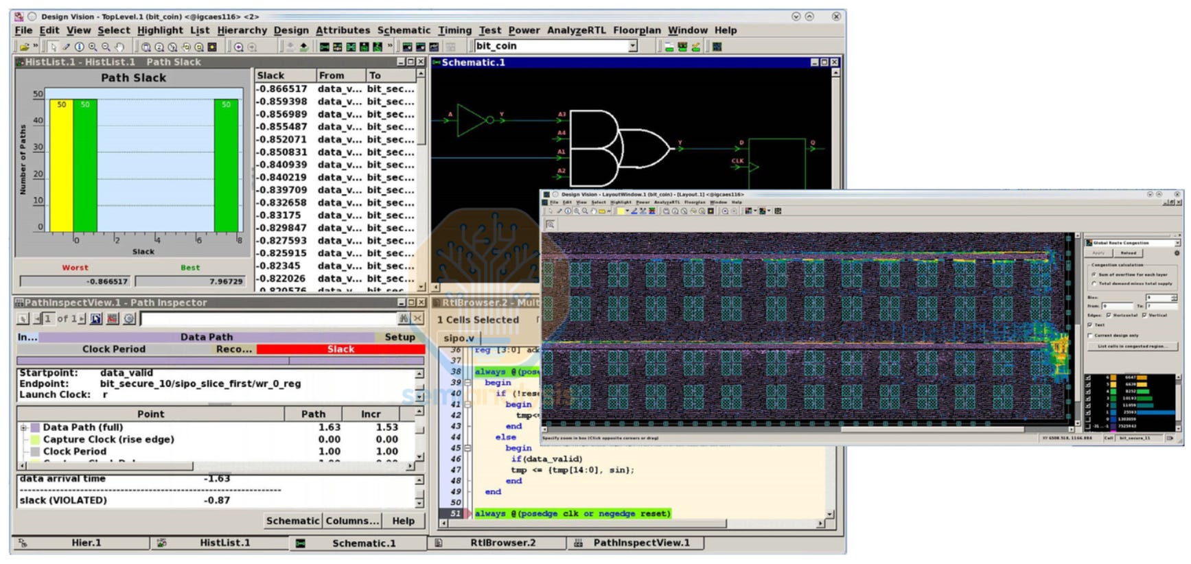
The original and still dominant tool is Design Compiler from Synopsys, which established the entire category with multiple versions such as NXT and Ultra with greater integration and features Design Vision, a graphical interface for engineers to evaluate the synthesis flow. Cadence offers Genus as their synthesizer. Synopsys now pushes Fusion Compiler, which unifies synthesis with place and route in a unified flow to allow cross-probing between RTL, timing and layout. We cover these Unified EDA flows in more detail below.
Equivalence Checking
Once RTL has been synthesized into a gate-level netlist, you have to check that the synthesis tool did not introduce any bugs. To do this, the design is proven mathematically with Equivalence Checking, a formal technique that verifies two representations of a design (RTL and gate netlist) are functionally identical, input for input, output for output. Formality (Synopsys) and Conformal LEC (Cadence) are the standard tools.
Equivalence checking is run at every major translation step, not just after synthesis. Later gate-to-gate transformations such as clock tree insertion, scan chain stitching, routing optimization, and after every ECO. With each transformation comes a potential vector to introduce errors. Equivalence checking is thus the safety net that catches errors introduced by the tools themselves.
Logic Gates
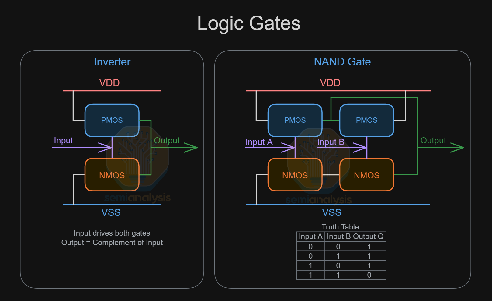
The synthesizer selects from a range of logic gates in a standard cell library, with each logic gate carrying out a Boolean function, translating a given set of binary inputs into an output. The permutations between inputs and outputs are listed in Truth Tables as shown above. The seven basic logic gates are INV and NAND as shown above, AND, OR, NOR, XOR and XNOR. Transistors laid out in standard cells then carry out these operations in the real world, with the output signal voltage pulled up to Vdd for “1” or pulled down to Vss for “0”.
Standard Cell Libraries
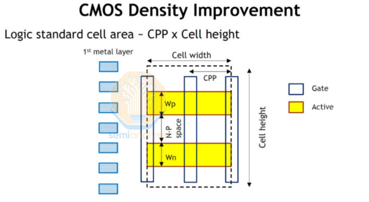
The above gates are not designed from scratch. Instead, layouts are pulled from a standard cell library, a catalog of pre-designed, pre-characterized logic building blocks provided by the foundry or a third-party IP vendor that obeys all design rules. Each cell has a fixed height and a variable width, tiling neatly in horizontal rows across the die like bricks in a wall. This standardized, ordered layout with two sites for transistors (usually PMOS above NMOS) and standard pitches for power delivery is crucial to enable automated place and route.
Apart from the basic logic gates above, more complex standard cells are offered with advanced functionality. These combine logical operations into a higher level function that will be used repeatedly throughout a design. Those who work closely with the foundry may also design their own custom standard cells for these complex operations. Examples include (in increasing complexity), AOI, OAI, Registers, Multiplexers, D-Flip Flops and Full Adders. Special purpose cells are also featured throughout the design that deal with functions beyond logical computation. Examples include IO pad cells, Tap cells, Filler and Decap cells, Tie-high and Tie-low cells, power and clock gate cells and level shifters to carry signals over multiple voltage domains. SRAM Macro compilers are also included in each node that generates Static RAM blocks which are the densest memory cells in a logic process.
A modern standard cell library for an advanced node like TSMC N2 contains tens of thousands of individual cells. Each logic gate will have multiple layout options to choose from depending on wire routing and signal pin accessibility. Each gate will also come in several drive strength options, where higher drive strength cells are used when its output needs to drive multiple input signals. These are used selectively as higher drive current transistors have greater leakage power. Modern TSMC process nodes have upwards of 6 Threshold Voltage options to enable fine tuning of signal reliability and power. One of the problems with Intel’s initial 18A was that there were only 4 VT options (Intel only used 3) vs 6 at TSMC meaning even if Intel performs better at a given point, the design has a harder time being on the pareto optimal curve across all VTs. Intel’s 18AP fixes this.
Synthesis tools pick the right size for each cell based on timing and power constraints. With millions of permutations to choose from, EDA tools in both Synthesis and Physical Design are mandatory to navigate this optimization problem.
With Moore’s law slowing, newer nodes with novel area scaling techniques have exacerbated the layout complexity further. TSMC’s N3 FinFlex and N2 NanoFlex mix standard cells of different cell heights together, adding another layer of design constraints. Multiple library options are also offered for each node, such as HD high density and HP High Performance with different standard cell dimensions and power characteristics. For Gate All Around processes (SF3, 18A, N2), multiple nanosheet width options are available for each standard cell height. Designers can mix and match different libraries for each region of a chip to extract the best PPA from the new process. Apple for example uses TSMC’s 3-2 FinFlex for its high performance CPU cores, with the rest of the die adopting the much denser and lower power 2-1 FinFlex library.
The standard cell library is the foundry’s main commercial interface with chip designers. It encodes not just logic functions but the foundry’s manufacturing capabilities, design rules, and process characteristics into a form that EDA tools can consume. When a fabless company “ports” a design to a new foundry, migrating the standard cell library is the first and most impactful step, and the one that triggers the most re-work across the entire tool flow.
Process Corners
Physical Design tools must also account for the effects of the real world, namely on variability in manufacturing. A cell’s speed and power consumption may shift significantly depending on variations in Process, Voltage and Temperature (PVT). Libraries are therefore characterized across a range of PVT corners as shown below.
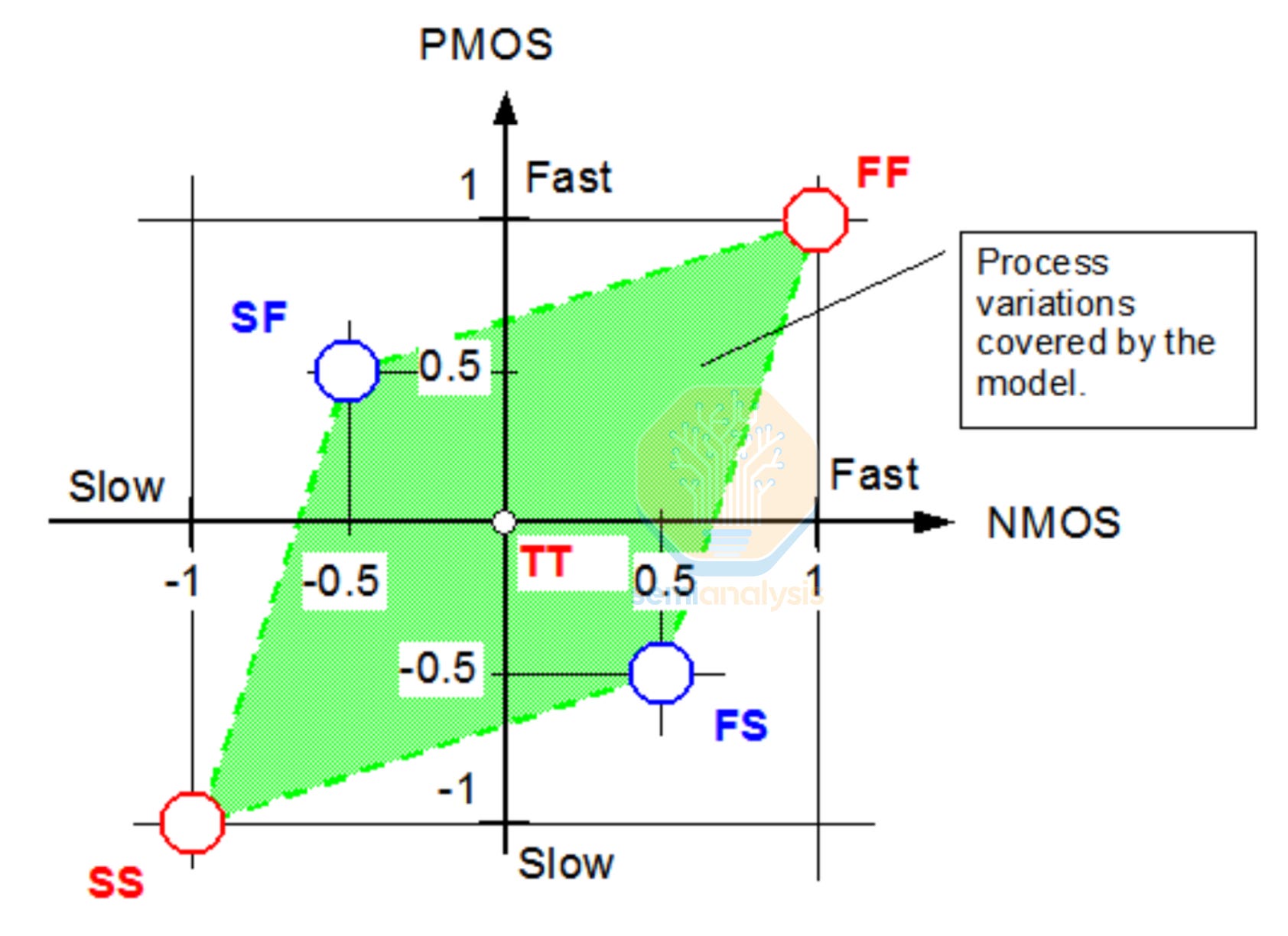
TT (typical-typical) is the nominal case. FF (fast-fast) means both NMOS and PMOS transistors came out faster than nominal. SS (slow-slow) means both came out slower. FS and SF capture skew between NMOS and PMOS. These cases are particularly tricky because they affect circuit balance in ways that symmetric corners do not.
Voltage is varied around the nominal supply. For example, 0.75 V nominal with corners at 0.675 V (-10%) and 0.825 V (+10%). Lower voltage means slower switching and at lower power. Temperature ranges depend on the application. Consumer chips might cover 0°C to 105°C, while automotive-grade libraries must be characterized from -40°C to 125°C. Designs must meet timing at the slow corner and stay within its power budget at the leaky corner.
Metal Interconnect
Standard cells define the active transistor layer at the bottom of the metal interconnect. The lowest metals, M0 and M1, are used within cells to connect transistors to pins. These are thin, high-resistance wires, fine for short distances inside a cell but not for routing signals across the die. Each alternating metal layer has lines that are perpendicular in orientation, with odd layers for north-south routing and even layers for east-west routing.
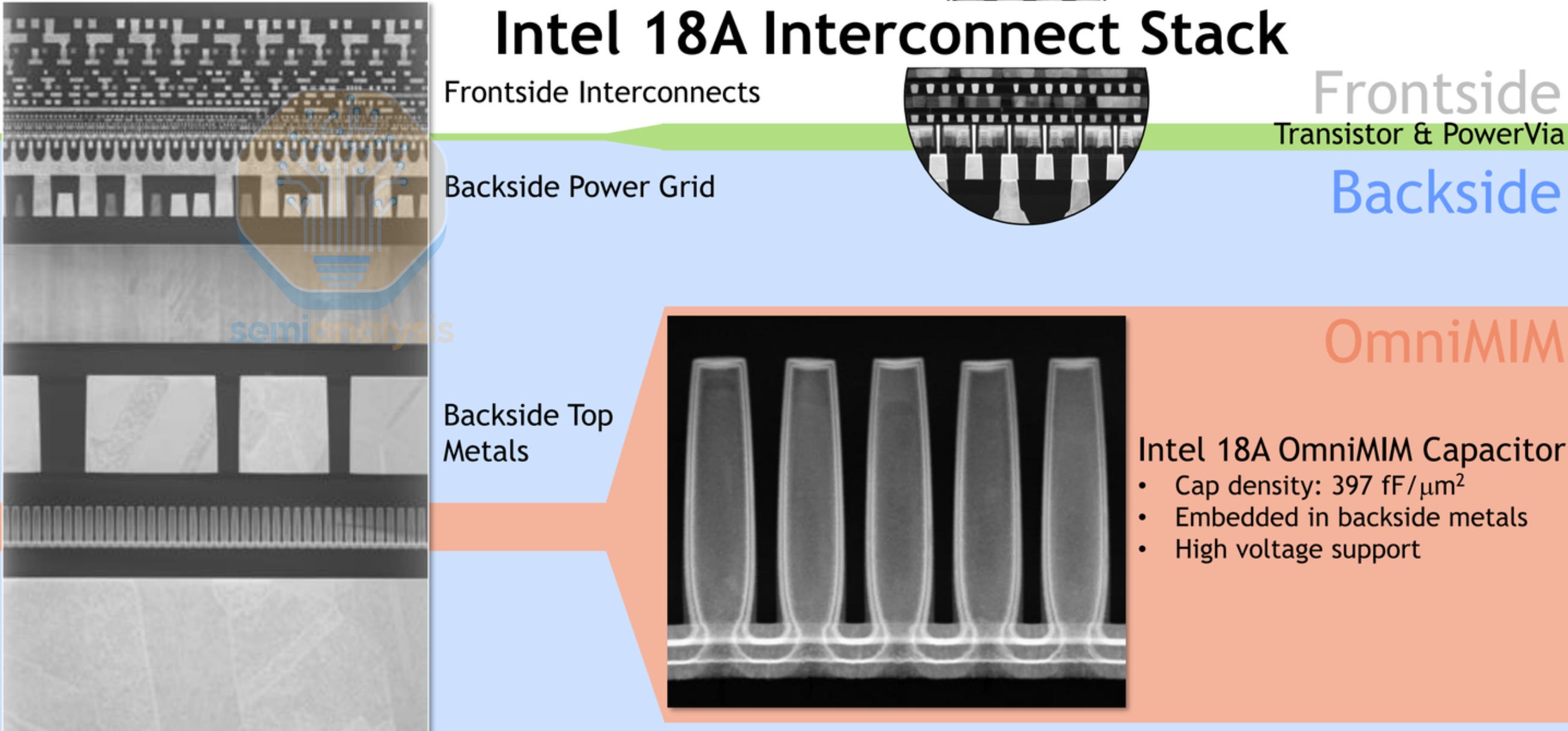
Semi-global metals (M3 through M5) handle block-level routing, connecting standard cells to each other within a functional unit. These are progressively thicker and wider, reducing resistance for longer runs. The thickest top metals above are reserved for the power distribution network and global clock trees. The total number of metal layers depends on the complexity of the chip, from 10 layers in the low-cost mobile SoC to 19 layers in a high performance AI processor. Backside Power Delivery schemes such as Intel’s 18A above unlock another dimension for routing tools to utilize by segregating power and signal lines, reducing parasitic capacitance and signal interference.
Process Design Kit
All of the parameters above are detailed and provided by the foundry in a Process Design Kit (PDK). This dense package of files, models, and rules translates a foundry’s manufacturing process into terms that EDA tools can understand.
Each PDK comes with the following information, each having their own industry standard file formats:
The LEF file (Library Exchange Format) provides the physical description of the standard cells, including pin locations, metal blockages (areas to avoid) and the cell boundary. Place and route tools use LEF as it contains sufficient geometry to position cells and connect wires.
LIB files (Liberty Format) contain timing arcs, defining how long a signal takes to propagate and decay, power consumption tables, and noise immunity data. Separate .lib files are made for each PVT corner combination.
SPICE models (Simulation Program with Integrated Circuit Emphasis) capture detailed analog behavior of the transistors such as threshold voltages, leakage currents, capacitances, and how they shift across process corners. Other simulation models of passive devices such as resistors, inductors and capacitors may be included.
Parameterized cells (P-cells) are used in the analog I/O regions, generating transistor dimensions based on certain variables that the designer can adjust. This is vastly more efficient than drawing out every cell for each variable dimension.
Parasitic extraction decks tell extraction tools how to calculate the resistance and capacitance of every wire and via in the layout. These come in multiple corners, RC-max (worst-case slow interconnect) and RC-min (best-case fast interconnect) to account for manufacturing variation.
The Design Rule Manual (DRM) contains thousands of geometric constraints such as minimum spacing, minimum width, enclosure rules, blockage and density requirements. Physical Verification parameters and provided, detailed in the next section.
GDS (GDSII Stream) layout parameters may also be provided, giving an example of the full, exact physical layout for every transistor and metal layer, including diffusion regions, polysilicon gates, contacts, and vias. This file is what ultimately goes to the foundry for tapeout.
A standard cell as seen in a GDS viewer. Each color represents a different fabrication layer. Polysilicon gate (red), metal interconnect (blue), and vertical contacts/vias between layers (blue squares).
PDK Versions
As the process is being developed, customers begin to design test chips and learn about the process characteristics. As such, PDKs go through many revisions on its way to version 1.0 for production tapeouts. The major PDK milestone releases are:
PDK 0.1 / PDK 0.3: Built entirely from TCAD simulation (Technology Computer-Aided Design), not real silicon data. Used for early architecture exploration and pathfinding with wide uncertainty bands. Only available to anchor customers under a Joint Development Agreement (JDA), up to 2 years before volume production. Standard cell dimensions are defined but libraries at this stage are minimal.
PDK 0.5: Incorporates early silicon test data from short-loop wafers and initial test chips. This is where real chip design typically begins, starting with test chips. Models are substantially refined, but PVT corner coverage is still incomplete. Data for process corners will be available, but not full silicon models. The standard cell library is growing but not finalized. Regular foundry customers gain access at this stage.
PDK 0.9: Provides full silicon characterization across all PVT corners. Near-final Physical Verification decks are prepared, validated against millions of test structures. All major EDA tool vendors will have broad support and have IP available.
PDK 1.0: The final production-ready package. Complete standard cell libraries with all Vt variants and circuit models are available. This is what production tapeouts use. PDK 1.0 is a foundry milestone that signals manufacturing readiness.
Between each major version, the foundry issues point releases that tighten design rules, narrows model uncertainty and adds DFM (Design for Manufacturability) hotspot rules discovered from real fabrication data.
PDK Licensing and Access
Foundry PDKs are universally NDA-protected, and access is controlled through a rigid tiered system that reflects both business relationships and IP security.
Tier 1: Anchor / JDA customers (eg Apple for Mobile, AMD / Nvidia for HPC). These companies are heavily involved with process technology definition and co-development, receiving access 3+ years before production. They push the design rules and may “bankroll” the foundry to develop specific process features. In return, they get first-mover advantage and the deepest collaboration.
Tier 2: EDA and IP partners. Synopsys, Cadence, Siemens EDA, and IP vendors like Arm receive early PDK access for tool validation and IP development. Their standard cell libraries, memory compilers, and interface IP must be qualified and available for fabless design houses to use, requiring several months of engineering lead time to implement.
Tier 3: Standard foundry customers. These companies design chips on an established process but do not influence its development. They accept the design rules as-is.
Tier 4: Academic and research. Heavily restricted. Universities may receive limited PDK subsets for research, and usually many years after the process has matured.
Even then, Tier 1 customers never see the foundry’s physical recipe. Chip designers see electrical characteristics, with no need to know the exact doping profiles, process temperatures, or etch chemistries. The PDK is an abstraction layer that makes the fabless model possible, protecting IP between foundry and customer.
PDK Timeline: Intel 18A
Sep 2022: PDK 0.3 now in hands of early design customers, test chips are under design for end of year tapeout.
Mar 2023: Shared the engineering release of PDK 0.5 (process design kit) with our lead customers and expect to have the final production release in the next few weeks.
Sep 2023: PDK 0.9 is “imminent” and many 18A test chips and shuttles for both internal and foundry customers are running in the fab.
Jul 2024: Intel released PDK 1.0 to foundry customers
Jan 2026: Launch of Intel internal Panther Lake CPUs on 18A
Open Source PDK
As foundry PDKs are closely guarded secrets, few will ever have the access to learn and use them. To date, only a few production PDK have been released as fully open source. In 2020, Google partnered with SkyWater Technology to release the SKY130 PDK, a complete, manufacturable design kit for SkyWater’s 130nm process. SKY130, originally developed by Cypress Semiconductor, includes SPICE models, DRC/LVS decks, standard cell libraries, and IO cells. Everything needed to go from RTL to fabricated silicon, published on GitHub under an Apache 2.0 license. GF180MCU and iHP130 are also open and similarly old or older.
While the technology is over 20 years old, it has been crucial for education and open source research as well as training open source models in Physical Design. The open-source EDA ecosystem includes OpenROAD for place-and-route and OpenLane for automated flow orchestration. Google has funded several multi-project wafer (MPW) shuttle runs, manufacturing community designed chips for free, enabling students to complete the entire RTL-to-GDSII flow without a single commercial license. Unfortunately Google pulled funding for these areas. Check out this link for more on this initiative.
Physical Design Tools and Functions
The two dominant physical design platforms are IC Compiler II (Synopsys) and Innovus (Cadence). Together, they handle virtually every advanced-node chip taped out today. The choice between them often comes down to which tool the team has the most expertise with. Decades of institutional knowledge built over dozens of projects make switching difficult and expensive. These tools take all of the parameters and considerations above along with the synthesized netlist and foundry PDK to generate a complete GDSII layout for tapeout. Engineers use these EDA tools for:
Floorplanning: Defines the chip’s physical outline and internal organization, akin to deciding the exact position of all walls and rooms in a house. Based off the high-level architectural planning above. Large macro blocks are placed (SRAM, PLLs, analog IP) and IO pin locations are demarcated along the chip perimeter.
Power Planning: The power distribution network (PDN) delivers supply voltage to every transistor on the chip. Horizontal and vertical power stripes with via stacks form a power grid mesh to feed power rails for transistors to access. The PDN must handle multiple voltage domains for power efficiency regions, along with the ability to selectively turn off power to regions when idling, a technique known as power gating. The goal is to minimize IR drop from wire resistance. Voltage supply must be uniform across the entire chip area, especially in dense power grid hotspots such as Floating Point units and Tensor Cores.
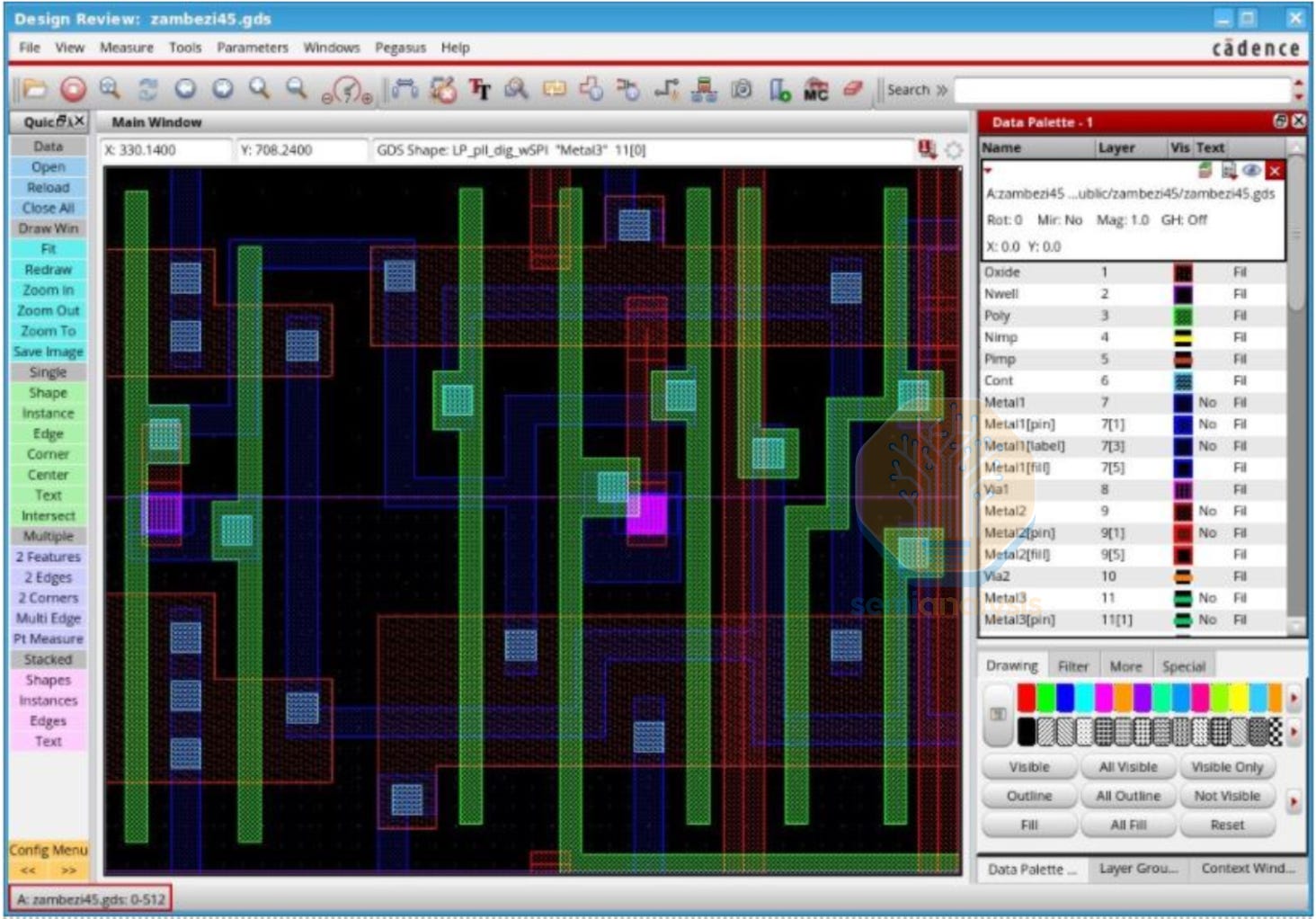
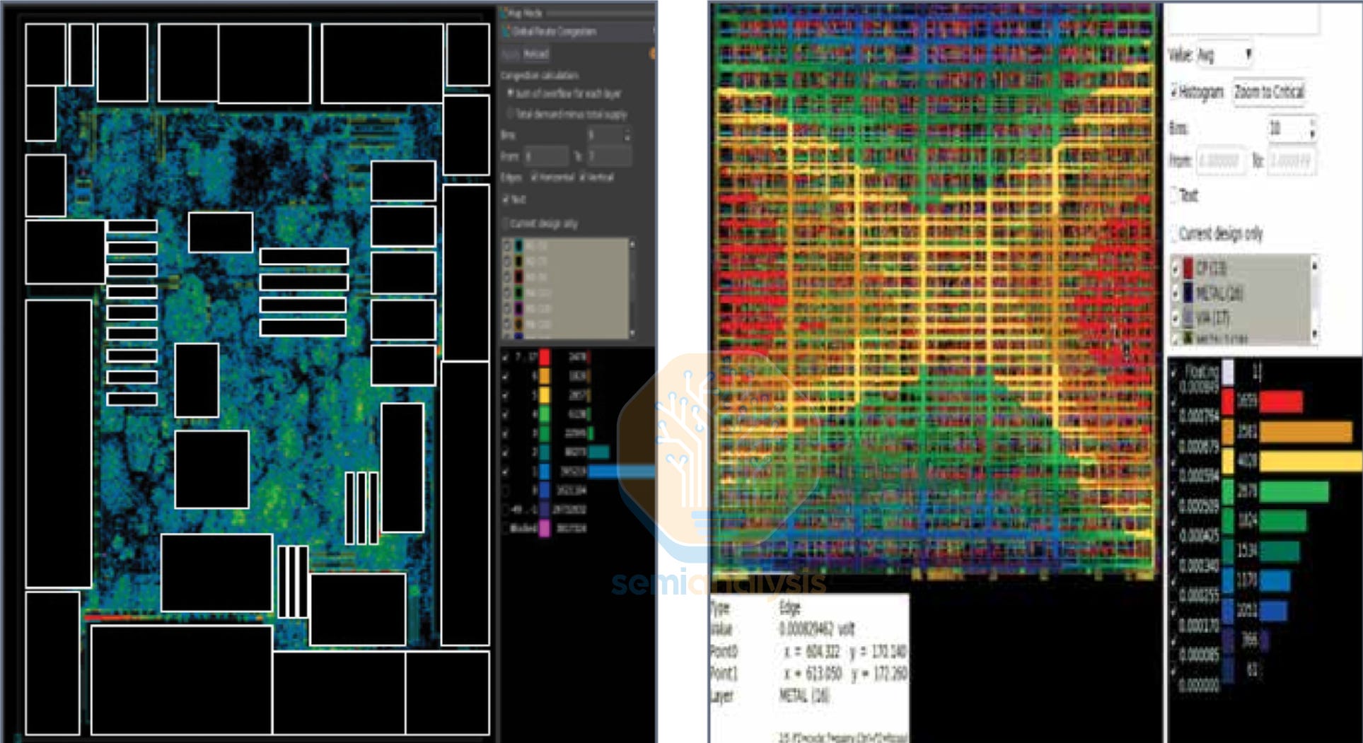
Placement: Assigns physical locations to millions of standard cells within the floorplan. Global placement optimizes total wirelength and minimizes congestion hotspots. Detailed placement then legalizes these positions, locking the standard cells into defined grid rows and resolving overlaps. Modern placers are timing-driven and congestion-aware, trading off wirelength for routability. The image above shows the cell density distribution in a design. Infrastructure cells are also added such as fillers, tap cells and spare cells reserved for ECO debugging.
Routing: Connects all placed cells to the metal interconnect stack above for both signal and power. Local, semi-global and global routing is handled by PnR tools to meet both power delivery and clock timing budgets. The tool will spread out standard cells and lower area utilization in locations with high routing congestion where cell pin density is too high for the metal stack to handle.
Clock Tree Synthesis: Builds the distribution network that delivers the clock signal from a central source to every transistor in the clock domain, ensuring synchronous operation. The goal here is minimizing skew, the difference in clock arrival times between any pair of functional units. Timing budget would be eaten up to account for variations in skew. Different blocks in a chip may operate in different clock domains for power efficiency regions, requiring clock domain crossings for signals to traverse between them.
Design for Test (DFT): Inserts testability structures into the physical implementation. Scan chains and DFT access pads are added with long shift registers so test equipment can load test patterns and retrieve results. MBIST (Memory Built-In Self Test) adds on-chip test logic for memory chips. ATPG (Automatic Test Pattern Generation) software computes the optimal set of input vectors for maximum test coverage.
Physical design is done over multiple optimization loops. After each major step, the tools run timing optimization, inserting buffers on long or high-fanout nets, resizing gates (swapping a standard cell for a larger or smaller variant), applying intentional skew (shifting clock arrival times to help critical paths), remapping logic (restructuring gate-level topology), and hold fixing (adding delay cells to prevent data from arriving too early). The tools iterate through these techniques to arrive at the best PPA.
8. Signoff
Much like RTL design and verification is locked in with RTL Freeze, Physical designs undergo Physical Verification (PV) before Signoff locks the GDSII in place. Signoff proves design will actually work in both function and manufacturability, across every operating condition and power scenario. Synopsys offers IC Validator, Cadence offers Pegasus, and Siemens has Calibre. All three have deep foundry entrenchment that are indispensable for the fabless design houses in properly utilizing a given foundry process. The main components to clear before Signoff are:
Design Rule Check (DRC): Verifies geometric constraints from the foundry. Minimum wire widths, spacings between shapes, imposed blockages and pattern density limits are obeyed. Advanced nodes impose thousands of such rules, with design rule manuals exceeding 1000 pages.
Layout vs. Schematic (LVS): Proves that the physical layout implements exactly the intended circuit connectivity, with no unintended shorts or opens. A netlist is extracted from the physical layout and compared to the original gate-level netlist to ensure logical correctness.
Electrical Rule Check (ERC): Catches floating nodes, shorted supplies and other electrical violations in the power grid. ERC checks for current density limits and ESD (electrostatic discharge) reliability.
Static Timing Analysis (STA): Verifies that every timing path in the design meets its setup and hold constraints. Tools like PrimeTime by Synopsys and Tempus from Cadence have more advanced functionality that look at timing across PVT corners and DVFS (Dynamic Voltage Frequency Scaling) curves, known as MCMM (Multi-Corner Multi-Mode) analysis.
Power Signoff: IR drop analysis verifies that the power distribution network delivers adequate voltage to every transistor under both static (average) and dynamic (switching) conditions. Wire currents are checked for electromigration limits, where electrons gradually move copper in the metal lines causing shorts and opens over time. Synopsys RedHawk-SC and Cadence Voltus tools handle power integrity verification.
Occasionally, ECO flows may have to be implemented to clear Signoff. A functional ECO fixes logic bugs by repurposing pre-placed spare cells, only requiring new masks in the lowest metal layer. A timing ECO, guided by PrimeTime, resizes or remaps cells to close timing, and may require a full mask set change. Each type trades flexibility for cost and turnaround time, the mechanics of which will be explained in the Steppings section below.
Unified Flows
Traditionally, each stage of the chip design flow operated as a silo. The RTL team wrote code and handed it to the synthesis team. Synthesis produced a netlist and handed it to place and route. They generated a layout and handed it to signoff. Each tool ran independently, creating a coordination nightmare when issues are found downstream that needed a fix from layout or even at RTL. These inevitable bugs would throw programs off by many weeks as these verticals are brought together to implement fixes. To address this, EDA vendors have unified the physical design process so every step is factored in concurrently rather than sequentially.
Synopsys Fusion Compiler was the first major answer to this problem. Built on a single data model, it unifies synthesis, place and route, and timing analysis into one engine. Cadence responded with iSpatial, which embeds the Innovus placement and optimization engines directly into the Genus synthesis tool. Unified flows bring the “Shift Left” philosophy. Have signoff-quality analysis earlier in the design process to avoid late surprises.
9. Tapeout
Once every signoff check passes, the design is exported as a GDSII or OASIS file, the industry standard formats describing the geometric shapes on every layer. This file is sent to the foundry, marking the milestone known as the tapeout, a term coined from the old days where GDSII files with sent on reels of magnetic tape. With this, the first mask set is designed. OPC (Optical Proximity Correction) algorithms modify the mask patterns with SRAFs (Sub-Resolution Assist Features) to compensate for optical distortion during lithography. Then mask making begins, followed by wafer fabrication.
10. Fabrication & Packaging
The fabrication process, from tapeout to first silicon arriving, typically takes 8-12 weeks. However, these first wafers can be expedited by purchasing Hot Lots, with higher priority wafer shuttles cutting down cycle times by several weeks. This allows post-silicon bring up engineers earlier access to begin debugging the new chip.
Before debugging can happen, silicon needs to be packaged to protect the fragile die and break out the tiny I/O bumps on the silicon surface to a reliable socketable package. On modern advanced processors, Heterogeneous Integration (chiplets) and Advanced Packaging come into play here. Multiple dies per package, 3D die stacking and 2.5D interposers such as TSMC’s CoWoS (Chip-on-Wafer-on-Substrate) technology are used to scale performance beyond the 26 x 33 mm reticle limit, the maximum die size that each lithography machine can expose.
11. Post-Silicon Validation & Bringup
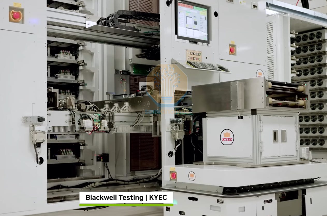
Automatic Test Equipment (ATE) from the likes of Teradyne and Advantest assesses every single chip coming off the production line, applying thousands of test vectors generated earlier by ATPG tools. JTAG debug interfaces within the chip provide direct access for post-silicon debugging of errata, when behavior deviates from expectations. Initial bringup features multiple rounds of testing, as more bugs are found and workarounds are implemented by updating the original firmware that was developed on FPGA emulators. In production runs, this step is known as Final Test (FT), where functionality is verified with tests that return a simple pass/fail result.
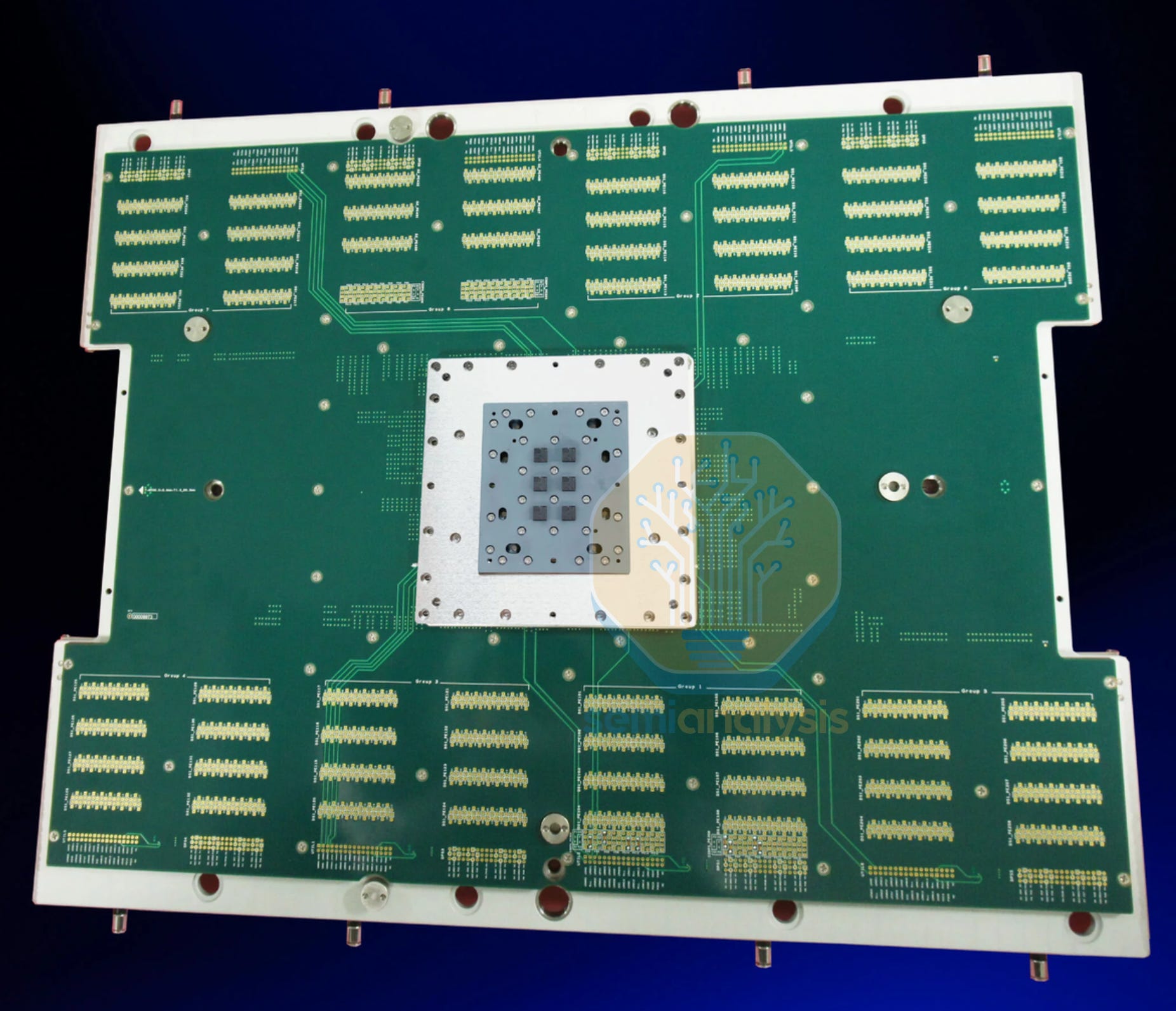
To access every single wire coming out of the package, large breakout boards known as Probe Cards are used. Bringup engineers use them to isolate each signal pin from the package, hooking up oscilloscopes to the terminals to measure signal integrity and strength that meets design requirements.
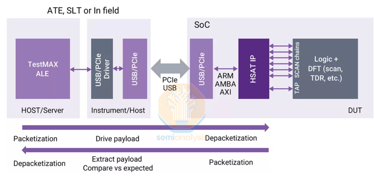
EDA vendors also have a hand in this space, with Synopsys TestMAX family of post-silicon testing tools providing comprehensive coverage from ATPG during the design phase, yield diagnosis, DFT structures that test patterns run on, and software to run and manage chip testing and results logging.
Burn-in Test
The next stage in the qualification process is for thermal reliability with High Temperature Operating Life (HTOL) testing. This is an accelerated burn-in where chips are tested beyond the typical operating temperature, weeding out any defective chips that may not survive the rated operating environment and thermal cycles over the expected lifetime of the chip. Removing these “infant mortality” class of chips greatly reduces the chance of customers receiving units that may fail early on in the Bathtub Curve of reliability.
Test durations depend on the reliability requirements of each design, though on average range from 72 to 168 hours. Reliability critical applications such as aerospace and automotive may undergo up to 1000 hours of stress testing. Lower end, cost sensitive consumer devices may only have some chips from each production batch randomly selected for extended testing. Testing requirements are standardized by JEDEC, with JESD47 covering HTOL and JESD22 for package reliability under high humidity and temperature cycling.
Steppings
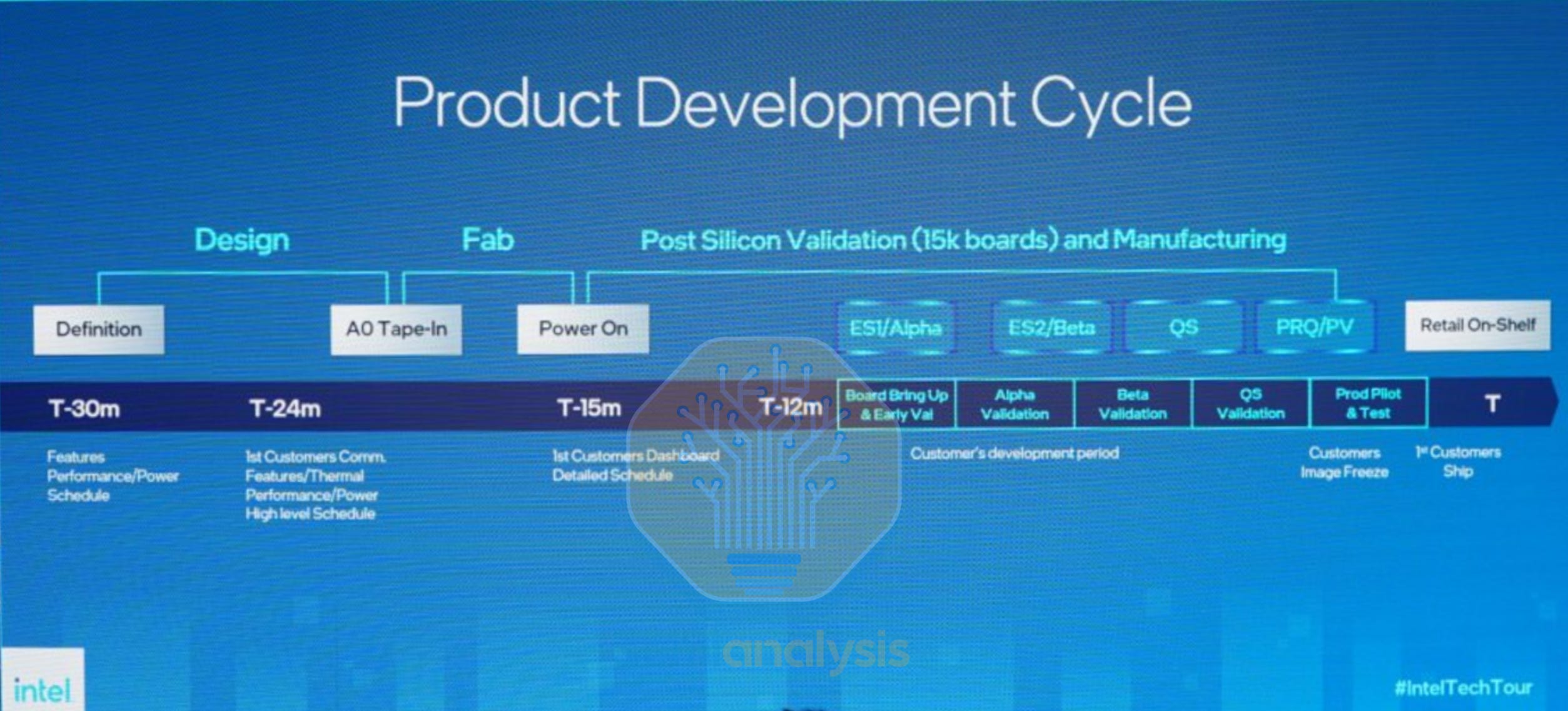
The first chip that comes back from the fab is known as A0 silicon. The ideal case is when A0 meets performance, power and reliability targets with no tweaks required for production silicon. However, sometimes the first chip doesn’t boot at all, and the fundamental flaw must be discovered. As such, most design teams budget additional development time to do multiple steppings, meaning the chip design is updated with new GDSII files sent to the fab for mask making and fabrication.
From Intel’s example above, multiple rounds of Engineering Sample (ES) versions are made, with a final Qualification Sample that is validated before production wafers are run. Steppings come with many codenames such as B1 or even E5 as was the case for the long delayed Intel Sapphire Rapids. Here’s a guide to what the stepping number means:
Major Stepping (A0 to B0): Requires full flow from DE to DV to PV, verification engineers have to create a new coverage closure, full mask set update usually required.
Minor Stepping (A0 to A1): Typically a small mask change to the metal stack for bugfixes, implementing changes verified through circuit editing on the prior stepping. Minor Design and Physical Verification required.
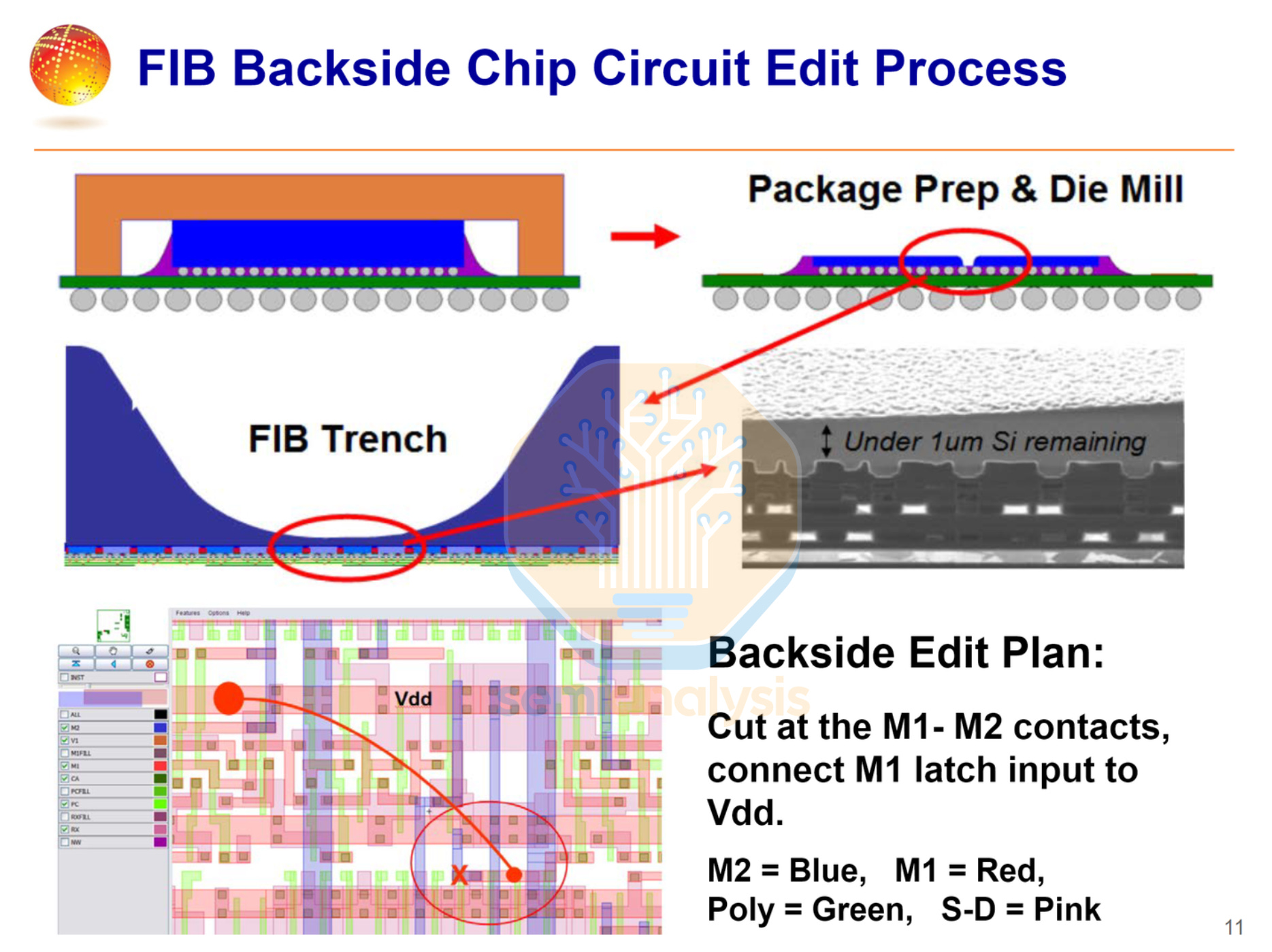
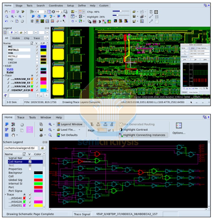
This circuit editing is done with advanced Focused Ion Beam (FIB) tools to add jumper wires or alter transistor interconnect patterns while keeping the chip fully functional so the fix can be tested. Designs can accommodate this process by having buffer or spare cells and metal lines that leave more wiggle room for fixing routing faults. As this process can be time consuming, it is mostly used to physically validate the layout changes that are planned to go into the next stepping.
Binning
The last step is speed binning, where each chip is tested at progressively higher frequencies, and those that pass at the highest clocks are sold as premium parts. This performance spread is the result of natural variability in manufacturing. While all the chips at this stage are fully functional, some may require slightly higher voltage than others to achieve the target operating frequency. Binning also encompasses yield harvesting, where some cores or sub-components in the chip may be defective. These are then fused off and sold at a discount with lower performance.
Binning has allowed Intel to create its product mix, the famous Core i5, i7 and i9 branding for CPUs, while NVIDIA GPUs almost never have all SMs enabled due to yield harvesting.
12. System Integration
Validated chips are then placed in reference boards and connected to devices such as storage and networking, with drivers, BIOS, and OS support qualified with System Level Testing (SLT). The chips are run through various stress testing benchmarks, and typical software applications are run to ensure end-user functionality.
Additionally, these boards are bundled with ES silicon and are sampled with partners and developer to receive early customer feedback. These Reference Validation Platforms (RVP) loop the customer into the development cycle. Major applications developers can start optimizing their software to take advantage of the new chips features and ensure day 1 software support upon the chip’s availability.
13. Production
Once the production ready stepping is qualified with satisfactory yield, the design can finally begin ramping up production and deployed with customers. However, the work does not stop. Failure analysis of defective silicon returned from customers can help iron out the last kinks in the design with minor revisions to the manufacturing flow. Design houses continue to work with TSMC as part of the Continuous Improvement Process (CIP) flows to help improve chip yields. FA engineers use tools such as Synopsys Avalon to map a given defect to the corresponding circuit schematic to identify the affected gates and wires in the design.
EDA in Foundry
Apart from the tools used by the fabless design houses, EDA also features extensively in the Foundry as they simulate and design the next generation of process nodes. On top of that, tight collaboration between foundry and fabless companies in the form of DTCO and STCO are used to squeeze even more PPA from the foundry process.
Technology CAD (TCAD) is the physics simulation layer that lets engineers design new transistor architectures entirely in software before spending tens of millions of dollars on silicon experiments. The dominant tool suite is Synopsys Sentaurus, which has two core engines working in sequence. Sentaurus Process simulates every physical fabrication step. Ion implantation, oxidation, thin-film deposition, plasma etching, lithography patterning and predicts the resulting 3D structure of the device down to nanometer-scale dopant profiles. Feed in a process recipe and it simulates the output device geometry.
Sentaurus Device then takes that 3D structure and simulates its electrical behavior, with I-V curves, capacitance, leakage current and breakdown voltage. Together, they let process engineers iterate on complex transistor designs, crucial in the Gate-All Around generation and beyond to CFET and novel materials such as Ruthenium, featured in our IEDM 2025 coverage.
Synopsys Mystic then takes the simulated transistor and extracts compact model parameters (industry-standard SPICE models like BSIM-CMG) from the output. The device simulations are used to form the earliest PDK 0.1 for circuit designers to get started months before any real silicon exists.
Zooming into the atomic frontier, Synopsys QuantumATK is used in materials research, simulating at the scale of individual atoms. It uses density functional theory (DFT) and non-equilibrium Green’s function (NEGF) methods to model quantum transport and electron tunnelling to for material interface engineering. This is particularly useful in Work Function Metallization schemes that precisely control the transistor threshold voltage.
Design Feedback Loop
Silicon measurement data such as transistor characteristics, IR drop and yield maps of chips made on the current process node feed directly back into the foundry’s next-generation PDK development and the design team’s planning for future node updates. Best Known Methods (BKMs) are refined over the lifetime of the node to help customers improve yields and lower costs for the foundry. This forms a productive feedback loop where customers help define the next generation of foundry processes.
DTCO: Blending Process and Design
For decades, chip manufacturing followed a strict handoff. Process engineers developed the transistor technology, characterized it, then “threw it over the wall” to chip designers. The designers worked with whatever they got. Design Technology Co-Optimization (DTCO) demolishes this wall. It evaluates process options using chip-level PPA metrics from the very first day of process development.
The DTCO flow chains the entire tool stack into a feedback loop: Sentaurus TCAD (device physics) → Mystic (PDK) → SiliconSmart/HSPICE (cell characterization) → IC Compiler II/StarRC/PrimeTime (chip-level PPA evaluation), where the results feed back to the process engineers. Process knobs are tweaked to push design rules beyond the conservative cookie cutter standard cells. The biggest companies such as Apple, NVIDIA and AMD have dedicated foundry departments that work closely with TSMC to engineer their own custom cell libraries to push PPA by as much as 15% over standard libraries. Routability improvements translate directly to lower delay, higher performance, lower power and even reduced area from higher area utilization in congested routing zones.
New transistor schemes such as TSMC’s FinFLEX and NanoFlex make DTCO almost mandatory to effectively utilize alternating rows of transistors with significantly different performance and leakage characteristics. Backside power designs with Intel 18A and TSMC A16 expose another dimension of signal and power routing, potentially unlocking new standard cell routing schemes that route around both sides of the transistor layer.
STCO: Co-Optimizing the Entire System
System Technology Co-Optimization (STCO) extends the DTCO concept up one more level, from chip and process co-design to system and package co-design. It addresses chiplet partitioning decisions, packaging technology selection, cross-chiplet bandwidth and latency tradeoffs, multi-die thermal management and power integrity across the entire package. As single die scaling hits economic and physical limits, STCO is how the industry keeps delivering generational performance gains.
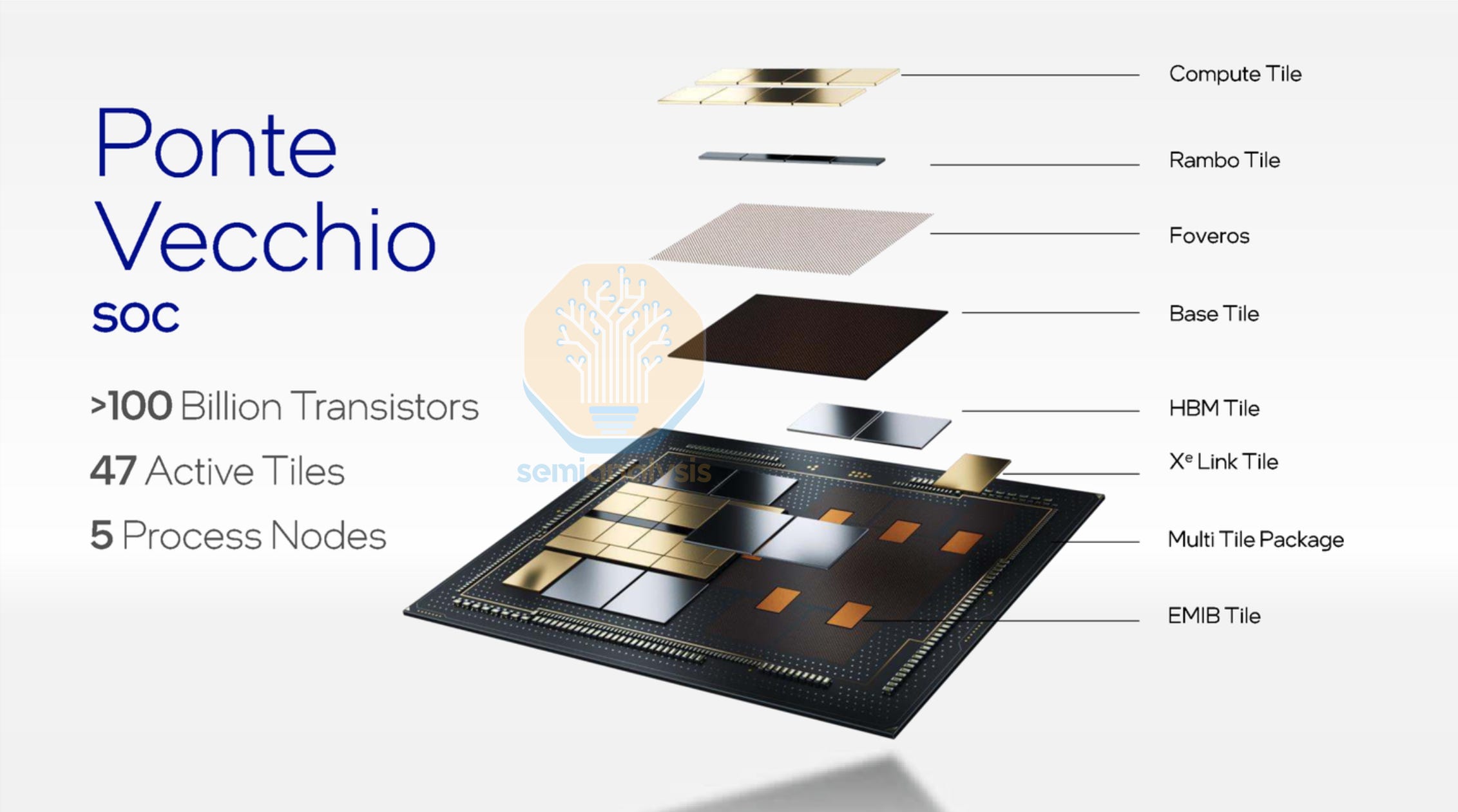
Intel’s Ponte Vecchio GPU is the poster child for a chip that required extensive STCO. It integrates 47 active dies manufactured across five different process nodes, stitched together using both EMIB (Embedded Multi-die Interconnect Bridge, a 2.5D silicon bridge) and Foveros (Intel’s 3D face-to-face die stacking). However, the chip faced several design challenges and was delayed for years, with final performance coming nowhere near original targets. With proper STCO and sound design practices, complex designs can now come out on schedule and on target, which is what AMD plans to do with their MI455X GPU releasing later in 2026.
Below, we discuss the reality of chip design in the real world, and the challenges engineers face from increased design complexity while pushing for compressed design cycles. We also take a look at the hardware that EDA tools run on in simulation and emulation.