

TSMC Overseas Fabs – A Success?
Why Morris Chang Said U.S. Fabs Will Fail, Wafer Cost and Economics of Taiwan vs. U.S. Fabs, TSMC Supply Chain Details
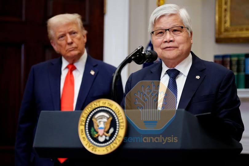
Earlier this year, U.S. President Donald Trump called TSMC “one of the most important businesses in the world.” Although he was incorrect, TSMC is the most important business in the world, his government and others do realize the importance of bringing TSMC into their countries.
This drive to on-shore advanced semiconductor manufacturing has spawned three TSMC overseas ventures: in the United States, Japan, and Germany.
Five years on, these projects are all yielding wafers. But at what cost? Have both TSMC (and by extension, Taiwan) and these foreign countries achieved their goals? Are the overseas fabs economically competitive? Dr. Morris Chang, the company’s legendary founder, has been pessimistic on the U.S. fabs (emphasis added):
…We think that the recent effort of the U.S. to increase onshore manufacturing of semiconductors, right now you’re talking about spending only tens of billions of dollars of money of subsidy. Well, it’s not going to be enough. I think it will be a very expensive exercise in futility
With the fabs operating in high volume, we can finally answer all of that and more in this report. First, some details on what makes TSMC successful, including their history, culture, and structure. Next a discussion of the “clustering” effect that makes Hsinchu Science Park the semiconductor epicenter of the world, and Arizona’s progress towards replicating it, including a detailed look at the supply chains in both places. Finally, we’ll detail the economics of the TSMC Arizona fab - is it truly more expensive to make wafers in the U.S.?
Taiwanese Roots
TSMC operates as a global leader in semiconductor manufacturing, collaborating with hundreds of international clients. Yet, unlike many multinational corporations, it remains deeply Taiwanese at its core, with operations and talent overwhelmingly concentrated on the island.
Of TSMC’s 83,000+ global employees, close to 90% are Taiwanese, including 88% of management-level staff. By location, 87% of employees work in Taiwan. The next-largest groups are based in China, the United States, and Japan.
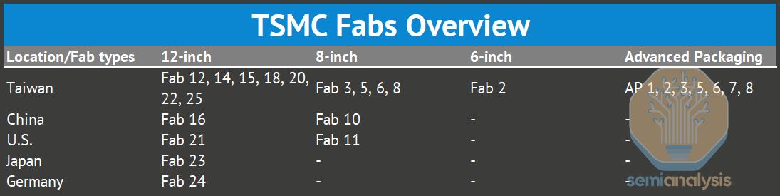
In manufacturing, over 90% of TSMC’s total capacity is in Taiwan—meaning that this small island supports more than 60% of the world’s semiconductor output and over 90% of global advanced-node capacity.
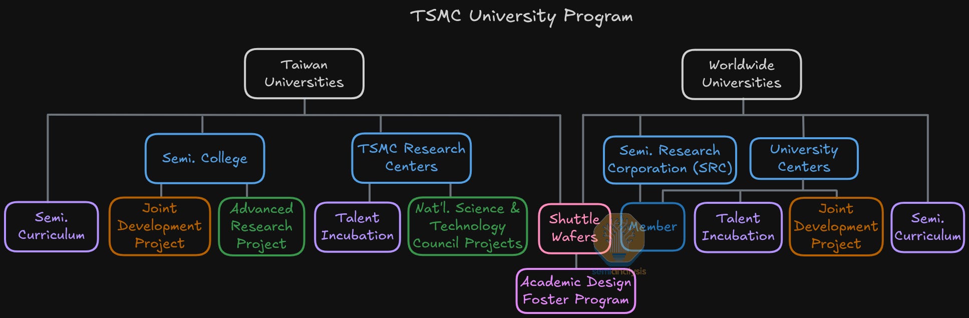
Even as TSMC expands globally, Taiwan remains its largest talent base. It’s not just their base of operations, the company’s talent pipeline is also Taiwanese. With strong government support, TSMC has launched 57 semiconductor programs across 17 local universities, covering areas from fundamental science to advanced packaging. It also provides process design kits (PDKs) for educational use, ensuring a steady pipeline of skilled young engineers for the future.
World-class corporate governance
TSMC has also demonstrated world-class corporate governance throughout its 38-year history. It was clear even from the initial vision for the company:
When I founded a semiconductor company, there was only one path: to make it a world-class one.
-Dr. Morris Chang, TSMC founder
Unlike most Taiwanese companies - where boards are often dominated by major shareholders - Morris emphasized professional governance and independence from the start. When founding TSMC, he designed a board structure grounded in two key principles:
Directors should possess semiconductor industry expertise, and
Independent directors must remain free from both management influence and major shareholders.
Today, TSMC’s 10-member board reflects that philosophy: 7 members are independent directors. Of the total, 4 are Taiwanese—including Chairman C.C. Wei, former CEO F.C. Tseng, and a representative of the Taiwanese government. The remaining members comprise five from the U.S. and one from the U.K.
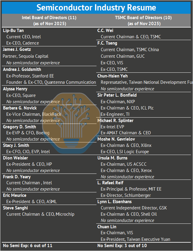
Compare this to the board that presided over Intel’s decade+ of disastrous choices: 7 members, more than half, had no semiconductor experience whatsoever. Including the chairman!
At the operational level, 26 of TSMC’s 30 core executives are Taiwanese, yet most hold advanced degrees from leading U.S. universities in science or engineering. This blend of local leadership and global education reinforces TSMC’s reputation as both an international company and a Taiwanese success story.
WaferTech
TSMC’s Arizona fab isn’t the company’s first U.S. production site. In 1996, TSMC founder Dr. Morris Chang decided to establish WaferTech as a joint-venture fab in Camas, Washington, alongside three clients: Altera, Analog Devices, and ISSI. These clients had urged TSMC to expand its capacity proactively.
From 1990-1999, TSMC achieved a CAGR of nearly 45%, with 1995 revenue at $1.1B and net margin of $500M. These results gave company leaders the confidence to invest in a U.S. fab. According to Dr. Chang’s 2024 biography, they knew costs would be higher than Taiwan but, for reasons unclear, assumed margin would remain acceptable.
Reality soon proved otherwise:
Initially it was chaos, it was just a series of ugly surprises because when we first went in, we really expected the costs to be comparable to Taiwan. And that was extremely naive.
-Morris Chang on early years of the WaferTech venture
After groundbreaking, nearly every cost exceeded estimates, and coordination between the WaferTech management team and TSMC headquarters in Taiwan became strained. TSMC’s Senior Vice President of Operations, Steve, Tso, was tapped to stabilize the project. It took four years to normalize operations, and profit margin on identical products remained 20–25% lower than at TSMC’s Taiwan fabs.
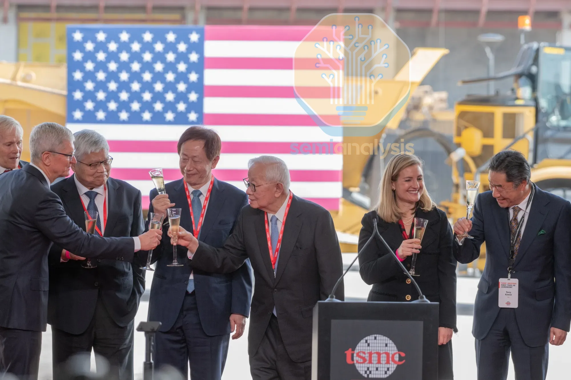
At the December 2022 tool-in ceremony for TSMC Arizona, Morris Chang “reminisced” on the WaferTech project:
[WaferTech] was, I thought, a dream fulfilled. However, we ran into cost problems. We ran into people problems. We ran into cultural problems. And before long, the dream fulfilled became a nightmare fulfilled. [nervous laughter from the crowd]
(In the full unofficial transcription of his speech he also calls globalization and free trade “almost dead” and reveals that even at the start of TSMC, he dreamed of building fabs in America)
But he also said the company was far better prepared this time. Still, the WaferTech precedent led to skepticism, both internal and external, on the Arizona project 20 years later.
Morris Chang & Arizona
Although Dr. Chang officially retired from TSMC in 2018, he still holds influence over major company decisions. With unmatched experience, he is, deservedly, a legend in the industry.
The decision to build the Arizona fab was made in 2020 by his successor, Mark Liu, who went on to retire in 2024. Dr. Chang likely approved, or at least didn’t explicitly block, the project, but was publicly skeptical in the project’s infancy.
On the same podcast where he called the U.S. fabs “an exercise in futility,” Chang further detailed why the built the fab and what he thought of its economics (emphasis added):
We [built the Arizona fab] at the urging of the U.S. government, and we felt that we should do it
The U.S. will increase onshore manufacturing of semiconductors somewhat. But all of that will be very high-cost increase, high unit cost. It will be noncompetitive in the world markets where you compete with factories like TSMC.
We see this statement as an honest reflection of Dr. Chang’s long-standing belief that TSMC’s success depends on its cluster efficiency in Taiwan. This cannot be easily replicated abroad. More discussion on clusters in a few sections…
Concerns with Overseas Expansions
It’s not just Morris Chang who is has doubts. The Arizona project, far larger in scale than WaferTech, has drawn intense scrutiny both inside and outside the company. Most concerns center on TSMC Arizona’s ability to achieve similar operational efficiencies to the Taiwan fabs.
As Dr. Cliff Hou, TSMC’s SVP and Co-COO, explained at SEMICON Taiwan 2025,
The winning model of TSMC is driven by its complete ‘one-hour semiconductor ecosystem’ across Taiwan’s science parks, enabling easy communication with suppliers and partners, and allowing TSMC to obtain anything it needs within an hour.
While Taiwan has an amazing high speed rail system. Americans take 1 hour just to cross a single metro in a car and supply chains are geographically dispersed across thousands of miles, accessible only via air travel. Beyond cost concerns, labor availability and the relative absence of a mature local ecosystem remain major challenges. During the global chip shortage and rising geopolitical tensions with China, the U.S. government pushed TSMC to build local capacity, making this expansion not only a business decision but also a strategic and political one.
In Taiwan, both the government and the public have voiced anxiety that transferring advanced technologies abroad could weaken national sovereignty. While the government takes pride in TSMC’s global leadership and its role as a “silicon shield,” it has also tried to downplay the term to avoid heightening cross-strait tensions.
Taiwan Semiconductor Cluster
The semiconductor foundry business, like most manufacturing industries, is driven by efficiency. Success depends on achieving the highest possible yield and fab utilization. To maximize yield, a foundry needs highly skilled engineers and a tightly integrated supply chain that can troubleshoot and sustain 24/7 operations.
Taiwan’s semiconductor ecosystem is anchored by three major science parks—Hsinchu, Central (Taichung), and Southern (Tainan). Among them, Hsinchu Science Park serves as the heart of the cluster, accounting for around 60% of Taiwan’s semiconductor output value. It is home to TSMC’s headquarters and R&D center and hosts no fewer than 189 semiconductor-related companies, including 95 IC design firms, 17 foundries, and 17 testing and packaging houses.
The Central and Southern clusters further support advanced-node and advanced-packaging production. The maximum distance between any 2 TSMC fabs in Taiwan is less than three hours by car, enabling fast coordination and resource sharing.
Looking at suppliers, most of TSMC’s tier-1 suppliers - those providing raw materials, equipment, and services directly - operate factories in Taiwan. This geographic concentration minimizes logistics delays. TSMC Taiwan has achieved, more completely than any competitor or location, the “one hour” ecosystem.
Arizona Cluster
Although the Trump and Biden administrations have continually pushed to bring the semiconductor ecosystem back to the United States, with many suppliers following TSMC to Arizona, the cluster there still has a long way to go.
According to data from the Semiconductor Industry Association, most of TSMC’s raw material suppliers have not yet established facilities in Arizona. As a result, TSMC continues to rely largely on its supply chain and engineering in Asia. This limits the potential production scale of its Arizona fab until local suppliers scale up significantly and the CHIPS Act does not have enough money to incentivize a truly vertical supply chain.


The supply-chain spin up hasn’t been totally smooth either. Gas facilities for the AZ fab are outsourced to Linde, rather than an the in-house systems used by TSMC Taiwan. A recent outage at Linde’s facility sent impure process gases into the fab, leading to a multi-million dollar scrap event. TSMC has not disclosed the exact details, but Tim Culpan notes in his writeup that Q3 profit at the fab will be $1.4M, down from $140M in the previous quarter.
TSMC Overseas Plans: U.S., Japan, Europe, … and Beyond?
The company line about overseas fabs is that they are always driven by customer demand. This obscures the fact that the “customers” here are foreign governments trying to diversify geopolitical risks. Traditionally, TSMC would only build capacity in response to real wafer demand from its direct customers.
It may not be TSMC’s preferred method of operating, but it makes sense from a government perspective. As we’ve said before, bringing advanced logic capacity on-shore is an economic and national security imperative:
According to the director of the National Economic Council, the 2021 chip shortage cost 1% of U.S. GDP that year – about $240B. That was a months-long disruption, mostly in mature chips. Restoring advanced logic capabilities from zero would take decades. If the 2021 shortage was a 10-foot swell, zeroing out advanced logic supply would be a 100-foot tsunami.
8 of the 10 largest companies in the world depend in large part on TSMC for their business (the 9th is TSMC itself). Together, more than 1/3rd of their combined $2T in revenue comes from hardware that requires TSMC products. That alone is 3% of U.S. GDP dependent on 1 square mile in southern Taiwan. Bear in mind this is only a portion of the companies beholden to TSMC Taiwan production. Furthermore the entirety of the digital economy, automotive economy, and industrial production economy relies on chips from TSMC. The world economy would grind to a halt without TSMC.
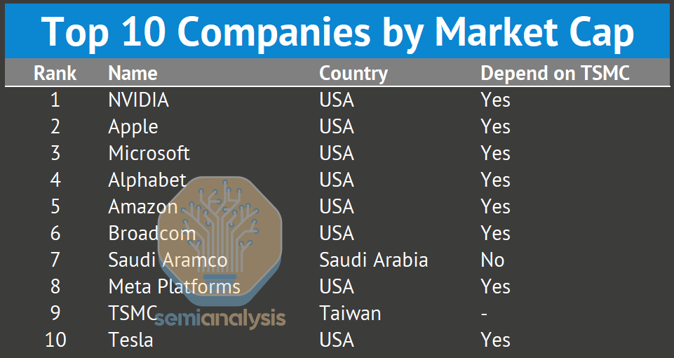
Even Saudi Aramco, the one company not directly dependent on TSMC, can not control their oil wells and refining capacity or do exploration without semiconductors from TSMC.
The U.S. and other governments recognize this and are attempting to reduce exposure, mostly by subsidizing TSMC to build a fab in their country. The Arizona project is by far the largest investment as it focuses on more advanced nodes, but operations and further expansions are underway in Japan (JASM) and Germany (ESMC) as well.
JASM produces the legacy 28 and 16nm nodes, planar and older finFET architectures, for specialty applications like CMOS image sensors and automotive. Sony is the main client. Phase 1 entered high volume production this year, phase 2 is planned and likely introduces 7nm-class, EUV-using nodes (N6).


ESMC is similar to JASM, running 28 and 16nm-class nodes, but with a focus on Bosch and other European customers. Fab shell construction is underway for the first and only planned phase.


As TSMC announced earlier this year that it will expand its U.S. investment to $165B, industry rumors suggest the possibility of adding additional phases in Arizona. Rumors suggest 6 more phases, bringing the total to 12, starting construction in 2032. If completed, this would make TSMC Arizona the largest advanced fab in the world.
To achieve this scale, however, the current supply chain cluster will need significant expansion, cost reductions in raw materials, and improvements in talent recruitment. These challenges will require coordinated efforts from TSMC, its suppliers, and the U.S. government.


Possible UAE Fab
In May 2025, Bloomberg News reported a rumor that TSMC was in discussions with White House officials about the possibility of building an advanced-node fab in the United Arab Emirates (UAE). However, at the June 2025 shareholders’ meeting, CEO C.C. Wei clarified that TSMC had no plans to build a fab in the Middle East.
Talks reportedly collapsed because Washington wanted sovereign control over the proposed site, which the UAE would not accept, along with concerns about IP and technology leaking from a more China-friendly nation.
U.S. involvement stemmed from the CHIPS Guardrails Rule (2023), which prohibits any expansion of non-legacy semiconductor capacity in “foreign countries of concern” without prior U.S. approval. The rule aims to control the transfer of advanced-node technology and prevent it from reaching restricted regions.
Building in the UAE might also have affected TSMC’s Arizona plans due to limited labor availability, there are only so many Taiwanese engineers available to spin up a foreign fab. The Middle East lacks a mature semiconductor supply chain and training or recruiting local engineers would pose major operational challenges. Even if the company eventually built a facility there, it would likely be limited in scale.
Arizona Yield Ramp
The speed of yield ramp-up is a key indicator of a foundry’s operational efficiency - especially for TSMC Arizona as it’s the company’s first advanced-node fab built overseas. In October 2024 Rick Cassidy, CEO of TSMC Arizona, said that the early production yield of chips from the Phoenix facility was about four percentage points higher than that of comparable fabs in Taiwan.
However, several points deserve clarification. The 4 nm production line had already been in volume production in Taiwan for more than two years, meaning that the process parameters were fully optimized before being transferred to Arizona. In addition, the initial product mix was naturally higher yield: AMD compute chiplets and Apple mobile SoCs on the order of 100mm2 were most of the early Arizona production volume, versus Nvidia reticle-size GPUs close to 800mm2 running in Tainan.
Even so, competitive yield on an aggressive ramp timeline is a positive signal for the Arizona project.
Arizona Fab Construction
A core part of TSMC’s operations is building and ramping fabs quickly, repeatably, and at low cost. Their method is mature and well-known to their Taiwan contractors, but had to be ported over for the Arizona project.
TSMC’s fab construction workflow consists of three main phases:
Core and shell building, which includes the foundation, steel superstructure, and external walls but excludes emission units.
Mechanical, electrical, and process piping, covering the installation of operational systems such as the cleanroom and the equipment inside it.
Tool hookup, involving the connection of piping and electrical systems that support semiconductor manufacturing equipment.
Unlike other foundries that use the turnkey EPC (Engineering, Procurement, and Construction) model, TSMC prefers an owner-directed contracting approach. Each engineering project is tendered separately, allowing contractors to work directly with TSMC and reducing procedural and communication costs.
The core and shell contract covers substructure work and CSA (Civil/Structural/Architectural) scope. Substructure work includes earthwork and piling, while the CSA scope varies by building type.
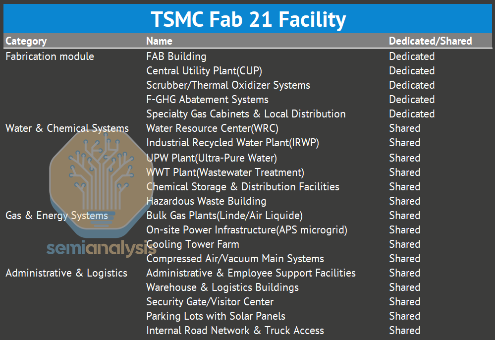
All phases are bid out to construction partners and organized by TSMC’s Facility Division. The Arizona site is planned as a multi-phase development, with each fabrication module containing a dedicated fab building and central utility plant (CUP), while sharing common backbone infrastructure.
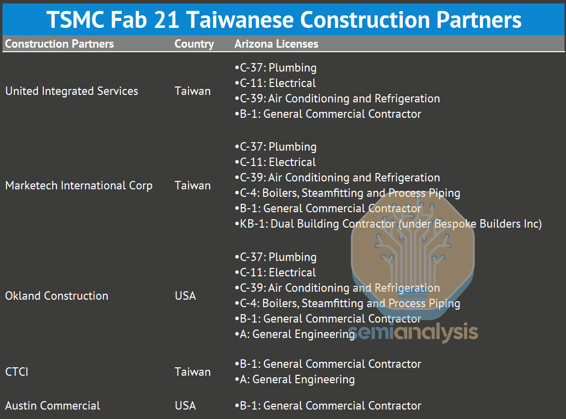
To maintain consistency and schedule, TSMC brought in its long-term construction partners from Taiwan, cultivated over the past decade through major fab projects. Five companies are involved in total—three from Taiwan and two from the United States. Based on their Arizona Registrar of Contractors licenses, we believe United Integrated Services, Marketech International Corp., and Okland Construction are the key contributors.
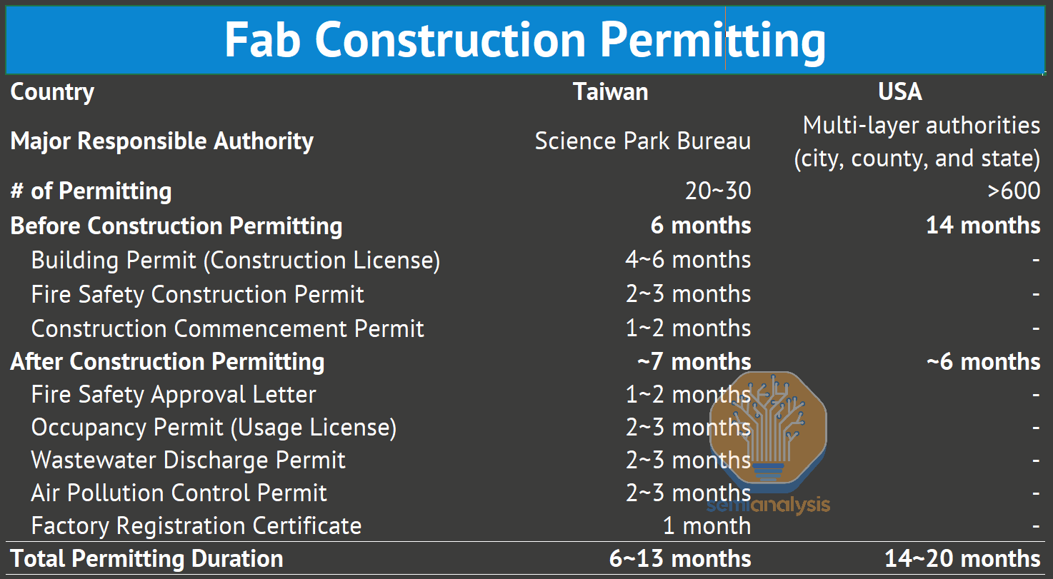
TSMC is currently shortening the interval between Phases 1 and 2, and Phase 3 is expected to finalize its facility engineering contract by the end of 2025. Given pressure from the U.S. government and increased investment commitments to the project, further phases will also be built at a relatively quick cadence. This is not simple as, amongst other challenges, the U.S permitting process takes about twice as long as Taiwan’s.
Notably, Taiwan imposes a maximum time limit on certain permitting requests, ensuring that TSMC can build fabs on a shorter and more predictable timeline.
Next, we’ll discuss the cost of building and operating the TSMC Arizona fab, including specific line items that make it many times more expensive than Taiwanese fabs. We’ll also show how that flows through to cost per wafer and ultimately gross margin of fabs in each locale.