

Intel 18A Details & Cost, Future of DRAM 4F2 vs 3D, Backside Power Adoption (or Not), China's FlipFET, Digital Twins from Atoms to Fabs, and More
VLSI 2025 Roundup
Long time readers will recall that SemiAnalysis covers more than just datacenters and AMD. Today we’re back to semiconductors with a tech-focused roundup of the best from this year’s VLSI conference, the premiere design and integration. That includes the latest in chips manufacturing: fab digital twins, the future of advanced logic transistors and interconnects, DRAM architectures beyond the 1x nm nodes, and more. We’ll discuss Intel’s 18A process and compare with TSMC, where backside power will be adopted (and where it won’t), and the likely winners in 4F2 versus 3D DRAM.
Digital Twins: From Atoms to Fabs
Semiconductor design and fabrication is getting exponentially more complex, increasing development costs and lengthening design cycles. Digital twins allow for design exploration and optimization to be done in an accelerated virtual environment. With this, engineers can ensure that designs work before any silicon is run through the fab.
Digital twins span the entire scale of semiconductor design:
Atomic-level: Simulate the quantum and Newtonian interactions between atoms in materials engineering of transistor contacts and gates
Wafer-level: Optimize tool chambers and process recipes in virtual silicon for yield and performance
Fab-level: Maximize fab productivity with orchestrated maintenance and management across the fleet
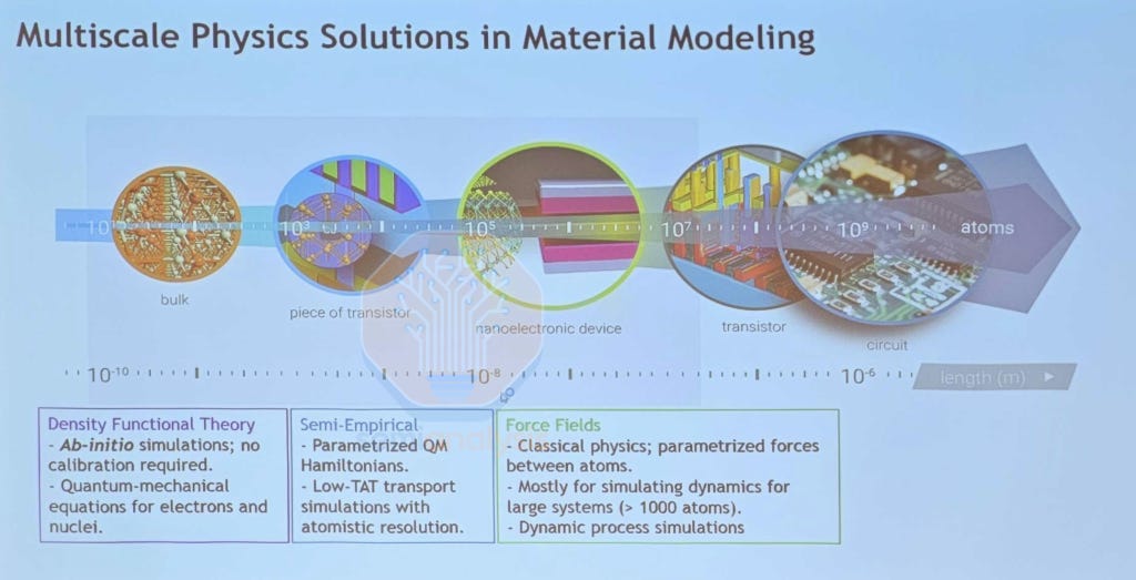
On atomistic simulations, Synopsys provided an overview of their QuantumATK suite, used in materials engineering in transistor contacts and gate oxide stack design, which are critical to device performance. Traditional Density Functional Theory (DFT) modelling of quantum effects between atoms is the most accurate but computationally expensive, while conventional force field simulation of Newtonian atomic interactions is quick but with limited accuracy. GPU accelerated DFT-NEGF (Non-Equilibrium Green’s Function) demonstrated a 9.3x speedup using only 4x A100 vs CPU, while Machine-Learned Force Field simulation using Moment Tensor Potentials demonstrated near-DFT accuracy with 17 min compute cost vs 12 days with traditional DFT.
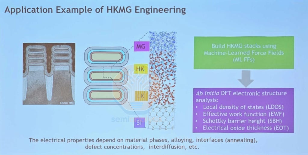
These atomic models are critical in understanding the electrical interactions occurring at the interface between different material layers. In contact engineering, MLFF is used to generate the contact interface between crystalline silicon and amorphous silicides, simulating the depth of interdiffusion where the boundary undergoes silicidation. DFT-NEGF is then used to calculate contact resistance and current-voltage curves across the interface. For gate oxide design, the complex multi-layer work function metal stack is built using MLFF and simulated to check its structure and chemical composition. Dipole dopants can then be introduced and optimized with DFT, which also does electrostatic analysis to calculate key parameters such as effective work function, Schottky barrier height and equivalent oxide thickness. As we move forward into Gate All Around design schemes, these atomic simulations become even more important in choosing the right materials.
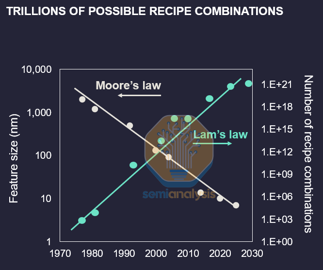
On wafer-level optimization with virtual silicon, Lam Research presented work on their Coventor SEMulator3D software. With transistor geometries increasing in complexity from planar to FinFET to GAA, the number of possible process recipe combinations only grows exponentially, which they’ve marketed as Lam’s Law. Virtual wafer fabrication is done with process simulation using trained models with optimized parameters, allowing engineers to widen process windows and improve yield while reducing the number of physical test wafer cycles required to validate changes. Lam also builds their deposition and etch tools as a digital twin, building virtual chambers with plasma flow simulation to help in recipe prediction while also optimizing chamber design for uniformity across the wafer.
These simulation tools have been used in process window studies to select backside contact schemes with the widest process window while investigating how each recipe affects the stress and strain across the nanosheet transistors. High Aspect Ratio etch schemes also use virtual environments to predict tool output etch profiles for a given input mask pattern. These etch profiles are compared to a target output profile and given a distance which is then minimized with further tests in the digital twin.
Going up to the fab-level, Lam also presented the work needed to achieve a ‘lights-out’ fab. That is a fab that requires no human intervention and as such one can turn the lights off. Tool fleets need to be orchestrated in a virtual twin at near real-time speeds to coordinate tool downtime and maximize fab productivity. The tools themselves need to be ‘self-aware’ with their predictive maintenance, using built-in metrology tools that detect tool alignment and process drift over its lifetime. For a lights-out fab, each tool should target at least 1 year of uninterrupted operation with no human intervention, with automatic recovery after failure and self-requesting maintenance.
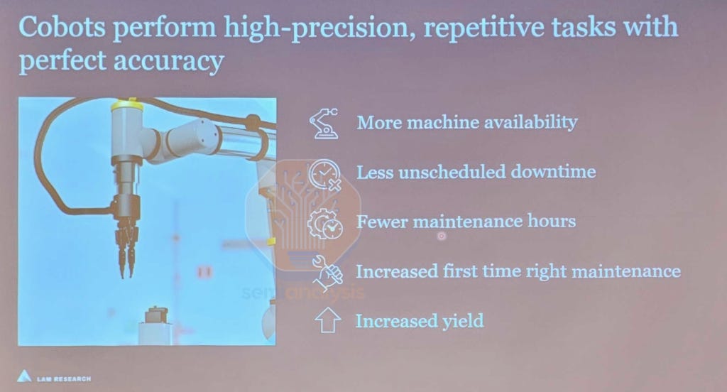
Maintenance of tools would be carried out automatically with robotic parts delivery and installation of consumables and wear items, with tools being designed around robotic maintenance. While a conceptual target of 2035-2040 was given by Lam, the main barrier facing lights-out fabs is with data and connectivity across tools from different vendors and the standardization of maintenance processes.
TSMC DRAM in BEOL
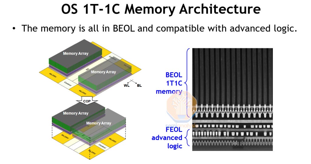
With SRAM bit density no longer increasing with new process nodes, TSMC R&D sought to revive eDRAM to boost chip cache densites. Embedded DRAM was last seen in IBM’s z15 on GlobalFoundries 14nm. The main innovation here is that TSMC can fabricate the entire memory array within the BEOL metal layers, with the DRAM transistor and capacitor formation scheme being within the 400 degree C limit of BEOL flows. This frees up the front-side transistors and lower metal layers for functional logic blocks. With modern processor designs increasing the ratio of SRAM to logic area, being able to stack a DRAM-based last level cache on top of active logic would represent a breakthrough in scalability and design.
However, the demonstration shown is still early in the R&D phase, with the available advanced logic area below just used to house the DRAM peripheral logic (Wordline drivers and sense amplifiers) to boost memory density. The 4Mbit macro that was fabricated only had a bit density of 63.7 Mb/mm2, not even 2x that of modern high density 6T SRAM. For reference, Micron’s latest 1-gamma DRAM would be about 9x denser than this, but without the performance and accessibility to serve as on-die cache.
While TSMC did not give any hints on when this will be ready for productization, it does show huge potential for future generations of this technology, which will fundamentally change how chips are designed.
DRAM: 4F2 and 3D
DRAM has two inflection points on its 5-year roadmap: 4F2 and 3D. The current 6F2, in use for more than a decade, will only scale until the 1d node. With 1c in high volume now, 1d should debut in the next 1-2 years. SK Hynix highlighted a few key challenges in scaling beyond 1d:
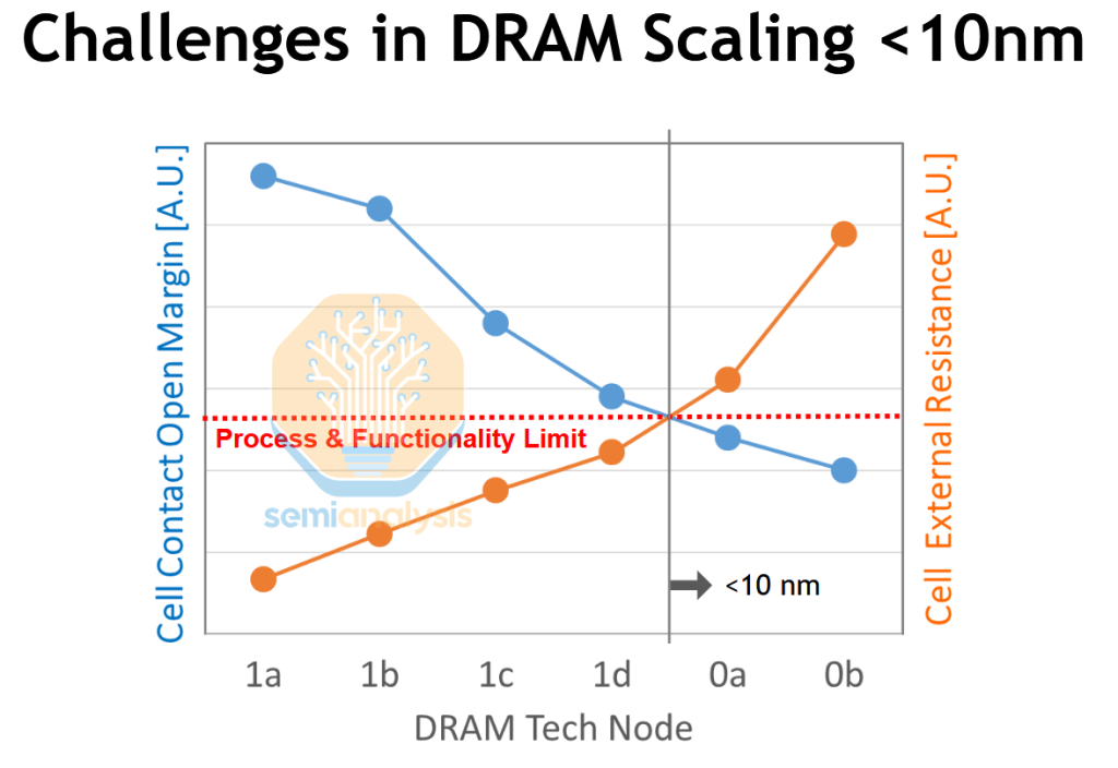
Cell contact areas, in particular the storage node contact where the storage capacitor connects to the control transistor below, shrink quadratically with cell critical dimension. The contacts must be large / well aligned enough to provide a good electrical connection between the transistor and capacitor, but not be so large or misaligned that they short out to any neighboring cells. This is the “cell contact open margin” in the chart above, shrinking with every node. At 1d the process and tooling reach their limits for a workable, high-yield process.
The resistance in the shrinking devices and interconnects also grows as they scale down. This is the “cell external resistance” referenced above. It’s a catch-all sum of all resistive elements between the memory cell and the sense amplifier. The bitline contact and local bitline (metal) wire itself are two main contributors. Both increase in resistance as they scale. This slows down cell operation and reduces the read margin of the cell, both undesirable. Operation speed is affected by charge transfer between the cell and bitline, which slows as the resistance of that path increases. Resistance also saps the voltage differential that the sense amplifier sees. Too little and the cell cannot reliably be read – the memory doesn’t work.

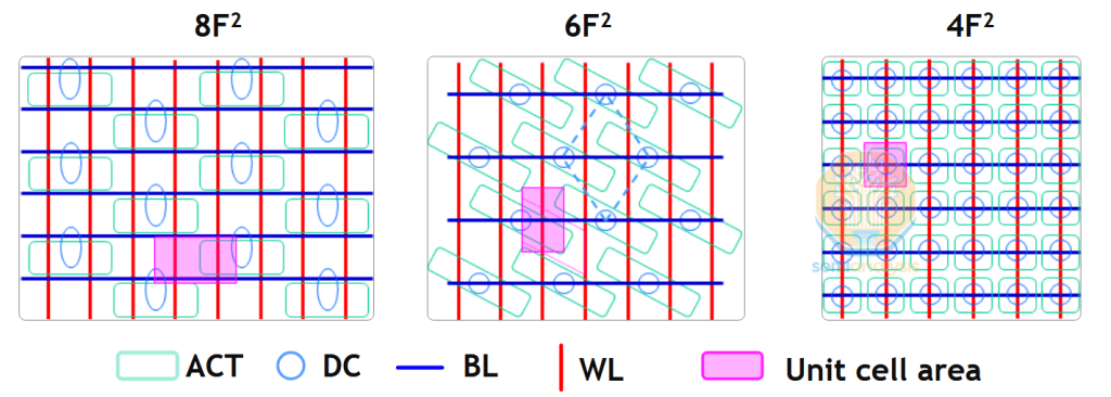
4F2 solves these issues and more. We won’t rehash the basics of the architecture – see our Memory Wall report linked above – but a few specifics are interesting:
The cell contact challenge in 6F2 comes from congestion where the bitline and storage node contact are on the same level (storage node contacts are denoted as BC for buried contact in the image below).
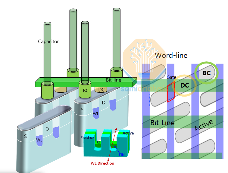
From a side-on view, its easy to see how little margin there is between the bitline and contact:
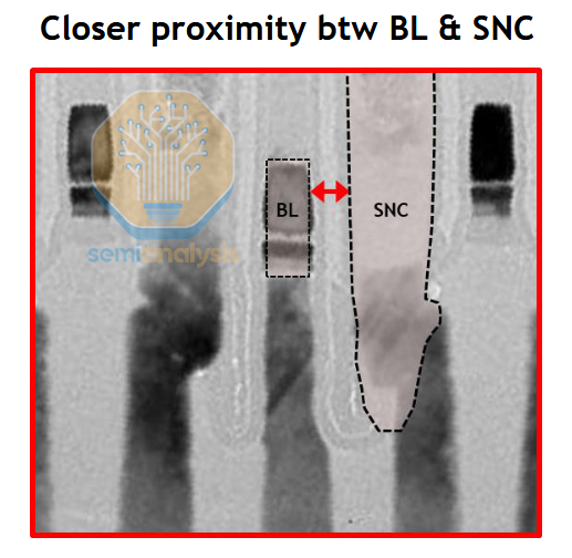
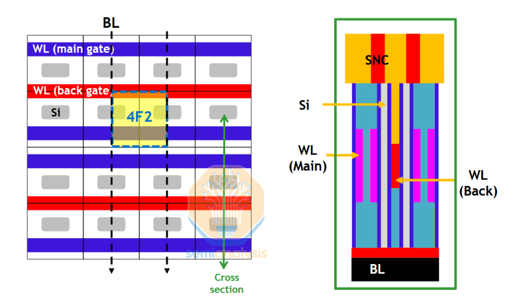
Compare this to vertical channel transistors (VCT) in a 4F2 layout; the buried bitline has its own real estate well out of the way of any other components. The current path is also much shorter, directly down from capacitor, through the vertical channel, directly to the bitline. In 6F2 the path is down through the bottom of the “U” shaped channel and back up, longer and consequently with higher resistance.
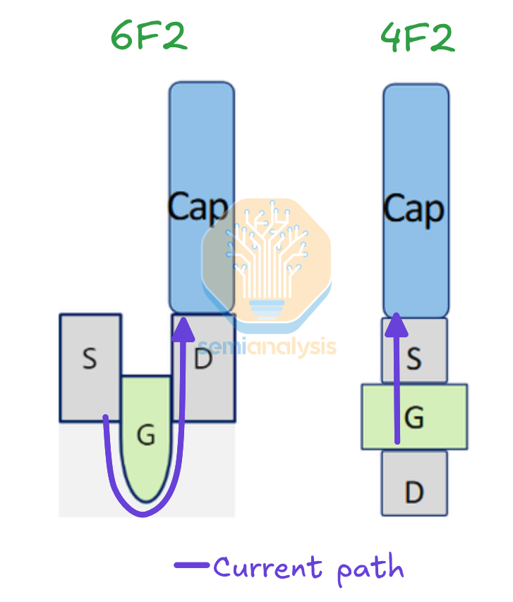
Of course, there are challenges for implementing 4F2 or it would’ve been adopted already. Both the buried bitline and vertical channel transistor are high aspect ratio, difficult for etch and deposition tools. Until just a few years ago deposition tools were not capable of filling a deep trench with the required metals for the bitline, likely Ru or Co. The cell layout, although it reduces some of the alignment challenges, is still denser and thus requires EUV patterning. Last, there was simply no reason to take the risk of changing architectures when 6F2 was still scalable.
There are still a few wildcards in 4F2 development that may determine which fab can achieve lowest cost per bit and good yields, and which tool vendors might benefit. The gate structure, crucial to the performance of the memory cell, might be dual or even gate all around. SK Hynix and others are still deciding.
There is also a choice between peripheral-under-cell and peripheral-on-cell. Conventionally the peripheral circuitry would’ve been adjacent to the memory cells on the wafer frontside, but for increased overall density it will be moved underneath the cell array. Peri-under-cell is similar to backside power for logic, requiring fusion bonding of a second wafer. The control transistors are built in an array on the frontside before a support wafer is bonded on, the wafer flipped, and the peri built up. Then everything is flipped once more to add the storage node contacts and capacitors themselves. The tool vendors who would see incremental benefit are similar to the BSPDN supply chain – CMP, fusion bonding, TSV etch.
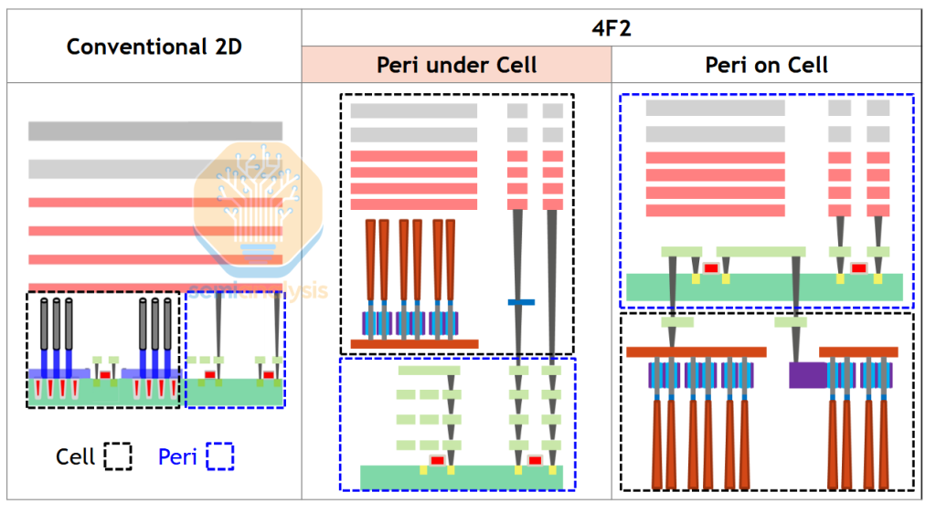
Peri-on-cell is simply hybrid bonding of completed storage node array and peripheral wafers. While this offers some process latitude – the peri can be made without worrying about damage to the array and vice versa – it requires hybrid bonding at a pitch of well below 50nm. That’s an order of magnitude lower than the current leading edge. Still, Hynix at least is looking at it in R&D, and other applications will drive hybrid bonder development regardless.
Last, 3D DRAM is being developed in parallel. Current progress suggests a few nodes of 4F2 are likely before 3D is ready. Chinese chipmakers are a potential disruptor here, as they have strong incentive to develop 3D because it is not dependent on advanced litho.
NVDRAM
Micron’s NVDRAM (NV for non-volatile) resurfaced 18 months after its first appearance at IEDM 2023. This is their ferroelectric (HZO) DRAM using a 4F2 architecture, Ruthenium wordlines, and CMOS under array. If you were trying to make an expensive memory using all the latest tricks, this is probably how you’d do it.
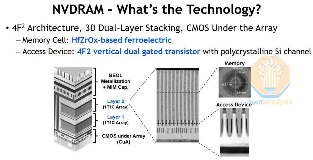
The bitcells were scaled by an impressive 27% since the previous paper, to 41nm on a side, without a degradation in performance. That brings density to nearly 0.6 Gb/mm2, well above any high volume commercial DRAM available today.
Theoretically NVDRAM has a small advantage over traditional DRAM since it does not waste power and time performing refresh cycles. Unfortunately, the electricity savings amount to roughly $1 per year. When a single DIMM is on the order of $300+, the lifetime energy savings are nowhere near enough to justify the higher price of this exotic product. At the very least, the work on Ru wordlines, 4F2, vertical channel transistors, and CMOS under array are all applicable to upcoming DRAM nodes.
2D Materials
Replacing silicon is a high bar. Any replacement must not only yield better performing, denser transistors, it must also be practical to use. Silicon wafers are a commodity and can easily be doped in select areas to form transistor channels. 2D materials are not yet practical to work with on an industrial scale. We’ve written many different times that on-wafer growth is they key blocker. But if chipmakers or labs are solving this problem, they’re keeping it quiet. The papers we saw on other innovations – Intel improving contact formation, Samsung building CFETs with 2D channels – are impressive, but ultimately fall flat if the material can’t be grown in an economic way in the first place.
Forksheet
Gate-all-around is no longer the “next big thing” in logic, it’s ramping towards high volume. Forksheet and CFET have taken the mantle of exciting next-gen architectures. An evolution of GAA, forksheet entails putting the N- and P- halves of a CMOS closer together by adding a dielectric wall between them.
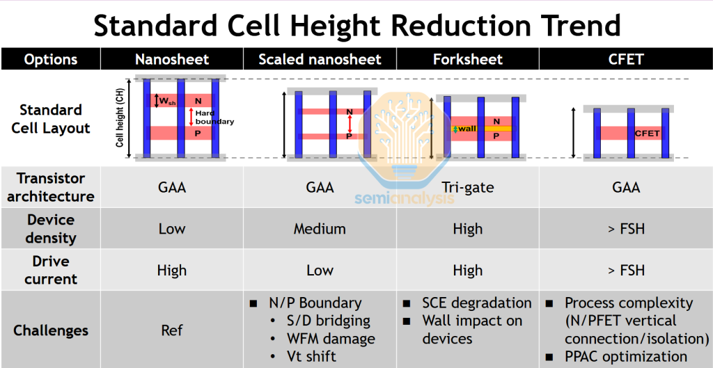
In a traditional architecture, the spacing between NMOS and PMOS devices is limited by parasitic capacitance and the threat of latch-up. Increasing parasitic capacitance means the chip runs slower and uses more power. Latch-up is an outright failure of the transistors giving the input voltage Vdd an uncontrolled path directly to ground. Some techniques already exist – most importantly shallow trench isolation – for mitigating these effects.
Forksheet is a new, theoretically better technique along these same lines. While the material between NMOS and PMOS has always been some sort of insulating dielectric, a forksheet requires an exquisite layer of ultra low-k material to enable tighter spacing. This introduces new integration challenges and extra cost into the manufacturing process.
It’s not trivial to develop a material that can be deposited in nm-thick, high-quality films but also withstand subsequent processing as the rest of the transistor is formed. Plasma-induced damage from etch or deposition is a particular problem. Most papers aren’t detailing their material solutions here but it’s a good bet that AMAT, traditionally the leader in ultra-low-k dielectrics, is playing a part.
Forksheet also nominally has worse gate control than gate-all-around. This is because the gate only wraps around three sides of the transistor channel, the fourth abuts the forksheet wall. It’s basically a finFET turned sideways. Increased density but worse electrostatic control vs. GAA isn’t necessarily a good tradeoff. There are a few workarounds: 1) slightly etch back the forksheet wall, leaving room for gate material to envelop the fourth side of the channel, sacrificing some scaling benefit 2) add additional nanosheets to improve electrostatics control, adding cost and integration complexity.
TSMC, IBM, and IMEC all talked extensively about forksheets. For IBM and IMEC this has limited commercial relevance. For TSMC, a willingness to discuss in detail might even be a negative signal for real adoption. No publicly announced node – through the 14 angstrom families at present – is using forksheet.
CFET Timeline
Even so, the potential successor to forksheet is already being discussed. CFET has been in vogue for a few years and we’ve covered the basics before:
Current work is towards industrialization. Lab demonstrations of a single device work well and look great on slides, but the cost is high and yield low. Even though they are popular at conferences, we think real adoption of CFETs in high volume is still a decade out. A presenter from Intel, in a talk about “beyond RibbonFET,” outright said “We will probably see gate all around for another decade.” As with copper interconnects and finFETs, the core technologies of logic tend to extend 1-2 nodes beyond what is expected.
China’s FlipFET Design
Despite various sanctions, China is not slowing down in semiconductor research and development. Out of all the academic papers presented, Peking University’s FlipFET design caught the most attention, showcasing a novel patterning scheme to achieve similar PPA to CFETs without the headaches of monolithic or sequential integration.
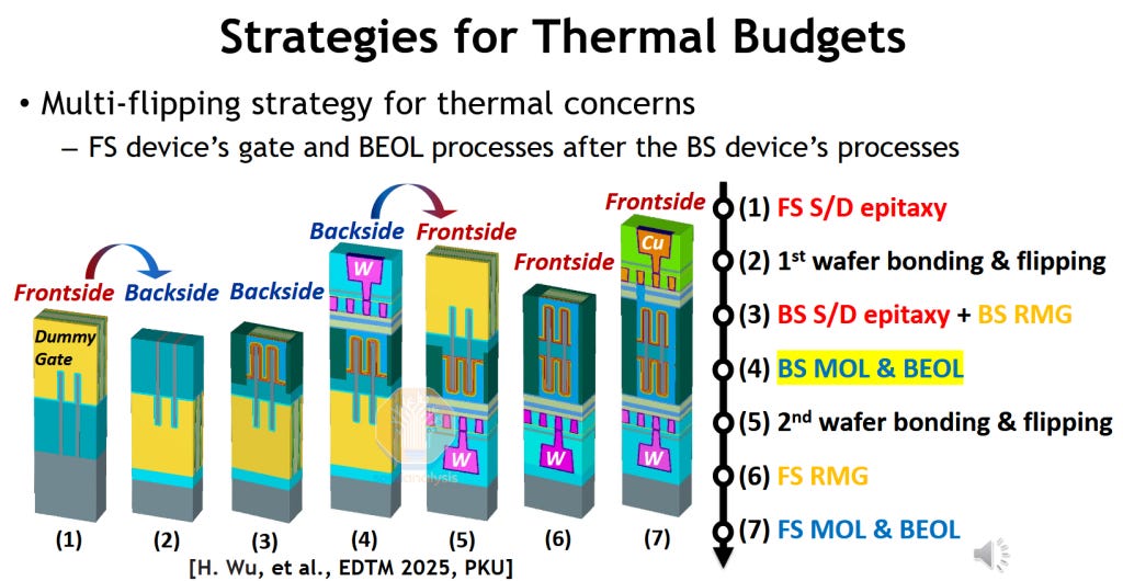
Essentially, the FlipFET concept starts with forming the fins or nanosheets for both top and bottom transistors, but only does the high temperature Source/Drain epitaxy for the top transistor before flipping the wafer and exposing the backside for processing. The contacts and BEOL metal layers are patterned before the wafer is flipped again to complete the lower temperature processes on both sides. This method produces a self-aligned transistor stack that does not need high-aspect ratio processing that monolithic CFETs have to overcome. Forming the gates from both sides also allows easier threshold voltage tuning differences between the top and bottom device.
However, the main drawback to FlipFET is cost, trading off easier integration of the active transistors at the expense of multiple backside process flows with a greater susceptibility to wafer warpage and overlay errors, lowering yield. So far, the lab has only fabricated frontside and backside transistors on separate wafers, leaving doubts on whether the fabrication of the other transistor would affect device performance of the first. Alignment of fine-pitch contacts and metals after wafer flipping is also a concern, but should not be any more challenging than other CFET options.
While the Chinese labs have already demonstrated FlipFETs in silicon, they’re not stopping there. Further innovation of FlipFET designs were presented and modelled such as FlipFET with self-aligned gate, FlipFETs using forksheets with an embedded power rail within the isolation wall, and even applying the FlipFET concept to monolithic CFETs with high aspect ratio Vias to achieve a 4-stack transistor design.
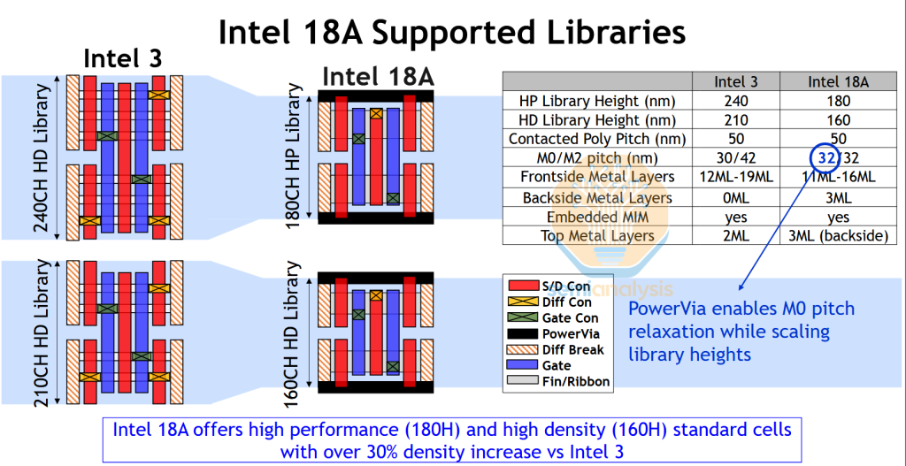
18A Process Details
The star paper was Intel’s 18A presentation. This is the first detailed public look at a real high volume backside power process.
Intel claims 30% SRAM scaling for 18A against an Intel 3 baseline. A large one-time benefit like this is expected when changing from finFET to GAA. The cell diagrams clearly show the shrink achieved by replacing 2 fins with a single stack of wide ribbons:
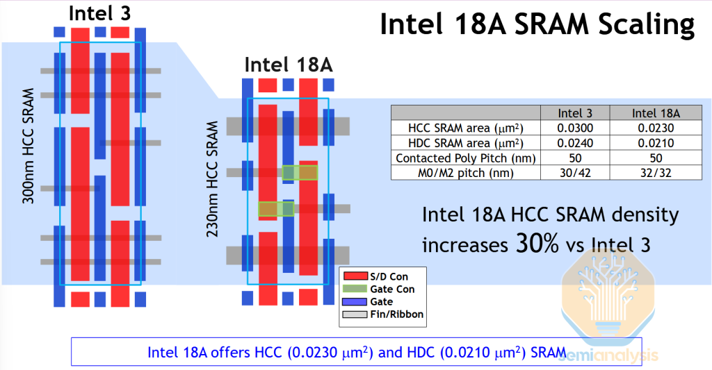
Comparing high density (HD) cell areas, 18A is on par with TSMC N5 and N3E at 0.0210 µm2. N2 should also see at least some benefit from the finFET -> GAA transition, but most of the claimed 22% SRAM scaling (vs. N3E) likely comes from the periphery not the bitcells themselves. Overall 18A density is likely to be slightly less than N3P, and close to 30% less than N2.
18A Cost vs. Leading Nodes
 | A guest post by
|