

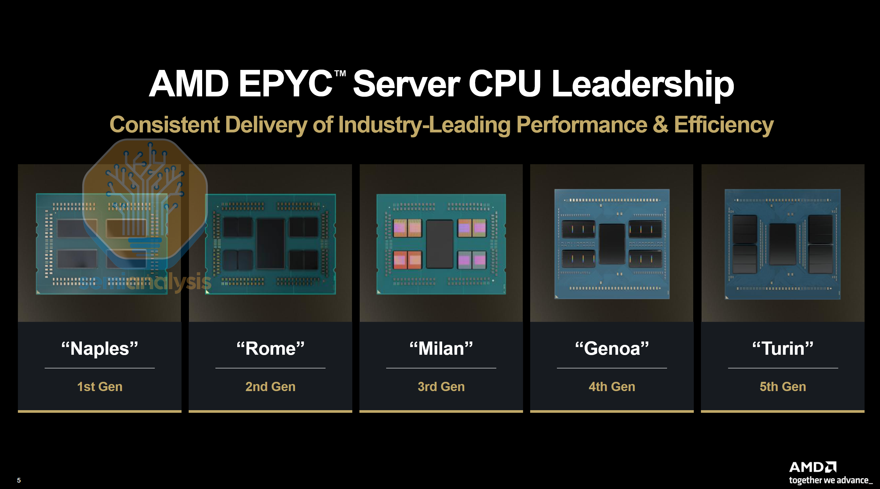
CPUs are Back: The Datacenter CPU Landscape in 2026
RL and Agent Usage, Context Memory Storage, DRAM Pricing Impacts, CPU Interconnect Evolution, AMD Venice, Verano, Florence, Intel Diamond Rapids, Coral Rapids, Arm Phoenix + Venom, Graviton 5, Axion
Since 2023, the datacenter story has been simple. GPUs and networking are king. The arrival and subsequent explosion of AI Training and Inference have shifted compute demands away from the CPU. This meant that Intel, the primary supplier of server CPUs, failed to ride the wave of datacenter buildout and spending. Server CPU revenue remained relatively stagnant as hyperscalers and neoclouds focused on GPUs and datacenter infrastructure.
At the same time, the same hyperscalers have been rolling their own ARM-based datacenter CPUs for their cloud computing services, closing off a significant addressable market for Intel. And within their own x86 turf, Intel’s lackluster execution and uncompetitive performance to rival AMD has further eroded market share. Without a competent AI accelerator offering, Intel was left to tread water while the rest of the industry feasted.
Over the last 6 months this has changed massively. We have posted multiple reports to Core Research and the Tokenomics Model about soaring CPU demand. The primary drivers we have shown and modeled are reinforcement learning and vibe coding’s incredible demand on CPUs. We have also covered major CPU cloud deals by multiple vendors with AI labs. We also have modeling of how many CPUs of what types are being deployed.
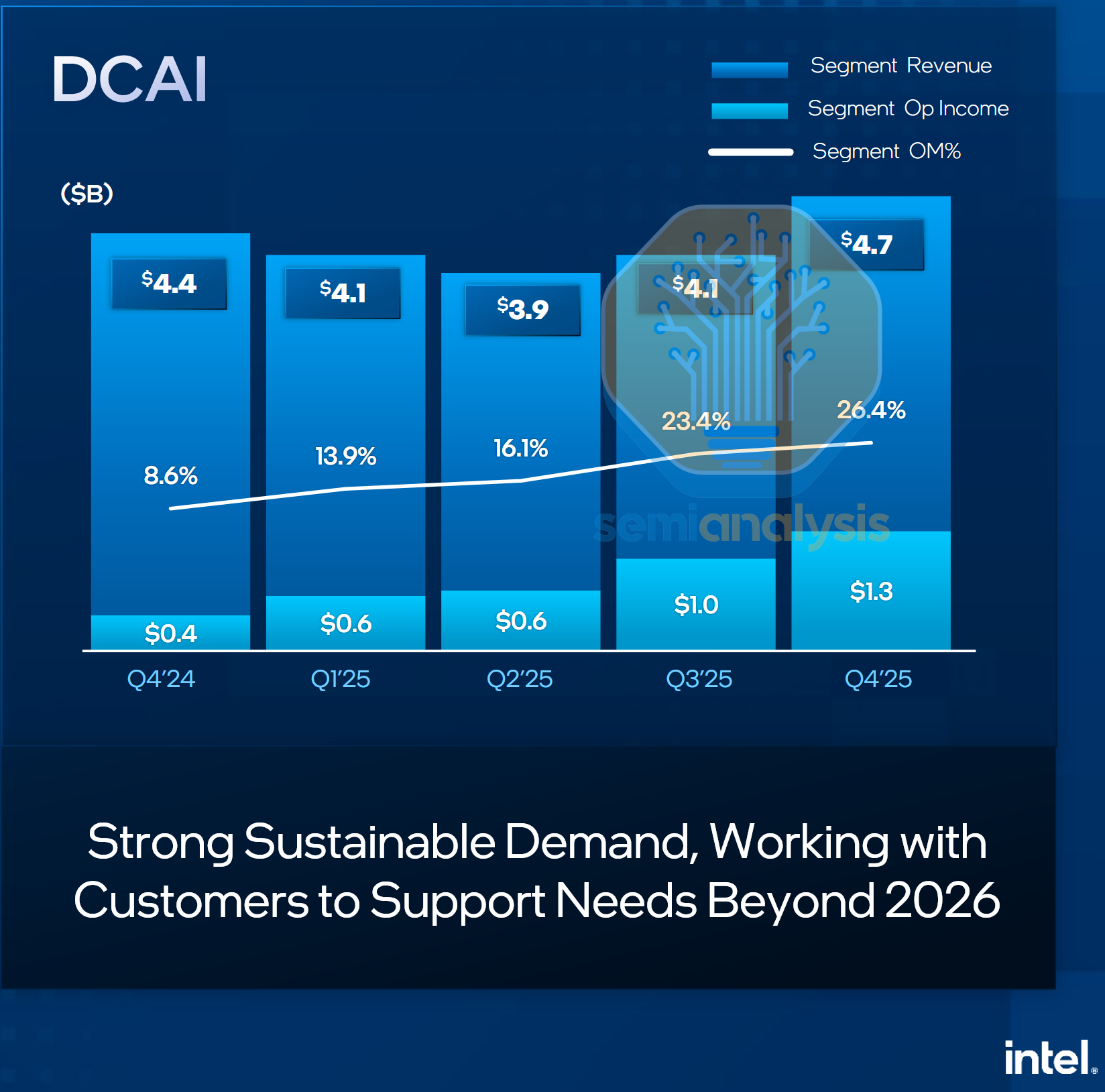
However, Intel’s recent rallies and changing demand signals in the latter part of 2025 have shown that CPUs are now relevant again. In their latest Q4 earnings, Intel saw an unexpected uptick in datacenter CPU demand in late 2025 and are increasing 2026 capex guidance on foundry tools and prioritizing wafers to server from PC to alleviate supply constraints in serving this new demand. This marks an inflection point in the role of CPUs in the datacenter, with AI model training and inference using CPUs more intensively.
2026 is an exciting year for the datacenter CPU, with many new generations launching this year from all vendors amid the boom in demand. As such, this piece serves to paint the CPU landscape in 2026. We lay the groundwork, covering the history of the datacenter CPU and the evolving demand drivers, with deep dives on datacenter CPU architecture changes from Intel and AMD over the years.
We then focus on the 2026 CPUs, with comprehensive breakdowns on Intel’s Clearwater Forest, Diamond Rapids and AMD’s Venice and their interesting convergence (and divergence) in design, discussing the performance differences and previewing our CPU costing analysis.
Next, we detail the ARM competition, including NVIDIA’s Grace and Vera, Amazon’s Graviton line, Microsoft’s Cobalt, Google’s Axion CPU lines, Ampere Computing’s merchant ARM silicon bid and their acquisition by Softbank, ARM’s own Phoenix CPU design and look at Huawei’s home grown Kunpeng CPU efforts.
For our subscribers, we provide our datacenter CPU roadmap to 2028 and detail the datacenter CPUs beyond 2026 from AMD, Intel, ARM and Qualcomm. We then look ahead to what the future looks like for datacenter CPUs, discuss the effects of the DRAM shortage, what NVIDIA’s Bluefield-4 Context Memory Storage platform means for the future of general purpose CPUs, and the key trends to look out for in the CPU market and CPU designs going forward.
The Role and Evolution of Datacenter CPUs
The PC Era
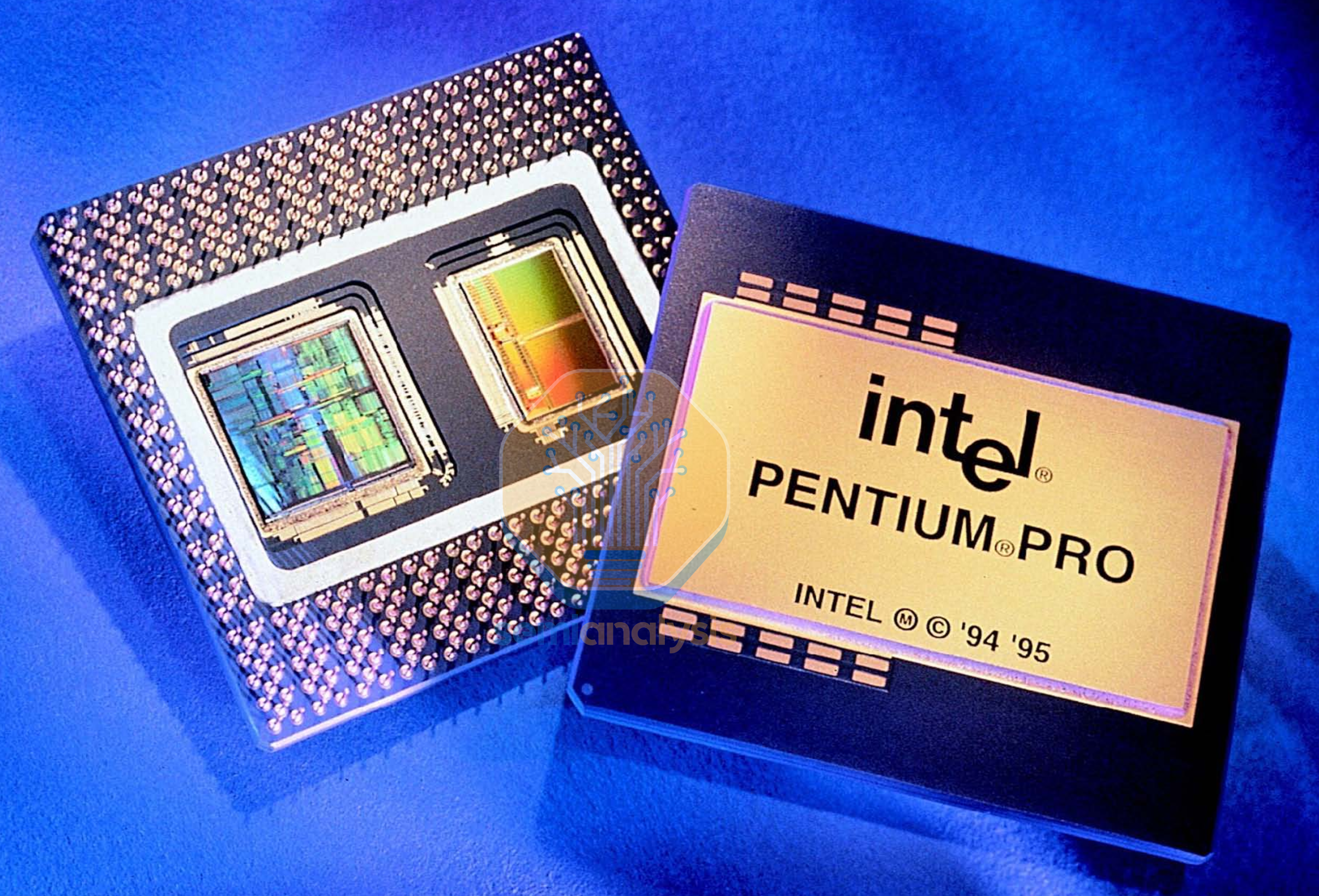
The modern version of the datacenter CPU can be traced back to the 1990s following the success of Personal Computers in the prior decade, bringing basic computing into the home. As PC processing power grew with Intel’s i386, i486 and Pentium generations, many tasks normally computed by advanced workstation and mainframe computers from the likes of DEC and IBM were instead done on PCs at a fraction of the cost. Responding to this need for higher performance “mainframe replacements”, Intel began to release PC processor variants that had more performance and larger caches for higher prices, starting with the Pentium Pro in 1995 that had multiple L2 cache dies co-packaged with the CPU in a Multi-Chip Module (MCM). The Xeon brand then followed suit in 1998, with the Pentium II Xeons that similarly had multiple L2 cache dies added to the CPU processor slot. While mainframes still continue today in the IBM Z lines used for bank transaction verifications and such, they remain a niche corner of the market that we will not cover in this piece.
The Dot Com Era
The 2000s brought the internet age, with the emergence of Web 2.0, e-mail, e-commerce, Google search, smartphones with 3G broadband data, and the need for datacenter CPUs to serve the world’s internet traffic as everything went online. Datacenter CPUs grew into a multi-billion dollar segment. On the design front, after the GHz wars were over with the end of Dennard scaling, attention shifted to multi-core CPUs and increased integration. AMD integrated the memory controller into the CPU silicon, and high-speed IO (PCIe) came directly from the CPU as well. Multi-core CPUs were especially suited for datacenter workloads, where many tasks could be run in parallel across different cores.
We will detail the evolution of how these multiple cores are connected in the interconnect section below. Simultaneous Multi-Threading (SMT) was also introduced in this time by both AMD and Intel, partitioning a core into two logical threads that could operate independently while sharing most core resources, further improving performance in parallelizable datacenter workloads. Those looking for more performance would turn to Multi-socket CPU servers, with Intel’s Quick Path Interconnect (QPI) and AMD’s HyperTransport Direct Connect Architecture in their Opteron CPUs providing coherent links between up to eight sockets per server.
The Virtualization and Cloud Computing Hyperscaler Era
The next major inflection point came with cloud computing in the late 2000s, and was the primary growth driver for datacenter CPU sales throughout the 2010s. Much like how GPU Neoclouds are operating today, computing resources began consolidating toward public cloud providers and hyperscalers such as Amazon’s Web Services (AWS) as customers traded CapEx for OpEx. Spurred by the effects of the Great Recession, many enterprises could not afford to buy and run their own servers to run their software and services.
Cloud computing offered a far more palatable “pay as you use” business model with renting compute instances and running your workloads on 3rd-party hardware, which allowed spending to dynamically adjust with usage that varied over time. This scalability was more favorable than procuring one’s own servers, which needed to be utilized fully at all times to maximize ROI. The Cloud also enabled more streamlined services to emerge, such as serverless computing from the likes of AWS Lambda that automatically allocates software to computing resources, sparing the customer from having to decide on the appropriate number of instances to spin up before running a particular task. With nearly everything handled by them behind the scenes, Clouds turned compute into a commodity.

The key feature for a secure and resource efficient Cloud to work at all is CPU hardware virtualization. In essence, virtualization allows a single CPU to run multiple independent and secure instances of Virtual Machines (VMs) orchestrated through hypervisors such as VMware ESXi. Multi-core CPUs could be partitioned such that each VM would be assigned to a single core or logical thread, with the hypervisor able to migrate instances onto different cores, sockets or servers over the network to optimize for CPU utilization while keeping data and instructions secured from other instances operating on the same CPU.
The need for virtualization for the cloud, combined with CPU designers implementing SMT to boost performance was eventually exploited with the Spectre and Meltdown vulnerabilities in 2018. When two instances ran on threads running on the same physical core, it was possible for an attacker to snoop and piece together data from the other thread using the CPU cores branch prediction functions, a performance boosting technique that guessed, fetched and executed instructions ahead of the running program to keep the CPU busy. With security in the cloud potentially compromised, providers rushed to disable SMT to stop the attack vector. Despite patches and hardware fixes, the performance loss of up to 30% without SMT would haunt Intel and show up in untimely design decisions down the road which we detail below.
The AI GPU and CPU Consolidation Era
Following the COVID boom that boosted internet traffic with way more Zoom calls, e-commerce and more time spent online, datacenter CPU growth was at an all-time high. In the five years leading up to ChatGPT’s launch in November 2022, Intel shipped over 100 Million Xeon Scalable CPUs to cloud and enterprise datacenters.
From then on, AI model training and inference serving would upend the CPU’s role in the datacenter, causing widespread changes in CPU deployment and design strategies. Computing AI models requires lots of matrix multiplication, an operation that can be easily parallelized and done at massive scales on GPUs which had large arrays of vector units originally used to render 3D graphics for games and visualizations.
While accelerator nodes still used host CPUs, the highly structured and relatively simple compute requirements did not take advantage of the CPU’s ability to run branchy, latency sensitive code. And with tens of vector units compared with thousands on GPUs, performance and efficiency was 100-1000x worse on CPU, especially when AI-specific GPUs added MatMul focused Tensor Cores to the mix. Despite Intel’s efforts to add more vector and matrix support with doubled AVX512 ports and dedicated AMX accelerator engines, the CPU was relegated to a support role in the datacenter. However, the internet still had to be served while power in the datacenter got prioritized to GPU compute. As a result, CPUs evolved with the times and were split into two categories.
Head Nodes
The head node CPU’s role is to manage the attached GPUs and keep them fed with data. High per-core performance with large caches and high bandwidth memory and IO are desired to keep tail latencies as low as possible. Dedicated designs such as NVIIDA’s Grace were made with coherent memory access for GPUs to utilize CPU memory as model context Key Value Cache expansions, requiring extremely high CPU to GPU bandwidth. For head nodes, 1 CPU is usually paired with 2 or 4 GPUs in each compute node. Examples include:
1 Vera CPU to 2 Rubin GPUs per superchip
1 Venice CPU to 4 MI455X GPUs per compute tray
1 Graviton5 CPU to 4 Trainium3 per compute tray
2 x86 CPUs to 8 TPUv7 per node
Cloud-Native Socket Consolidation
As GPUs hogged more datacenter power budgets, the need to serve the rest of the internet as efficiently as possible accelerated the development of “Cloud-Native” CPUs. The goal is maximum throughput and requests served per socket at the best efficiency (throughput per Watt). Instead of adding more, newer CPUs to boost total throughput, old, less efficient servers are decommissioned and replaced with a far smaller number of cloud-native CPUs that met the total throughput requirement while sipping a fraction of the power, lowering operating costs and freeing up power budget for more GPU compute.
Socket consolidation ratios of 10:1 or greater can be achieved. Millions of Intel Cascade Lake servers bought during the COVID cloud spend are being retired for the latest AMD and Intel CPUs that process at the same performance level but at less than a fifth of the power.
Design wise, these Cloud-native CPUs target higher core counts with area and power efficient medium-sized cores, and have less cache and IO capabilities compared to traditional CPUs. Intel brought their Atom cores to the datacenter with Sierra Forest. AMD’s Bergamo used a more area and power efficient layout of their Zen4 core. Power efficient ARM-based designs such as AWS Graviton saw great success, while Ampere Computing targeted cloud-native compute with the Altra and AmpereOne lines.
The RL and Agentic Era
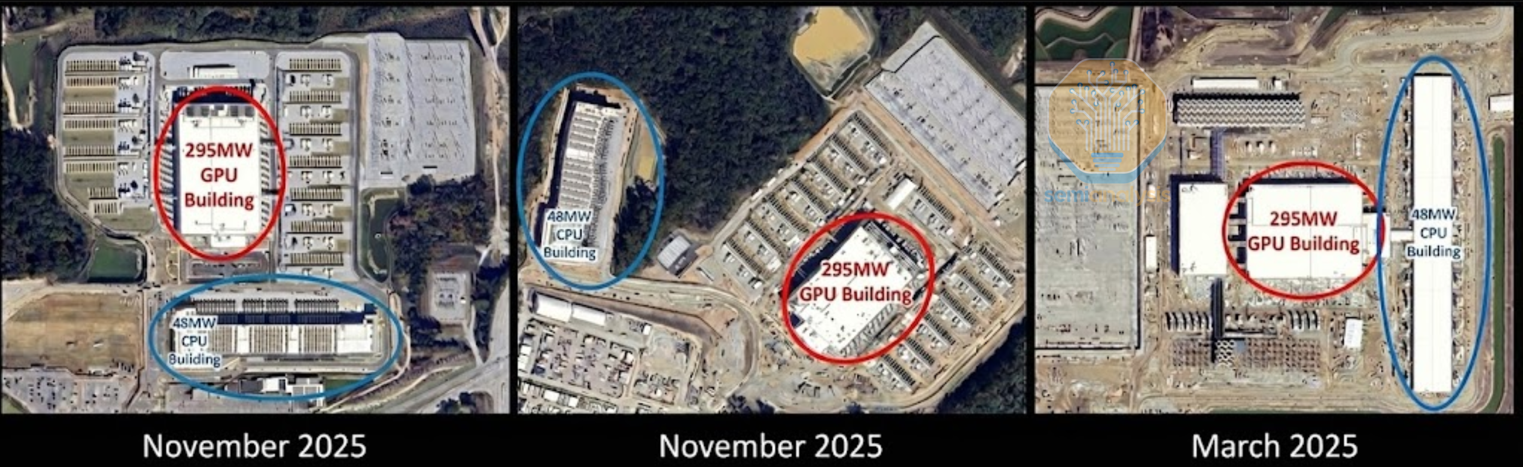
Now, CPU usage is accelerating again to support AI training and inference beyond head nodes. We can already see evidence of this in Microsoft’s “Fairwater” datacenters for OpenAI. Here, a 48MW CPU and storage building supports the main 295MW GPU cluster. This means tens of thousands of CPUs are now needed to process and manage the Petabytes of data generated by the GPUs, a use case that wouldn’t have otherwise been required without AI.
The evolution of AI computing paradigms has caused this increase in CPU usage intensity. In pretraining and model fine-tuning, CPUs are used to store, shard and index data to be fed to the GPU clusters for matrix multiplication. CPUs are also used for image and video decode in multimodal models, although more fixed function media acceleration is being integrated directly into GPUs.
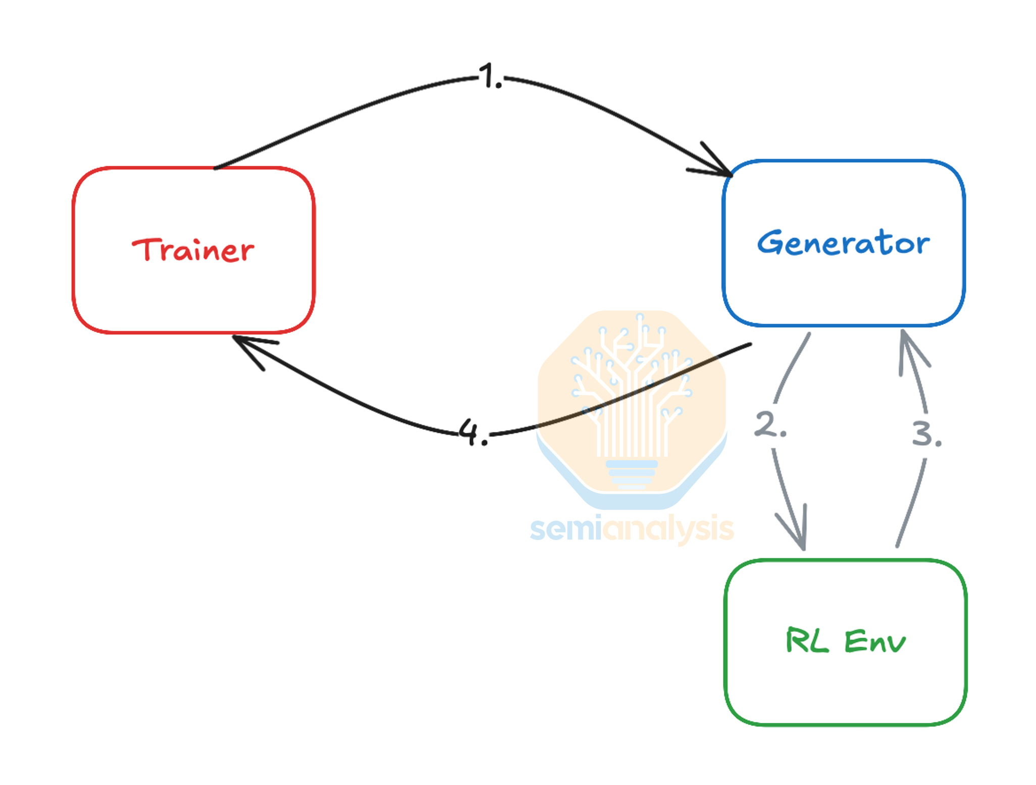
Use of Reinforcement Learning techniques for model improvement increases CPU demand further. From our deep dive on Reinforcement Learning, we see that in an RL training loop, the “RL Environment” needs to execute the actions generated by the model and calculate the appropriate reward. To do this in areas such as coding and mathematics, lots of CPUs are needed in parallel to perform code compilation, verification, interpretation, and tool use. CPUs are also heavily involved in complex physics simulations and verifying generated synthetic data at high precision. The growing complexity of RL environments needed to scale models further thus necessitates large high-performance CPU clusters located close to the main GPU clusters to keep them busy and minimize GPU idle time. This increasing reliance on RL and CPUs in the training loop is creating a new bottleneck, as AI accelerators are improving in Performance per Watt at a far greater rate than CPUs, meaning a future GPU generation such as Rubin may require an even higher ratio of CPU to GPU power than the 1:6 ratio seen in Fairwater above.

On the inference side, the rise of Retrieval Augmented Generative (RAG) models that search and use the internet along with agentic models that invoke tools and query databases has significantly increased the need for general-purpose CPU compute to service these requests. With the ability to send out API calls to multiple sources, each agent can essentially use the internet far more intensively than a human can by doing simple Google searches. AWS and Azure are doing massive CPU buildouts of their own Graviton and Cobalt lines of CPUs as well as purchasing even more x86 general purpose servers for this stepfold increase in internet traffic.
As we go through 2026, the demands on datacenter CPU and DRAM are only getting stronger. Frontier AI labs are running out of CPUs for their RL Training needs and are scrambling for CPU allocation by competing directly with the cloud providers for commodity x86 CPU servers. Intel, facing the unexpected depletion of their CPU inventory, is looking to raise prices across their Xeon line while they ramp additional tools to shore up CPU production. AMD has been increasing their supply capability to grow and take share in a server CPU TAM it believes will grow in the “strong double digits” in 2026. We will discuss how the CPU landscape evolves beyond 2026 for our subscribers below.
History of Multi-Core CPU Interconnects
To appreciate the design changes and philosophies of the 2026 CPUs, we have to understand how multi-core CPUs work and the evolution of interconnects as core counts grew. With multiple cores comes the need to connect those cores together. Early dual-core designs such as Intel’s Pentium D and Xeon Paxville in 2005 simply consisted of two independent single cores, with core-to-core communication done off-package via the Front Side Bus (FSB) to a Northbridge chip that also housed the memory controllers. AMD’s Athlon 64 X2, also in 2005, could be considered a true dual-core processor with two cores and an integrated memory controller (IMC) on the same die, allowing the cores to communicate with each other and to memory and IO controllers directly within the silicon through on-die NoC (Network on Chip) data fabrics.
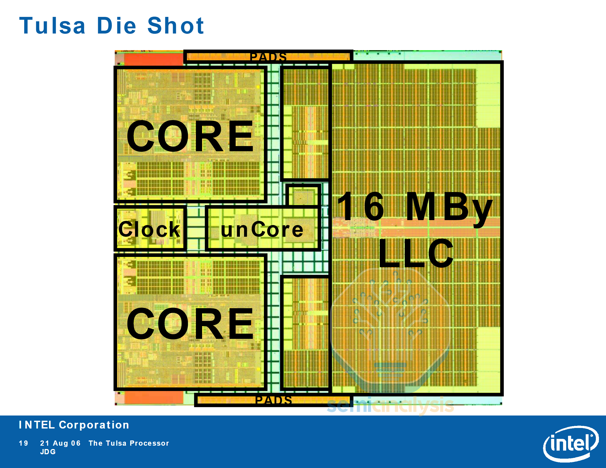
Intel’s subsequent Tulsa generation included 16MB of L3 cache shared between the two cores and functions as an on-die core to core data fabric. As we will see later, these on-die data fabrics will become a crucial factor in datacenter CPU design as core counts grow in the hundreds.
Crossbar Limits
As designers tried to increase core counts further, they ran into scaling limits of these early interconnects. As minimal latency and uniformity was desired, crossbar designs were used in an all-to-all fashion, where every core has a discrete link to all other cores on die. However, the number of links increased greatly with more cores, increasing complexity.
2 cores: 1 connection
4 cores: 6 connections
6 cores: 15 connections
8 cores: 28 connections
The practical limit for most designs ended at 4 cores, with higher core count processors achieved with multi-chip modules and dual-core modules that shared and L2 cache and data fabric socket between core pairs. The crossbar wiring is usually done in the metal lines above the shared L3 caches, saving area. Intel’s 6-core Dunnington in 2008 used three dual-core modules with 16MB of shared L3.
AMD launched their 6-core Istanbul in 2009 with a 6-way crossbar and 6MB L3. Their 12-core Magny-Cours in 2010 used two 6-core dies, with the 16-core Interlagos consisting of two dies each with four Bulldozer dual-core modules.
Intel’s Ring Bus
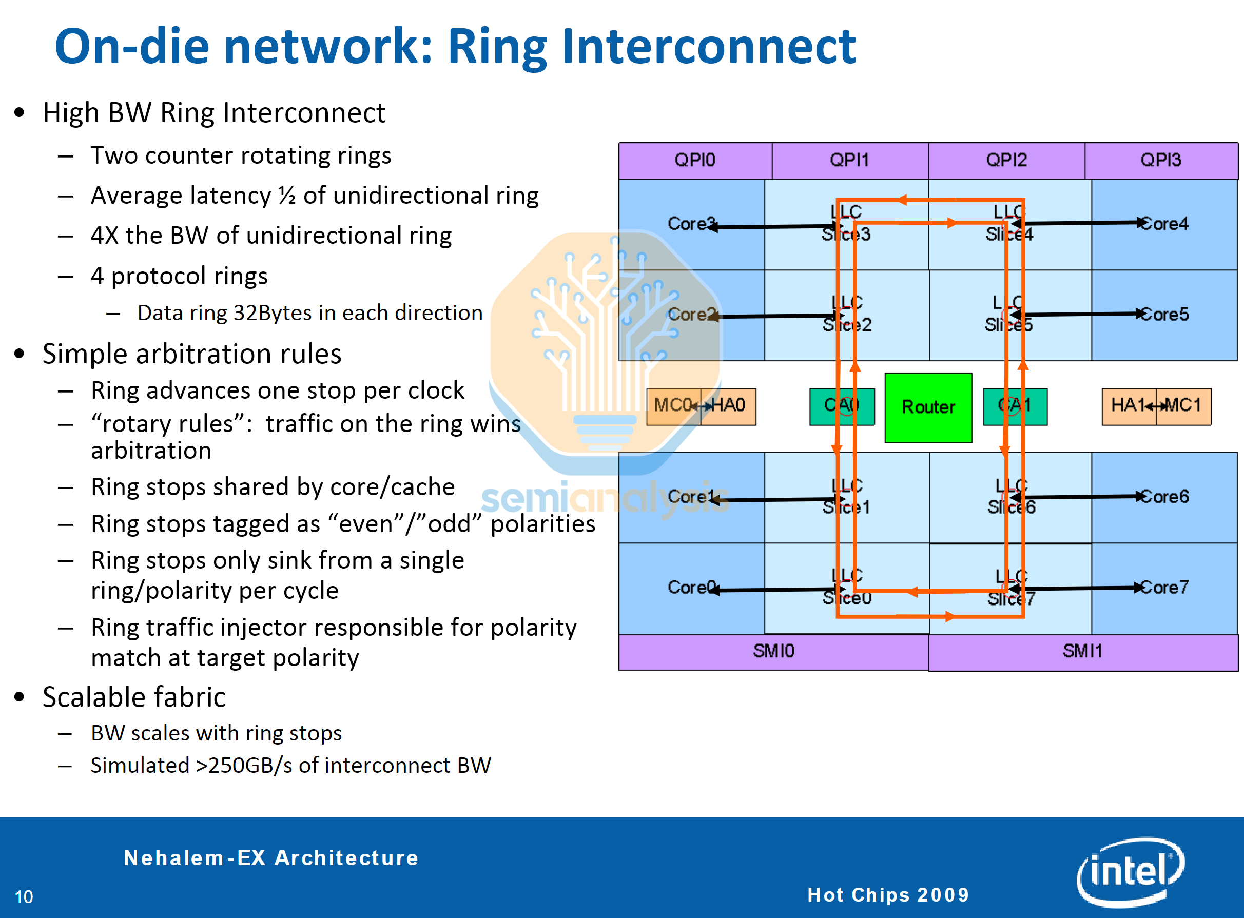
To scale past this limit, Intel implemented a ring bus architecture with their Nehalem-EX (Beckton) Xeons in 2010, bringing 8 cores with integrated memory controllers and inter-socket QPI links into a single die. Implemented in earlier years within ATi Radeon GPUs and the IBM Cell processor, the ring bus arranges all nodes into a loop, with ring stops integrated into the L3 cache slices and wiring in the metal layers above the cache. Caching and Home agents deal with memory snooping between cores and coherence with the memory controller.
Data from each ring stop’s core and L3 cache slice is queued and injected into the ring, with data advancing one stop per clock to its target destination. This means core to core access latency is no longer uniform, with cores on opposite sides of the ring having to wait additional cycles compared to directly adjacent cores. To help with latency and congestion, two counter rotating rings are implemented, with the optimal direction of travel chosen based on address and ring loading. With wiring complexity now moderated, Intel could scale core counts to 8 on Nehalem-EX and 10 for Westmere-EX. However, scaling beyond that with a single ring would lead to problems with coherence and latency as the ring gets too long.
Ivy Bridge-EX Virtual Rings
To scale core count to 15 for the Ivy Bridge generation, Intel had to get clever with the routing topology. The cores are arranged in three columns of five, with three ‘virtual rings’ looping around the columns. Switches in the ring stops controlled the direction of travel along the half rings, creating a “virtual” triple ring configuration.
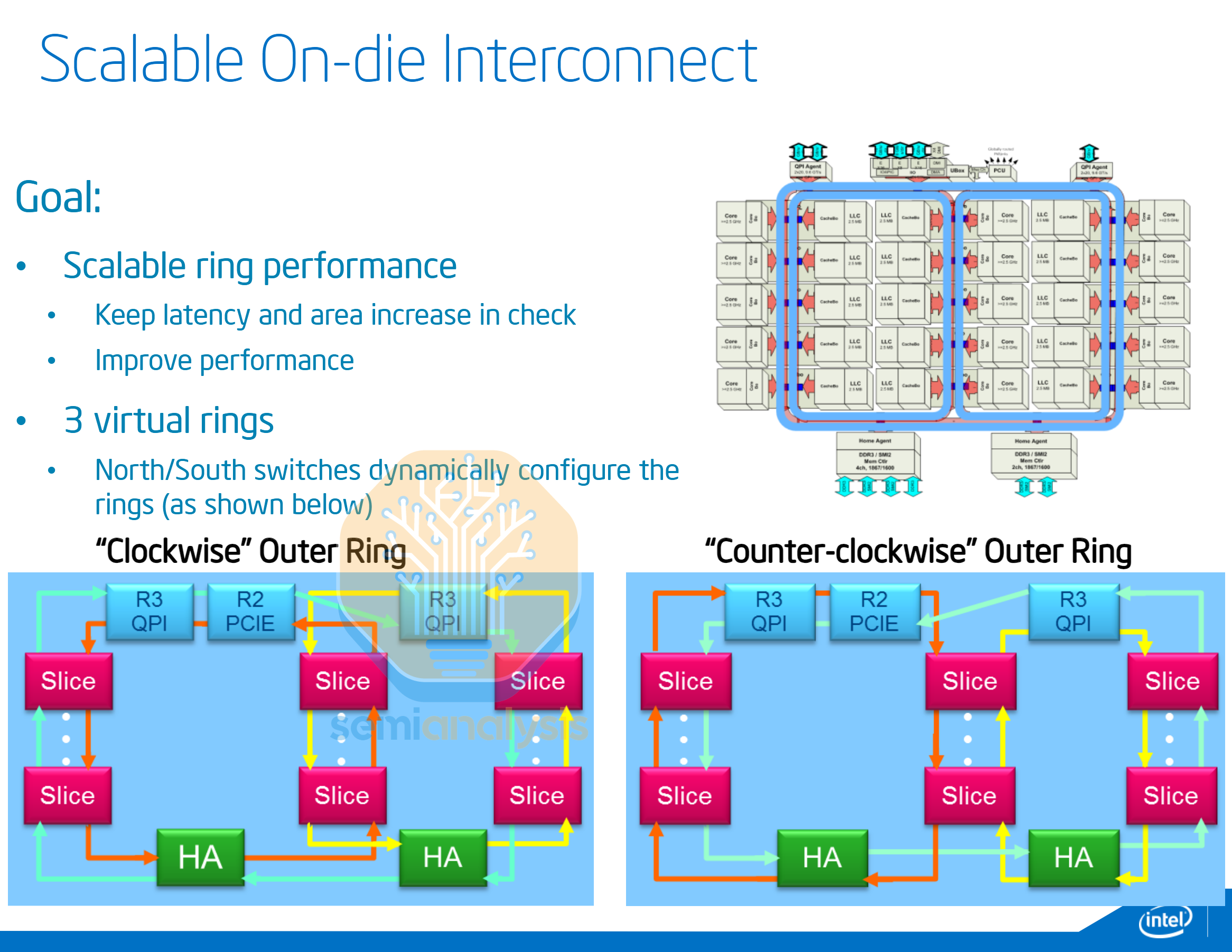
Haswell and Broadwell Dual Rings
In 2014, Intel changed topologies yet again with the 18-core Haswell HCC die featuring dual independent counter rotating ring buses connected with a pair of bi-directional buffered switches. Memory controllers were split amongst the two rings, with the 8-core ring also housing the IO ring stops. The MCC die variant wrapped a single half-ring back on itself. Broadwell HCC, released in 2015, brought core counts up to 24 with dual 12-core ring buses.
The downside to stitching multiple rings together is the increased variability in core to core and memory access latency, especially so when cores on one ring are accessing the memory of the other ring. This Non Uniform Memory Access (NUMA) was detrimental to system performance for programs that are latency sensitive with high core to core interactivity.
To help with this, Intel offered a “Cluster on Die” configuration option in the BIOS that treated the two rings as independent processors. The operating system would show the CPU being split into two NUMA nodes, each with direct access to half the local memory and L3 cache. Testing in CoD mode showed that latency within each ring stayed under 50ns while access to the other ring took over 100ns, illustrating the latency penalty of going through the buffered switches.
While these methods helped Intel increase core counts to 24, it was not an elegant nor scalable solution. Adding a third ring and two more sets of buffered switches would be too complicated and impractical, creating many NUMA clusters. A new interconnect architecture was required for more cores.
Intel’s Mesh Architecture
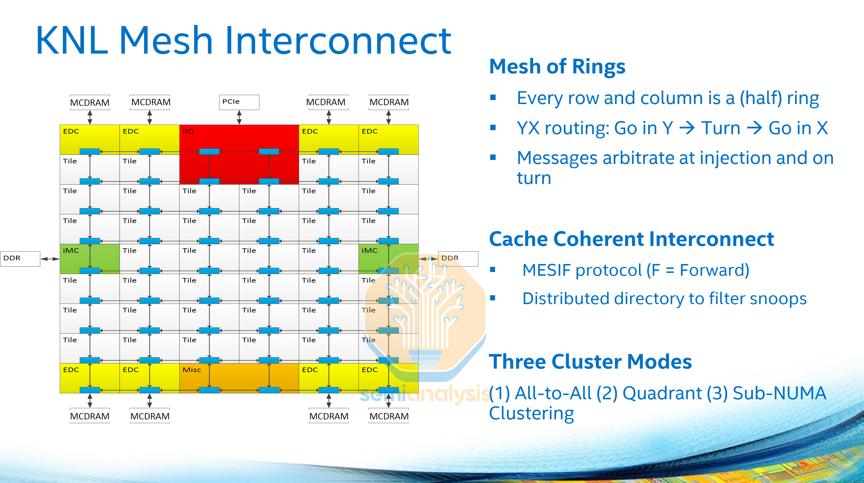
To solve the scalability problem, Intel adopted the mesh interconnect architecture used in their 2016 Xeon Phi “Knights Landing” processor for their mainline Skylake-X Xeon Scalable CPUs in 2017, bringing 28 cores in the XCC die. While core counts did not increase much over Broadwell, the design would form the base that would scale core counts over the next decade.
In a mesh architecture, cores are arranged in a grid, with each column and row connected with half rings, forming a 2D mesh array. Each mesh stop can house cores and L3 cache slices, PCIe IO, the IMC, and accelerators. Routing between cores is done in a circular manner, with data travelling in the vertical direction before moving horizontally across. The caching and home agents are now distributed across all the ring stops along with their snoop filters for memory coherence across the network.
With a mesh network and multiple memory controllers on opposite sides of the die, memory access and core to core latency would vary significantly with large meshes. As with the earlier Cluster on Die approach, several clustering modes were offered that split the mesh into quadrants for Sub-NUMA Clustering (SNC), reducing average latencies at the expense of treating each processor as multiple sockets with smaller L3 and memory access pools for each NUMA node.
In Knights Landing, each mesh stop housed two cores with a shared L2 cache. The mesh grid is 6 columns by 9 rows in size, with top and bottom rows more IO and MCDRAM. The mesh network runs on it’s own clock, and can dynamically adjust mesh clocks to save power. On Knights Landing, the mesh ran at 1.6GHz.
With Skylake-X, the 28 cores are arranged in a 6x6 mesh with a north IO cap and 2 spots for the IMC on the sides. The mesh array is smaller due to the size of the cores, which added more L2 cache and an AVX-512 extension to the core for increased floating point performance. The die size would exceed the 26 x 33 mm reticle limit if another row or column were to be added. With a smaller mesh and higher CPU frequencies of up to 4.5GHz, the mesh clock was increased to 2.4GHz, allowing similar average latencies to Broadwell’s dual rings.
The subsequent Cascade Lake and Cooper Lake processors brought minor changes with the same 28-core layout. As a side node, Intel made a 56-core dual die MCM in Cascade Lake-AP and cancelled a similar version for Cooper Lake CPX-4 in response to AMD’s datacenter return with EPYC.
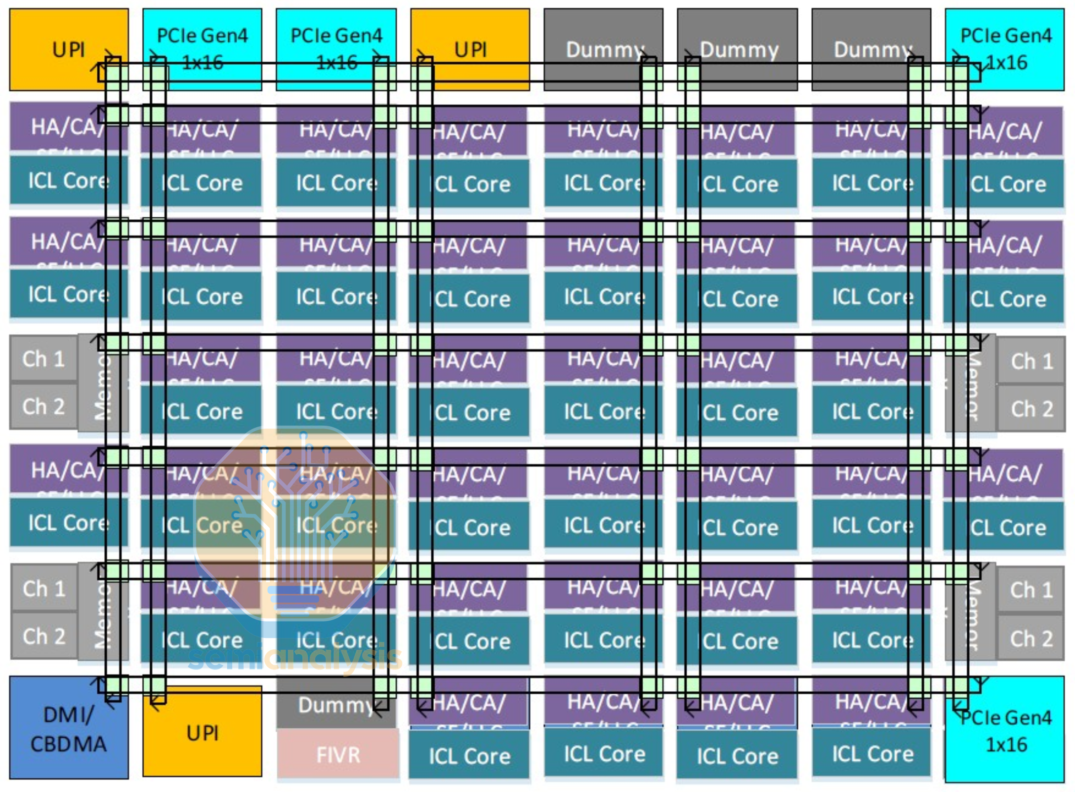
The next Ice Lake generation benefited from a node shrink from 14nm to 10nm, allowing core counts to increase to 40 cores in a 8x7 mesh, the maximum within the reticle limit. However, the next generation Sapphire Rapids was still going to be on the same node and with more features. That placed Intel in a pickle with how to increase core counts again.
Disaggregated Mesh Across EMIB
Sapphire Rapids added Advanced Matrix Extension (AMX) engines for matrix multiplication and AI, further increasing core area. That meant a single monolithic die would only fit 34 cores, a regression from Ice Lake. To increase core counts to 60, Intel had no choice but to split the cores across multiple dies again. However, they wanted to keep the silicon “logically monolithic”, such that the processor would appear and perform identically to a single die.
Thus, Sapphire Rapids debuted Intel’s EMIB advanced packaging technology to carry the mesh architecture across dies. Two pairs of mirrored 15-core dies were stitched together with a Modular Die Fabric, creating a much larger 8x12 mesh across four quadrants and nearly 1600 mm2 of silicon. A double row of mesh stops were required for the IO to facilitate the increased data traffic between the doubled throughput of PCIe 5.0 and the new data accelerator blocks.
With a much larger mesh spanning multiple dies, average core to core latencies deteriorated to 59ns from Skylake’s 47ns. To avoid using the mesh network as much as possible, Intel increased the private L2 cache for each core to 2MB, resulting in more L2 cache on die than L3 cache (120MB vs 112.5MB). Sub-NUMA Clustering (SNC) was also recommended more with each die treated as its own quadrant.
While a first for Intel in going to chiplets, Sapphire Rapids was infamous for its multi-year delay and numerous revisions. Perhaps due to performance problems getting the mesh to function across EMIB or from other execution issues, the final version made it all the way to stepping E5 before release in early 2023. Original roadmaps slated it for 2021.
The subsequent Emerald Rapids update in late 2023 kept the same core architecture and node, but reduced the die count to 2. With less silicon area spent on the EMIB die to die links, Intel were able to increase core counts from 60 to 66 (up to 64 enabled for yield) while also nearly tripling L3 cache to 320MB. We wrote more about the design decisions here.

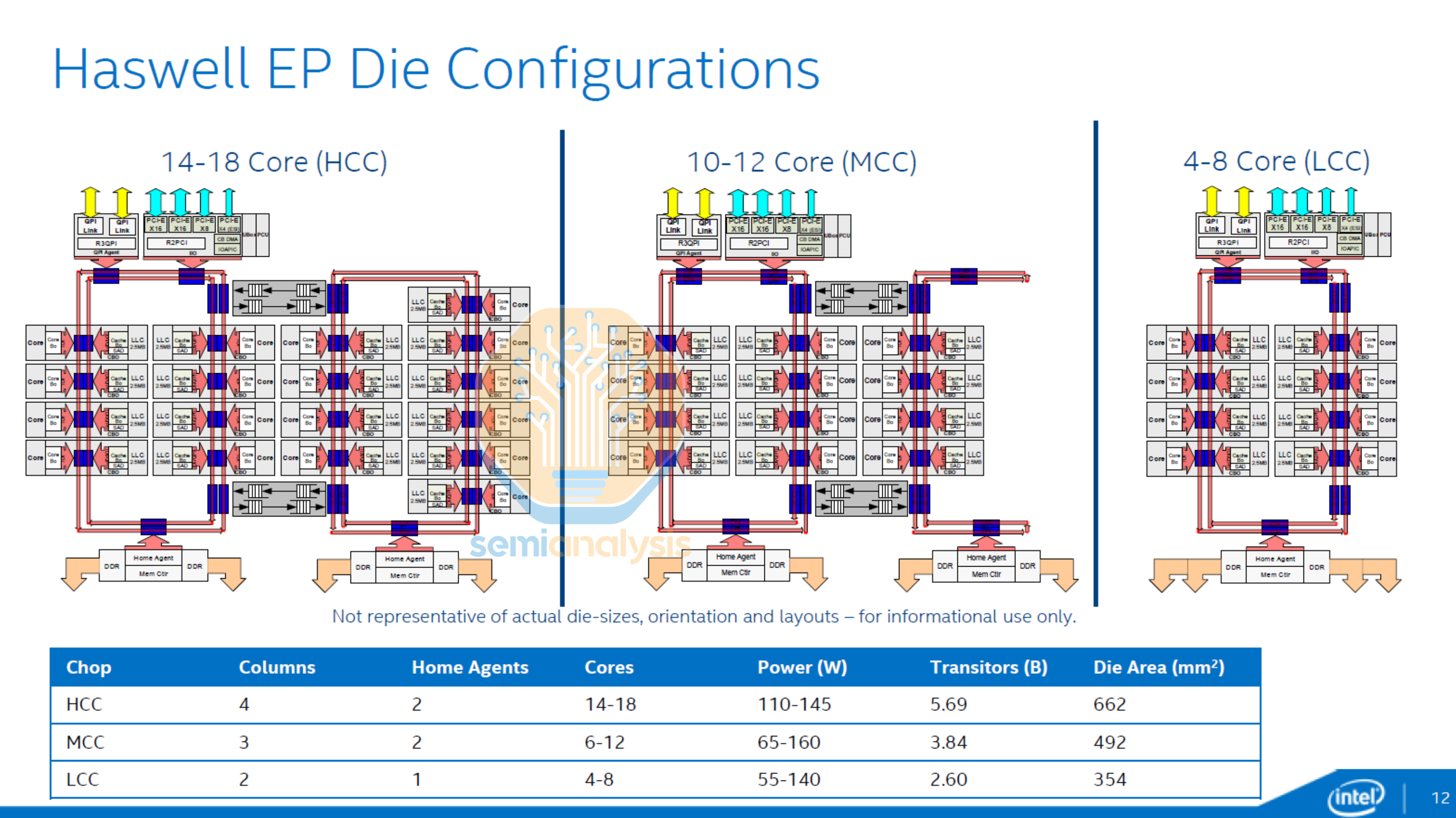
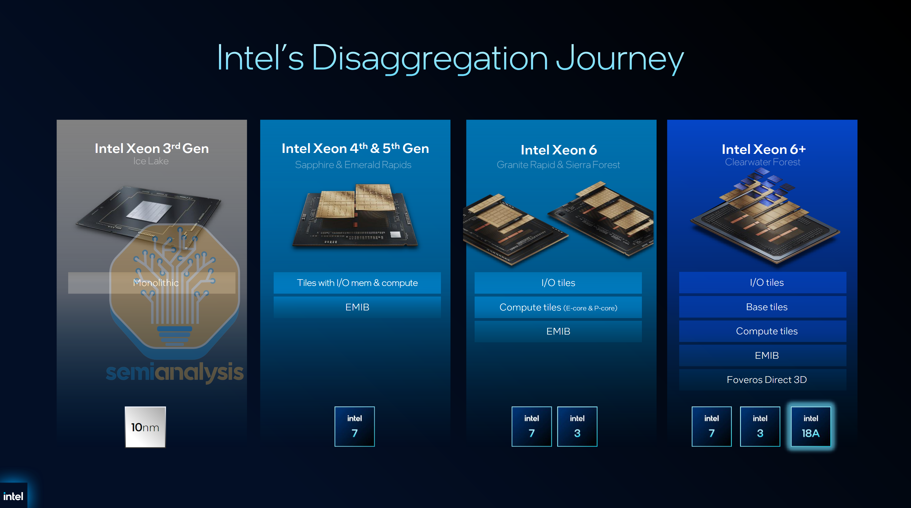
Heterogeneous Disaggregation on Xeon 6
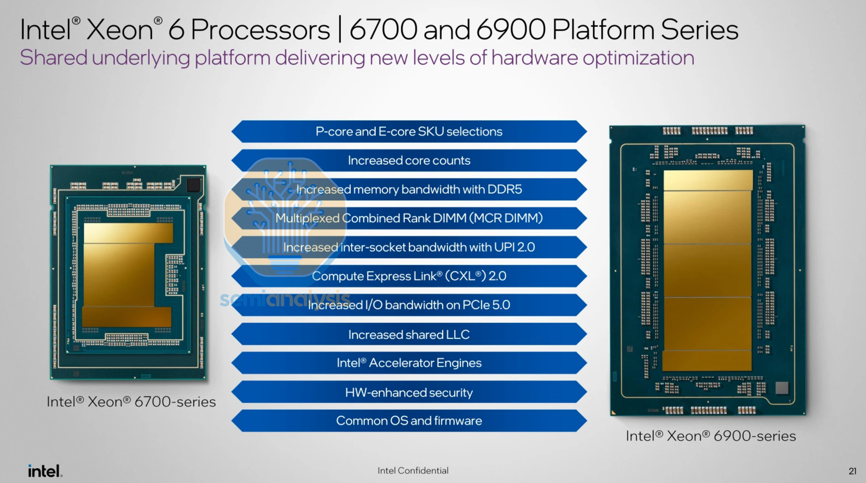
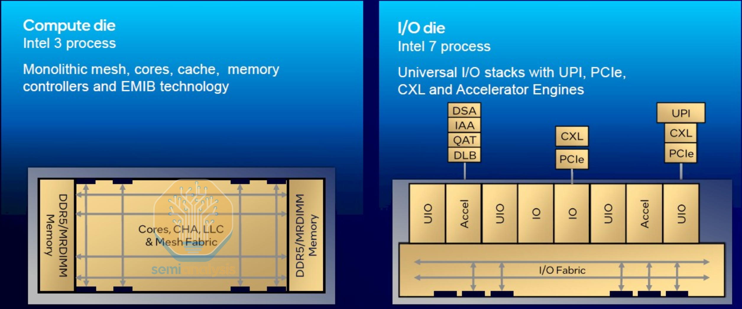
Another benefit going to a multi-die chiplet design beyond going past the reticle limit is being able to mix and match dies and share designs across different variants and configurations. For the next Xeon 6 platform in 2024, Intel went for heterogeneous disaggregation by partitioning the I/O away from the core and memory. Doing this allows the I/O dies to stay on the older Intel 7 node while the compute dies moved to Intel 3. Intel could thus reuse the I/O IP developed from Sapphire Rapids while saving cost as I/O does not benefit as much from moving to more advanced nodes. At the same time, the compute dies can be mixed and matched with both P-core Granite Rapids and E-core Sierra Forest configurations with up to 3 compute dies on the top Granite Rapids-AP Xeon 6900P series, creating a large 10x19 mesh over 5 dies, connecting 132 cores with up to 128 enabled for yield.
On the 144-core Sierra Forest, the E-cores are grouped into 4-core clusters that share a common mesh stop, arranged in an 8x6 mesh with 152 cores printed and up to 144 cores active. Although Sierra Forest was made on a request from hyperscalers for a “cloud-native” CPU with lower TCO per core, Intel has admitted that adoption has been limited, with hyperscalers already adopting AMD and designing their own ARM-based CPUs, while Intel’s traditional enterprise customers were not interested in it. As a result, the dual-die 288-core Sierra Forest-AP (Xeon 6900E) SKUs did not make it to general availability, surviving as low volume off-roadmap parts to serve the few hyperscale customers that ordered it.
Clearwater Forest Failure
The I/O dies are also being reused in the upcoming Xeon 6+ Clearwater Forest-AP E-core processors. The compute dies debut Intel’s Foveros Direct hybrid bonding technology, stacking 18A core dies atop base dies containing the mesh, L3 cache and memory interface, bringing core counts up to 288. Vertical disaggregation allows the compute cores to move to the latest 18A logic process while keeping the mesh, cache and I/O that does not scale as well on the older Intel 3 node.
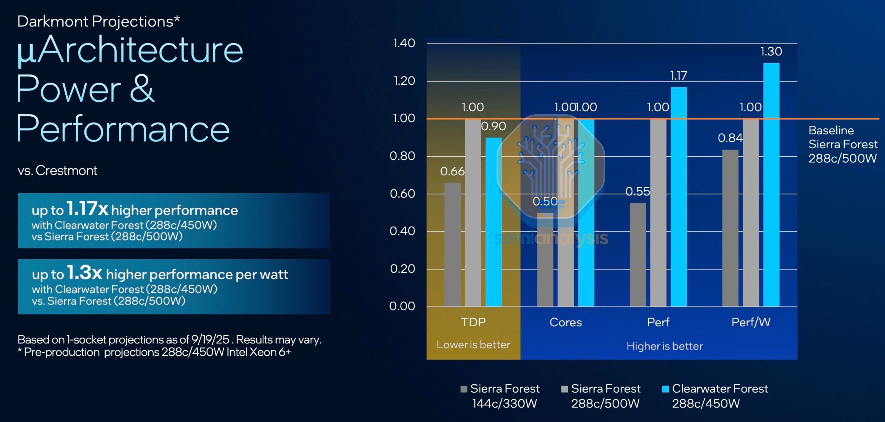
However, Intel’s execution issues surface again with Clearwater Forest, delaying availability from H2 ’25 to H1 ’26. Intel blamed the delay on their Foveros Direct integration challenges, which is not surprising with such a complex server chip being the lead vehicle as Intel tries to figure out hybrid bonding. Perhaps as a result of this, the vertically disaggregated interconnect has a relatively low bandwidth at only 35GB/s per 4-core cluster in accessing the base die’s L3 and mesh network.
Despite a two-year gap with new core micro-architecture, new node, new advanced packaging and higher cost, Intel showed Clearwater Forest as being only 17% faster than Sierra Forest at the same core counts. With such limited performance gains despite much higher costs from low hybrid bonding yields, it is no wonder that Intel barely mentioned Clearwater Forest in their latest Q4 ’25 earnings. Our take is that Intel does not want to produce these chips in high volumes which hurt margins and would rather keep this as a yield learning vehicle for Foveros Direct.
AMD’s Zen Interconnect Architecture
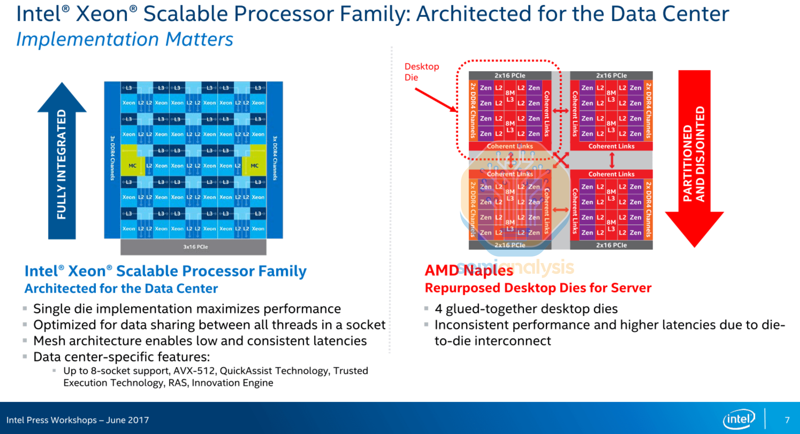
AMD’s return to the datacenter CPU market with their EPYC Naples 7001 series in 2017 caused quite a stir, with Intel mocking the design as “Four glued-together desktop die” with inconsistent performance. In reality, the small design team at AMD had to be resourceful, and could only afford to tape out a single die that had to be used for both desktop PCs, server and even embedded with integrated 10Gbit Ethernet on the same die.
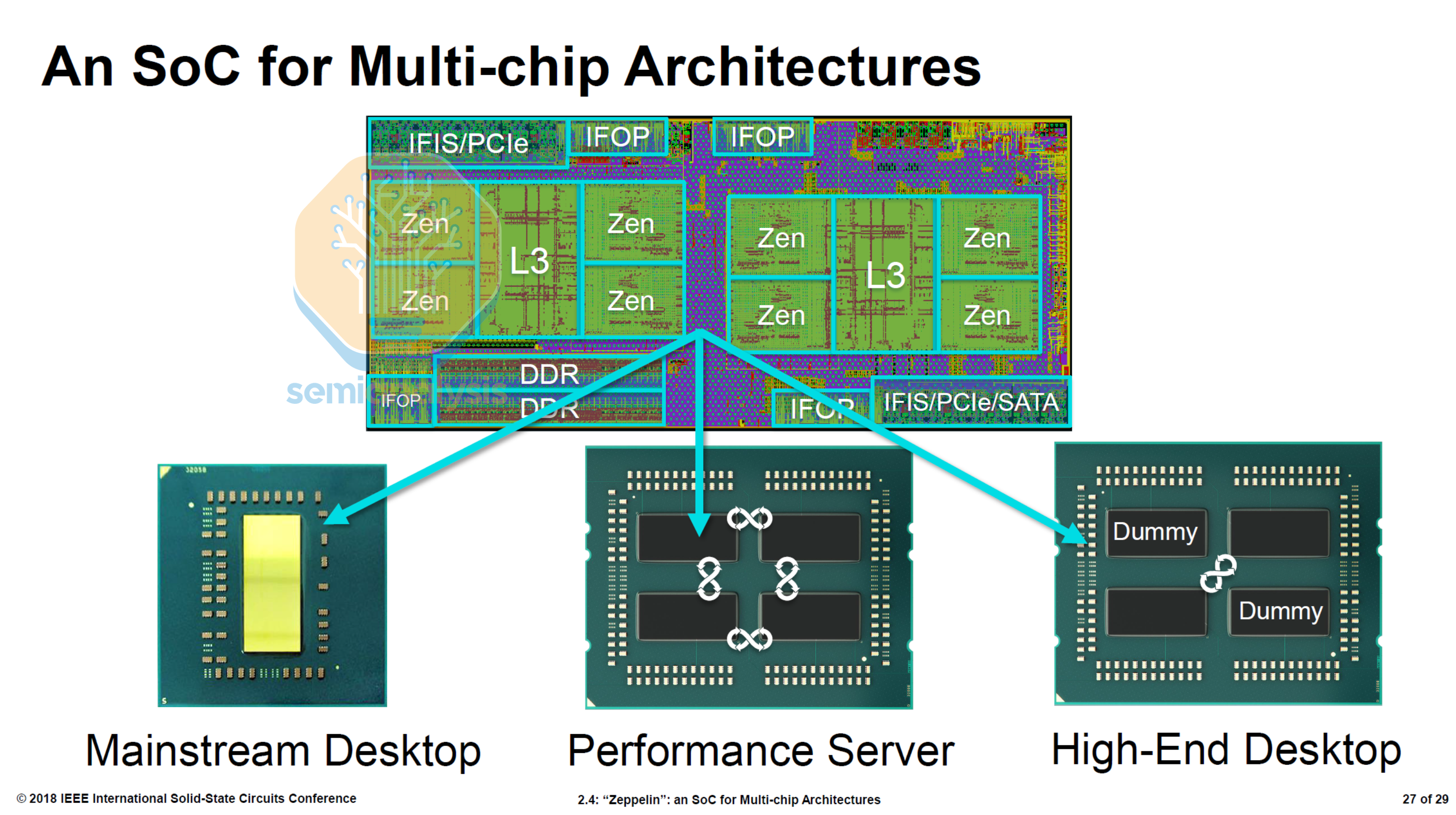
Naples implemented a 4-die MCM with each “Zeppelin” die containing 8 cores, allowing AMD to exceed Intel’s 28 cores with 32. Each die holds 2 Core Complexes (CCX), with 4 cores and 8MB of L3 connected with a crossbar. An on-die Scalable Data Fabric enables inter-CCX communication. Infinity Fabric on Package (IFOP) links connected each die to the other 3 in the package, while Infinity Fabric Inter Socket (IFIS) links enabled dual-socket designs. Infinity Fabric enabled coherent memory sharing between dies, and was derived from their old HyperTransport technology.
This architecture meant that there was no unified L3 cache and core-to-core latencies varied greatly, with multiple hops required to go from a core in a CCX on one die to a core in another die. A typical dual socket server ended having four NUMA domains. Intra-CCX, Inter-CCX, Die-to-die MCM, Inter-Socket. Performance reflected this, as highly parallelizable tasks with minimal core to core and memory access such as rendering performed well, while memory and latency sensitive tasks that relied more on inter-core communication did poorly. As most software was also not NUMA aware, this gave Intel’s criticism a point for “inconsistent performance”.
EPYC Rome’s Centralized IO
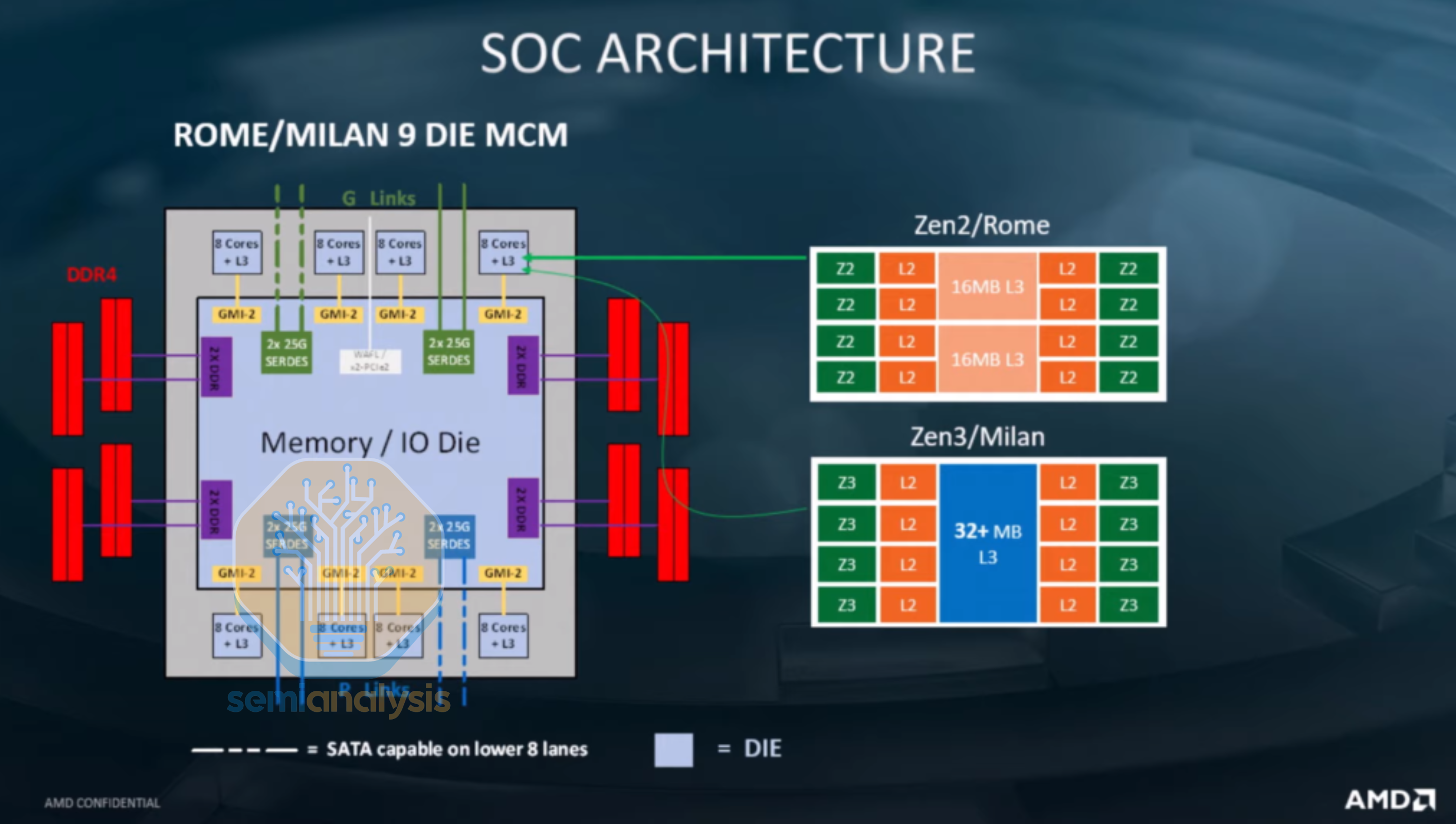
The 2019 Rome generation saw a complete rethink of the die layout, taking advantage of heterogeneous disaggregation to create a 64-core part that far outstripped Intel who were still stuck at 28. Eight 8-core Core Compute Dies (CCD) surrounded a central I/O die containing the memory and PCIe interfaces, with the CCDs moving to the latest TSMC N7 process while the I/O die stayed on GlobalFoundries’ 12nm. The CCDs still consisted of two 4-core CCXs, but now have no direct communication with each other. Instead, all inter-CCX traffic is routed through the I/O die, where signals travel across the substrate over Global Memory Interconnect (GMI) links. This meant that Rome functionally appeared as sixteen 4-core NUMA nodes with only 2 NUMA domains.
VMs spun up on Rome had to be kept to 4 cores to avoid performance loss from cross-die communications, much like the prior Naples. This was addressed with the Milan generation in 2021 that increased CCX size to 8 cores by moving to a ring bus architecture, while reusing the same I/O die as Rome.
Despite initial plans to adopt advanced packaging, AMD stuck to this familiar design for the next 2 generations as well, with 2022 Genoa moving to 12 CCDs and 2024 Turin with up to 16 CCDs on the 128-core EPYC 9755, all surrounding a central I/O die with upgraded DDR5 and PCIe5 interfaces.
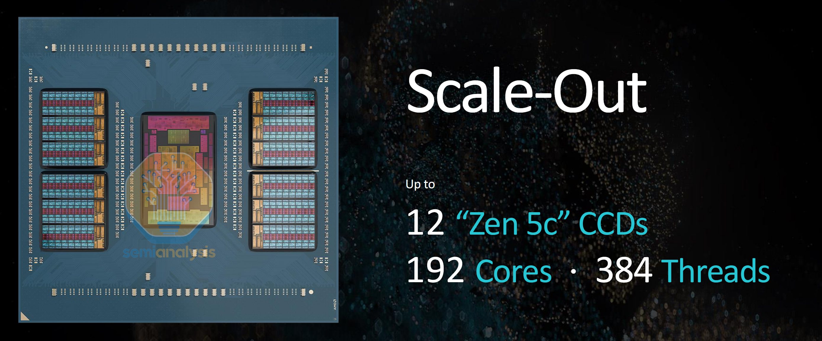
The key benefit of this chiplet design is the scalability of core counts with just a single silicon tapeout. AMD only needs to design a single CCD to offer the full gamut of core counts across the SKU stack by including different numbers of CCDs. The small die area of each CCD also helps with yields and achieving earlier time to market when moving to a new process node. This contrasts with a mesh design that uses large reticle sized dies and requires multiple tapeouts for each core count offering with smaller meshes. Different CCD designs can also be swapped in while sharing the same IO die and socket platform, with AMD creating additional variants using the compact Zen 4c cores in Bergamo and Zen 5c cores for the 192-core Turin variant. We wrote about this new core variant for efficient cloud computing here. Disaggregation also allows smaller versions to be made with EPYC 8004 Siena processors using just 4 Zen 4c CCDs on a 6-channel memory platform.

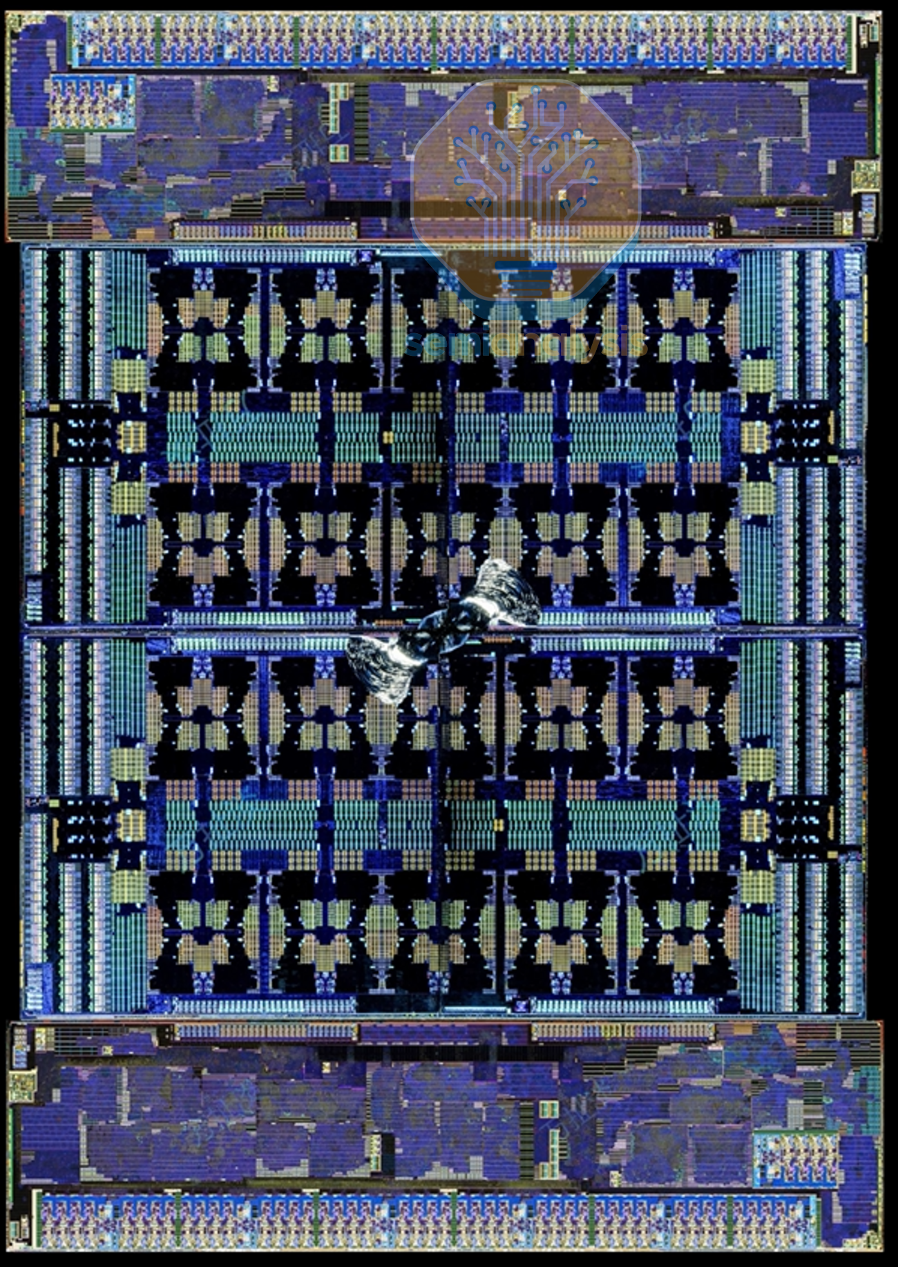
Intel Diamond Rapids Architecture Changes
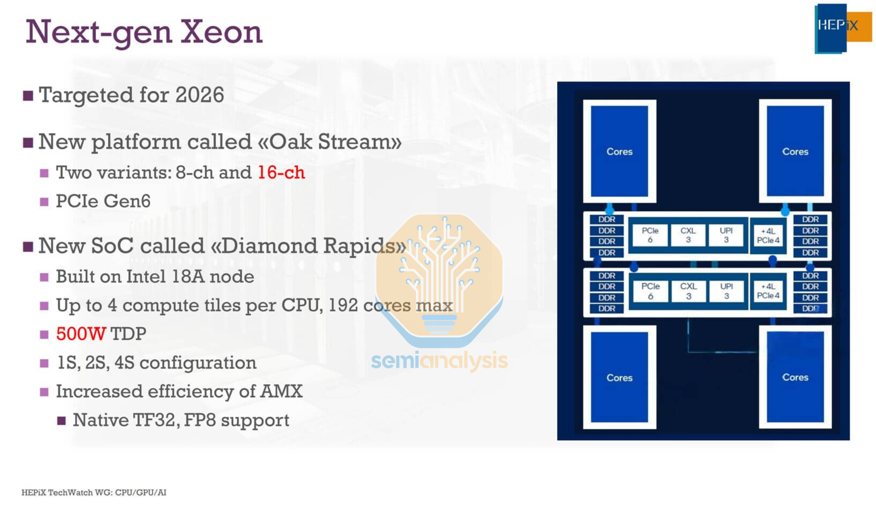
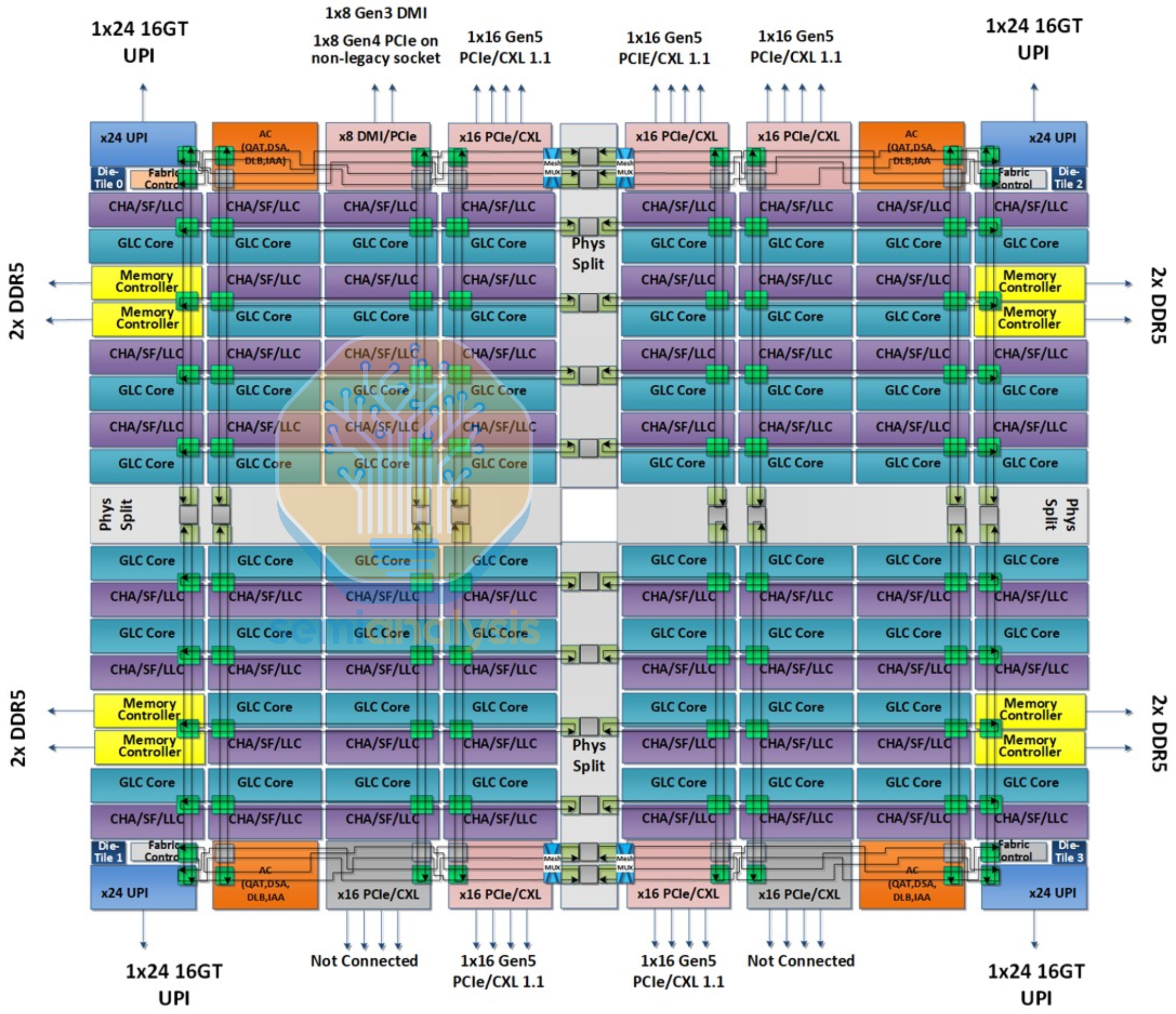
At first glance, Diamond Rapids almost looks like a copy of AMD’s designs, with compute dies surrounding a central I/O die. It seems that it was too difficult to grow a single mesh network beyond the 10x19 on Granite Rapids to further increase core count, meaning Intel finally succumbs to having multiple NUMA nodes and L3 domains. Four Core Building Block (CBB) dies flank two I/O and Memory Hub (IMH) dies in the middle.
Within each CBB, 32 Dual Core Modules (DCM) on Intel 18A-P are hybrid bonded onto a base Intel 3-PT die containing the L3 cache and local mesh interconnect. To reduce the number of mesh stops and reduce network traffic, two cores now share a common L2 cache in each DCM, a design reminiscent of the Dunnington generation from 2008. While this means Diamond Rapids has 256 cores in total, it seems only up to 192 cores will be enabled for the mainline SKUs, with higher core counts presumably reserved for off-roadmap orders due to lower yields.
The IMH dies contain the 16-channel DDR5 memory interfaces, PCIe6 with CXL3 support, and Intel datapath Accelerators (QAT, DLB, IAA, DSA).
Interestingly, it seems that the die to die interconnect no longer requires EMIB advanced packaging, with long traces across the package substrate connecting each CBB die to both IMH dies, allowing each CBB direct access to the entire memory and IO interface without needing a second extra hop to the other IMH. This also ensures that only 2 cross-die hops are needed for any inter-CBB communication. As a result of moving away from advanced packaging and splitting the cores across 4 dies, we expect cross-CBB latencies to be appreciably worse off, with a large difference in latency compared to staying within the same die.
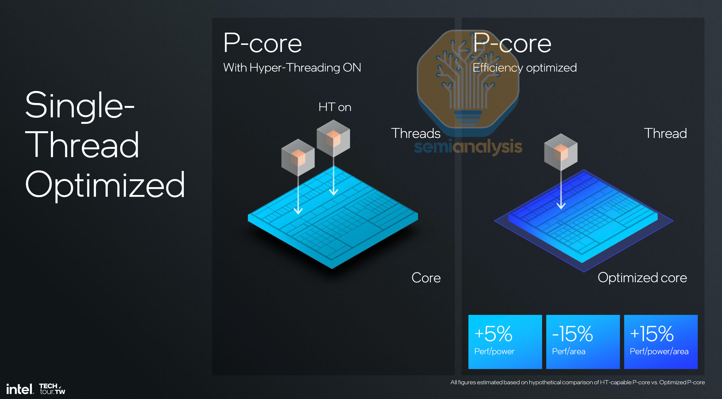
Though worse latencies are problematic, the worst issue with Diamond Rapids is the lack of SMT. Spooked by the Spectre and Meltdown vulnerabilities that fundamentally affected Intel more than AMD, their core design team began designing P-cores without it, starting with Lion Cove in the 2024 client PC. Intel rationalized it at the time by claiming the area saved by removing SMT functionality would give better efficiency at the expense of raw throughput. This was fine for PC designs as they had integrated E-cores alongside that would help bolster multi-threaded performance.
However, maximum throughput matters for datacenter CPUs, severely handicapping Diamond Rapids. Compared to the current 128 core, 256 thread Granite Rapids, we expect the main 192 core, 192 thread Diamond Rapids to be only around 40% faster, exposing Intel for another generation with lower performance than AMD.
In a late move, Intel has cancelled the mainstream 8-channel Diamond Rapids-SP platform entirely, leaving their highest volume core market without a new generation into at least 2028. While this helps streamline Intel’s bloated SKU stack, we feel this is the wrong move as general purpose compute for AI tool use and context storage uses more mainstream CPUs with good connectivity as opposed to massive performance per socket options.
AMD Venice Architecture Changes
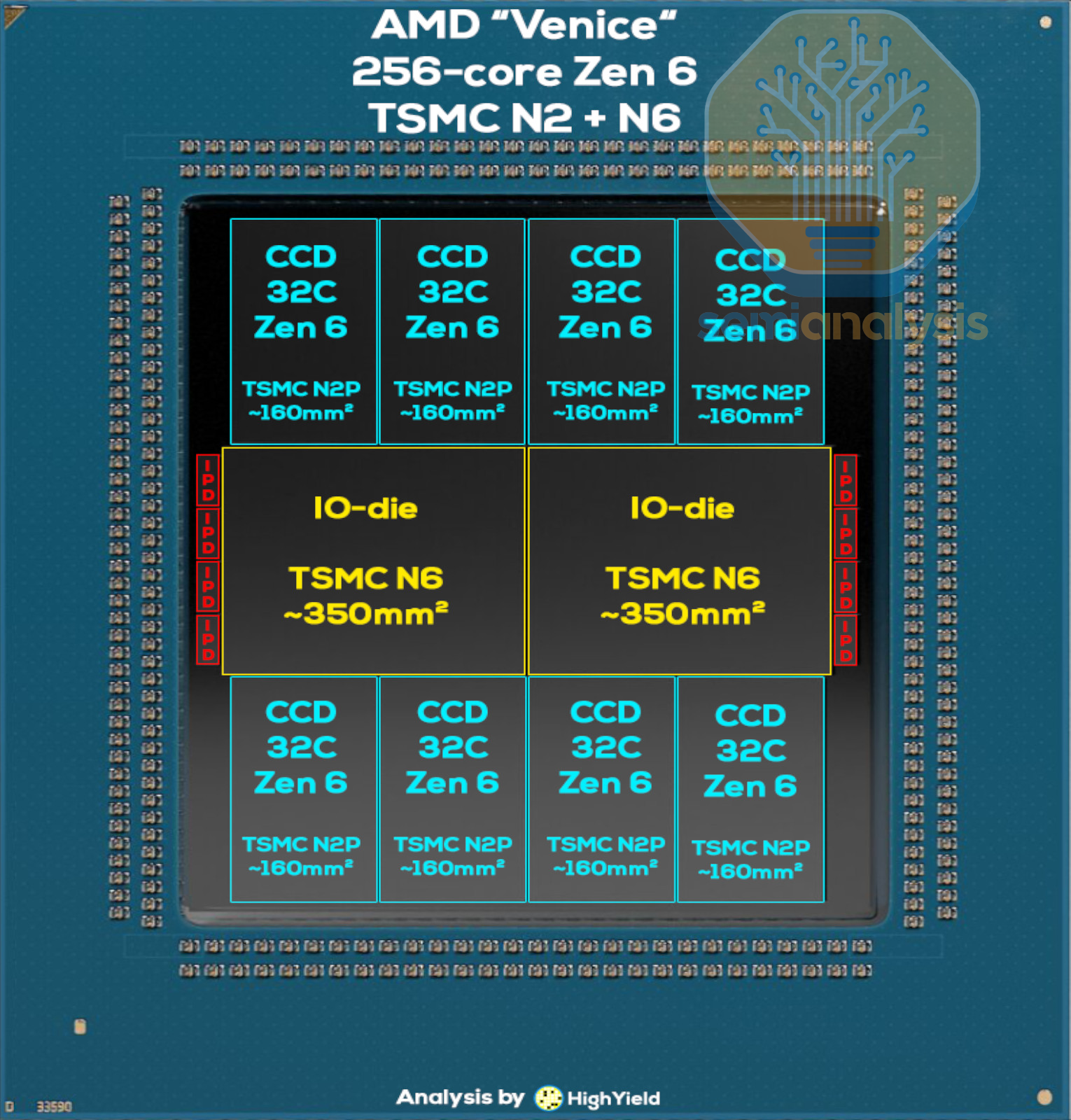
While Intel went away from EMIB, AMD finally adopts the equivalent advanced packaging technology for Venice, with high-speed short reach links connecting the CCDs to the I/O die. We have the volumes for this in our Accelerator, HBM, and Advanced Packaging Model.
The additional shoreline required for the CCD links takes up additional width, necessitating the central I/O hub to be split into 2 dies. This creates another die to die hop to cross the different halves of the chip, forming another NUMA domain that Intel’s solution avoids. The I/O dies now feature 16 memory channels in total, up from 12 in 2022’s Genoa. AMD also catches up to Intel in finally supporting Multiplexed memory for higher bandwidth, where 16-channel MRDIMM-12800 gives 1.64TB/s, 2.67x Turin.
AMD has also moved to a mesh network within the CCD, with 32 Zen6c cores in a 4x8 grid, although there may be an additional spare core included for yield recovery. Eight TSMC N2 CCDs bring core counts to 256, a one-third increase from the 192-core Turin-Dense 3nm EPYC 9965. Zen6c receives the full 4MB L3 cache per core that was previously halved on Zen5c, creating large 128MB cache regions per CCD.
Lower core count and frequency optimized “-F” SKUs for AI head nodes will employ the same 12-core Zen6 CCD design used in their consumer desktop and mobile PC line for up to 96 cores across 8 CCDs. While this is a regression from the 128-core Turin-Classic 4nm EPYC 9755, it does bring 50% more cores than the high frequency 64-core EPYC 9575F.
Lastly, 8 small dies can be seen beside the I/O dies next to where the DDR5 interface exits. These are Integrated Passive Devices (IPD) that help smooth power delivery to the chip in the heavily I/O dense area, where the SP7 package routing is saturated with memory channel fanout.
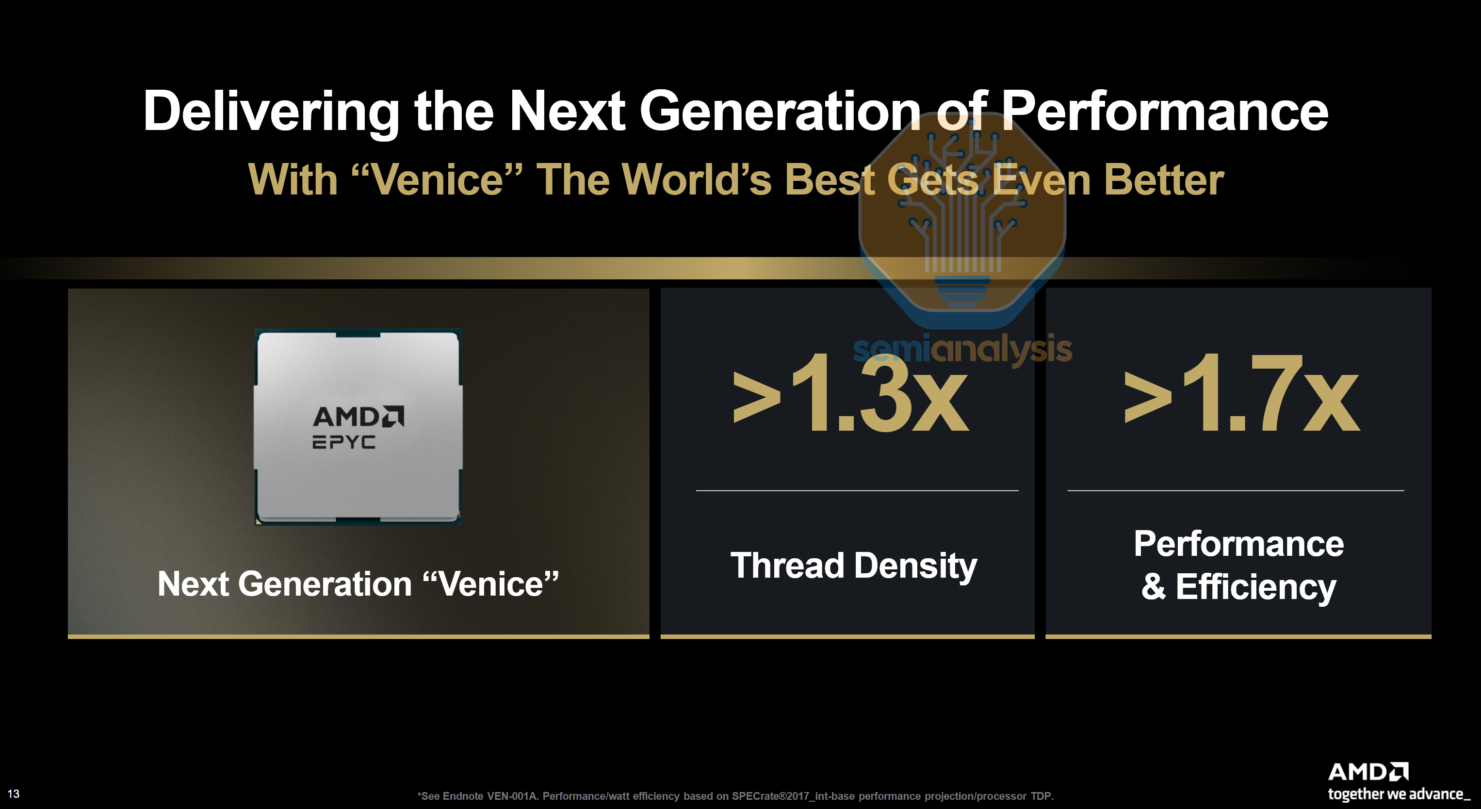
On the performance front, AMD claims the top 256-core variant is over 1.7x better in performance per watt than the top 192-core Turin in SPECrate®2017_int_base, meaning an even higher performance per core thanks to the new Zen 6 core microarchitecture with higher Instructions per Clock (IPC). Zen 6 also introduces new instructions for AI datatypes including AVX512_FP16, AVX_VVNI_INT8 and a new AVX512_BMM instruction for Bit Matrix Multiplication and bit reversal operations on the CPU’s floating point unit.
For BMM, the FPU registers store 16x16 binary matrices and computes BMM accumulates using OR and XOR operations. Binary matrices are far easier to compute than floating point matrices, and could offer large efficiency gains for software that can make use of it such as Verilog simulations. However, BMMs do not have sufficient precision for LLMs, and so we believe adoption of this instruction will be limited.
As AMD already enjoys significantly higher performance per core than Intel (96c Turin matches 128c Granite Rapids), the performance gap between AMD Venice and Intel Diamond Rapids will widen even more in the 2026 to 2028 generation of datacenter CPUs. Core to core latency on Venice should improve over Turin thanks to the new die to die interconnect and larger core domains.
AMD is also doubling down where Intel is pulling out. While Intel cancels its 8-channel processor, AMD will introduce a new 8-channel Venice SP8 platform as a successor to the EPYC 8004 Siena line of low power, smaller socket offerings, while still bringing up to 128 dense Zen 6c cores to the table. With this, AMD will see large share gains in the enterprise markets, a traditional Intel stronghold.
2026 CPU Costing Analysis
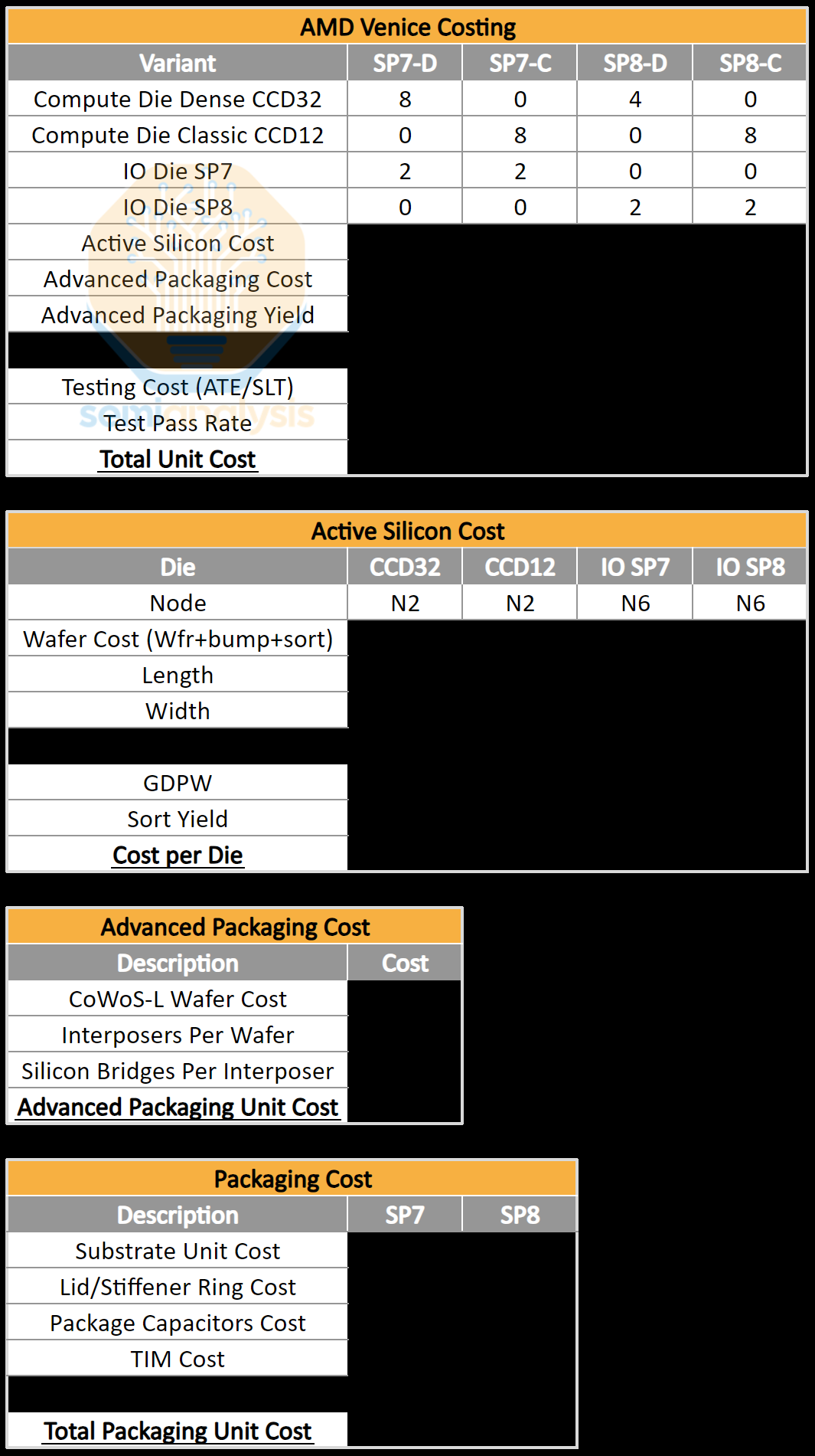
SemiAnalysis offers detailed Bill of Materials costing based on our extensive knowledge of the supply chain. To understand exact die sizes, configurations, topologies, performance estimates and competitiveness with Hyperscaler ARM CPUs, please contact us at Sales@SemiAnalysis.com for bespoke consulting and competitive analysis services. We have detailed costing and breakdowns of AMD Turin, Venice, Intel Granite Rapids, Diamond Rapids, NVIDIA Grace, Vera and hyperscale ARM CPUs from AWS, Microsoft, Google and more.
Nvidia Grace
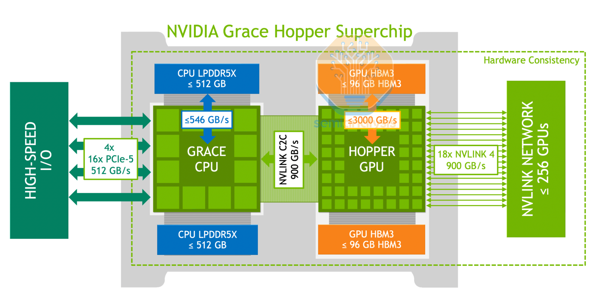
Unlike most of the general purpose CPUs covered in this article, Nvidia’s CPUs are designed with head nodes and Extended GPU Memory in mind, with NVLink-C2C as its party trick. This 900GB/s (bi-directional) high speed link allows the connected Hopper or Blackwell GPU to access the CPU’s memory at full bandwidth, alleviating the low memory capacity limits of HBM with up to 480GB memory per Grace CPU. Grace also adopts mobile-class LPDDR5X memory to keep non-GPU power down while maintaining high bandwidths of 500GB/s on a 512-bit wide memory bus. The initial Grace Hopper superchips attached 1 Grace for each GPU, while the later Grace Blackwell generations shared the CPU across 2 GPUs. NVIDIA also offered a dual-Grace superchip CPU for HPC customers that require high memory bandwidth.
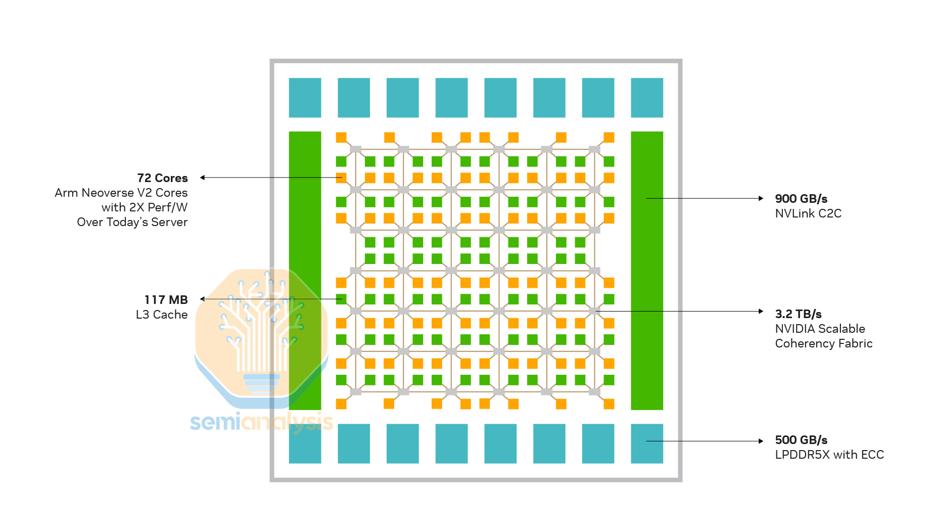
Regarding the CPU cores, NVIDIA uses the high performance ARM Neoverse V2 design with 1MB of private L2 cache on a 6x7 mesh network housing 76 cores and 117MB of L3 cache, with up to 72 cores enabled for yield. Each Cache Switch Node (CSN) on the mesh stop connects up to 2 cores and L3 slices. NVIDIA emphasizes the high 3.2TB/s bisection bandwidth of the mesh network, showing Grace’s specialized focus on data flow rather than raw CPU performance.
On the performance side, Grace has a quirky microarchitectural bottleneck from the Neoverse V2 cores that makes it slow for unoptimized HPC code. From Nvidia’s Grace Performance Tuning Guide, optimizing large applications for better code locality can result in 50% speedups. This is due to limitations in the core branch prediction engine in storing and fetching instructions ahead of use. On Grace, instructions are organized into 32 2MB virtual address spaces.
Performance starts to drop off massively when this Branch Target Buffer fills beyond 24 regions as hot code hogs the buffer and increases instruction churn, causing more branch prediction mispredicts. If the program exceeds 32 regions, the entire 64MB buffer gets flushed, with the branch predictor forgetting all previous branch instructions to accommodate new incoming ones. Without a functioning branch predictor, the CPU core’s front end bottlenecks the whole operating as ALUs sit idle awaiting instructions to execute.
This is why AI workloads are currently being slowed by the Grace CPUs in GB200 and GB300.
Nvidia Vera
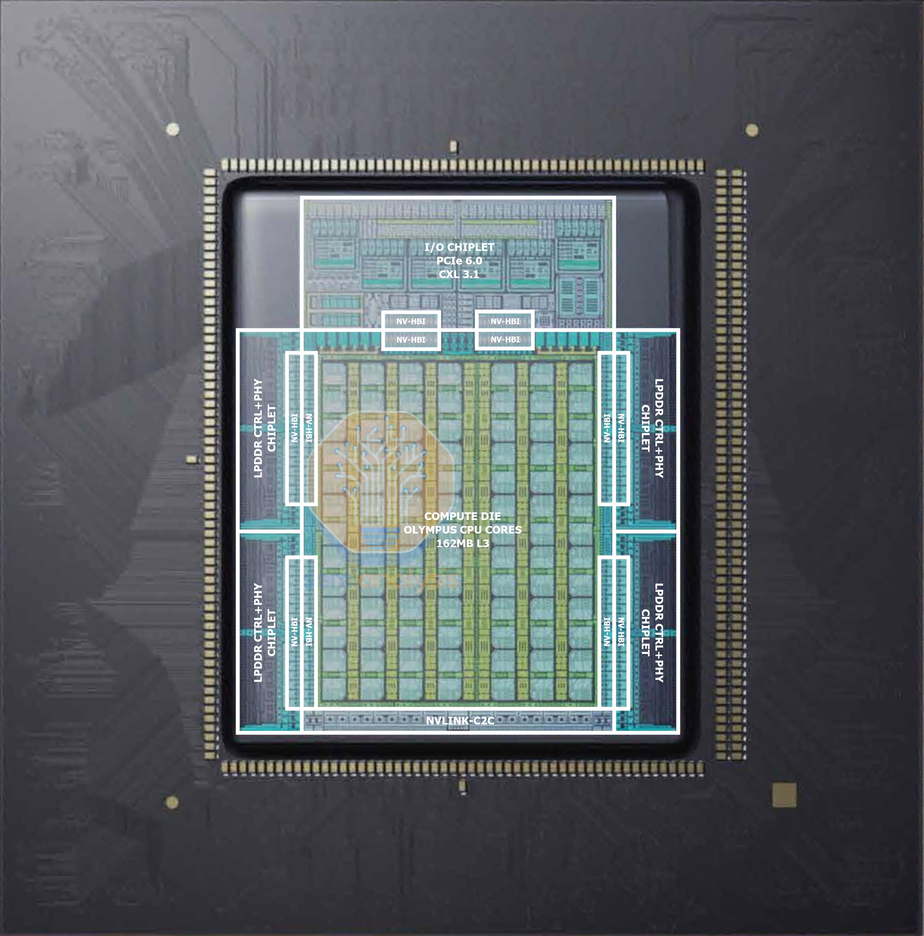
Vera takes things further in 2026 for the Rubin platform, doubling C2C bandwidth to 1.8TB/s and doubling the memory width with eight 128bit wide SOCAMM 192GB modules for 1.5TB of memory at 1.2TB/s of bandwidth. The mesh design remains, with a 7x13 grid that houses 91 cores, with up to 88 active. L3 cache increases to 162MB. NVIDIA now disaggregates the perimeter memory and I/O regions into separate chiplets, totaling 6 dies packaged with CoWoS-R (1 reticle-sized compute die on 3nm with NVLink-C2C, 4 LPDDR5 memory dies and 1 PCIe6/CXL3 IO die).
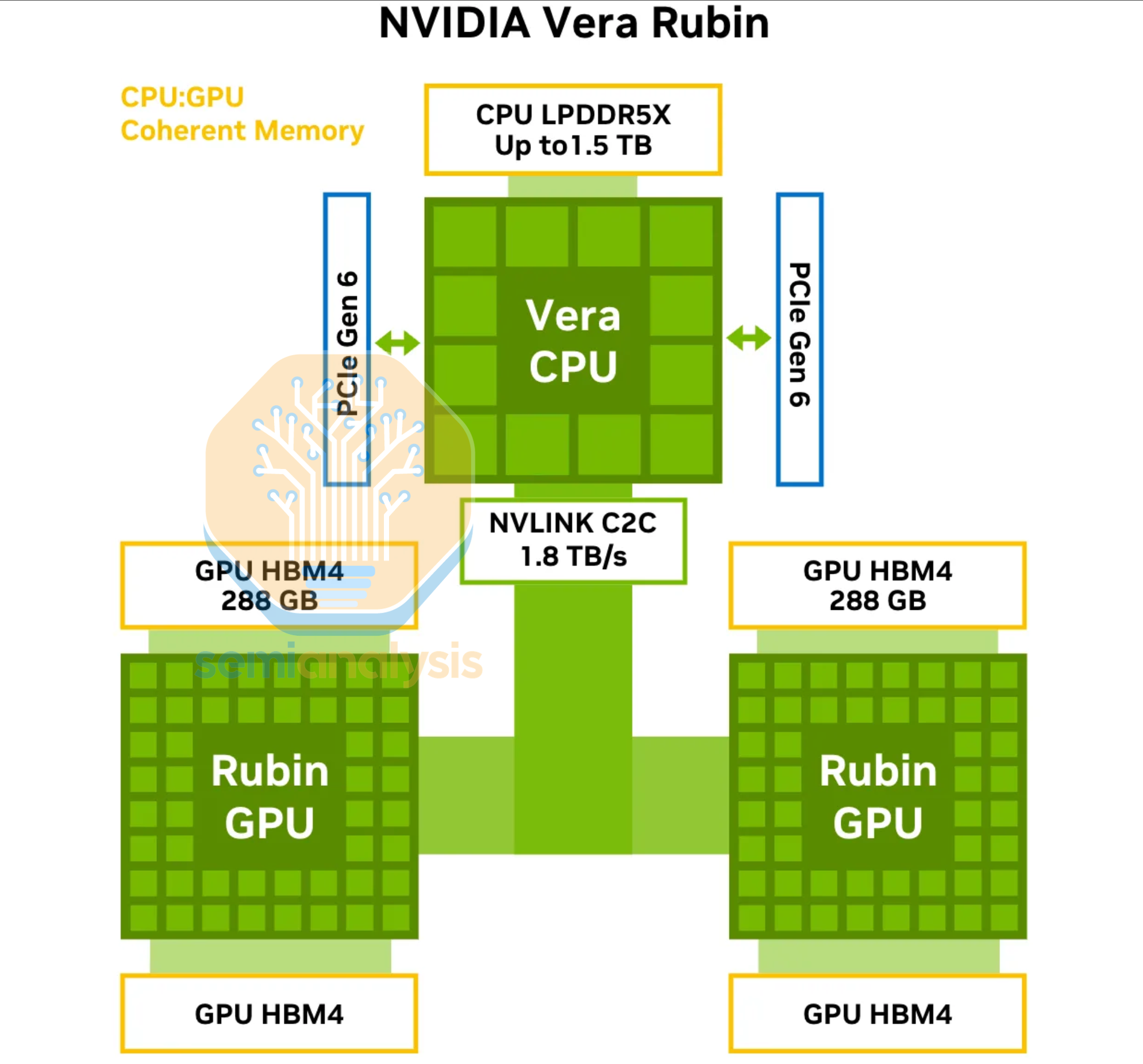
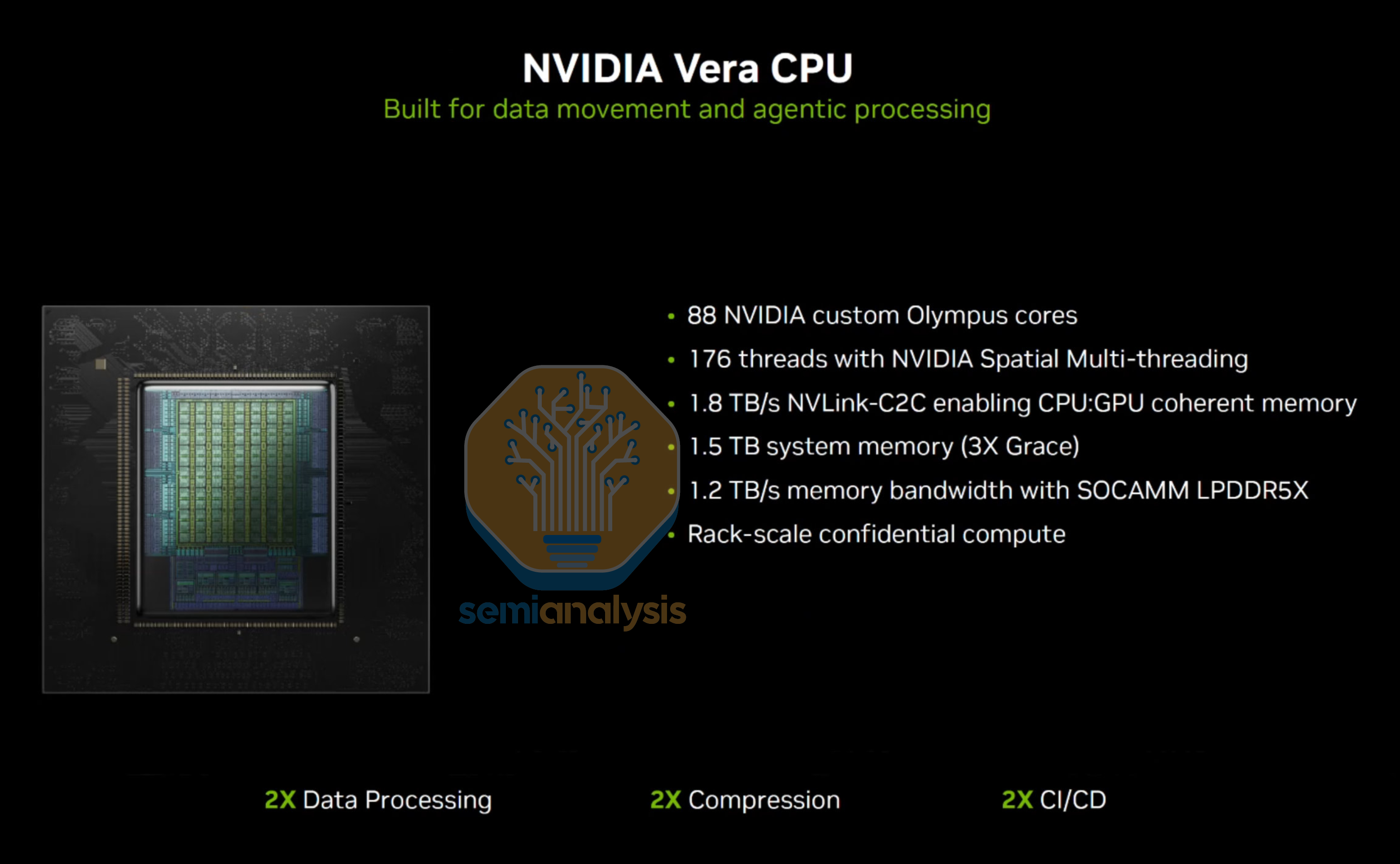
Perhaps burned by the performance bottlenecks of ARM’s Neoverse cores, NVIDIA has brought back their custom ARM core design team with a new Olympus core that supports SMT, enabling 88 cores with 176 threads. The last NVIDIA custom core was 8 years ago in the Tegra Xavier SoC with 10-wide Carmel cores. The ARMv9.2 Olympus core increases the width of the floating point unit to 6x 128b-wide ports vs 4 on Neoverse V2, now supporting ARM’s SVE2 FP8 operations. 2MB of private L2 cache supports each core, doubled from Grace. In total, Nvidia claims a 2x performance improvement going to Vera.
AWS Graviton5
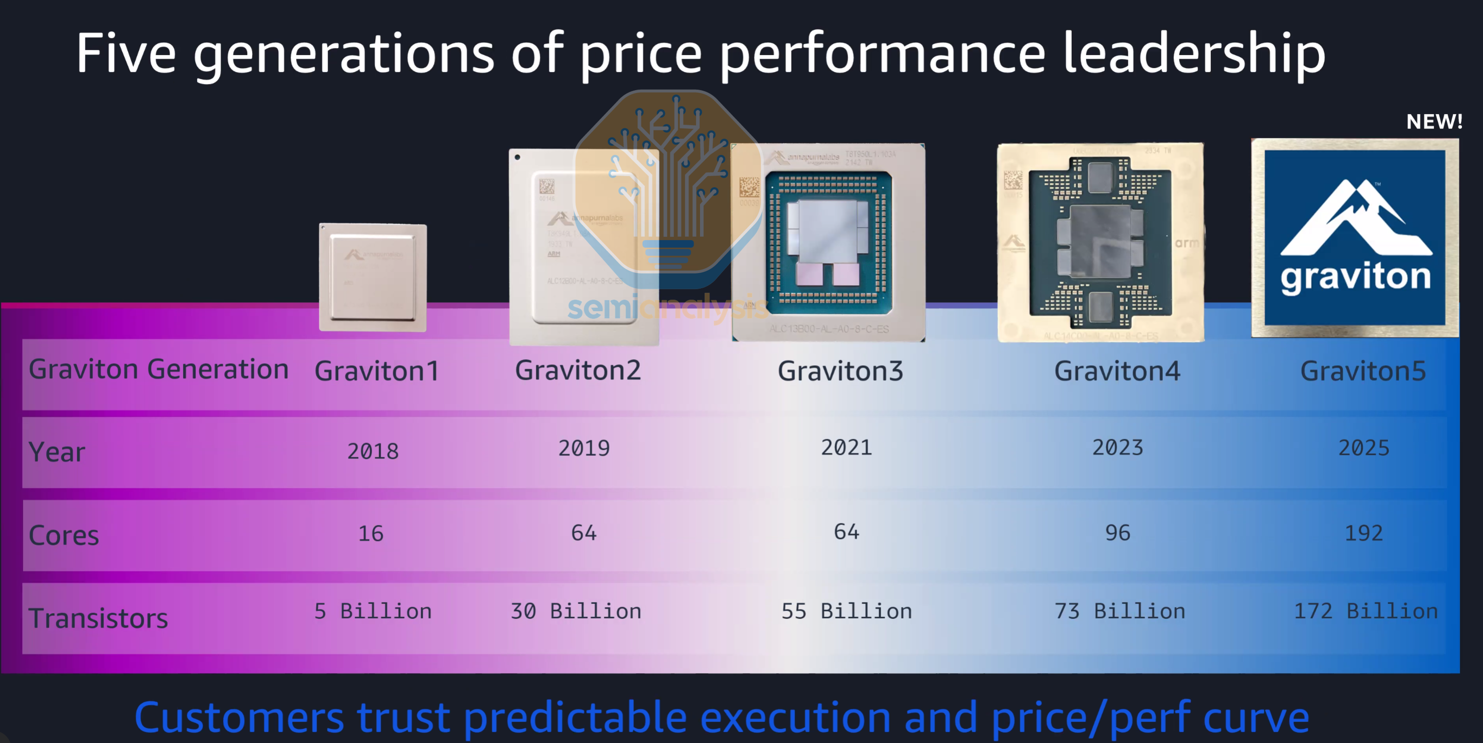
Amazon Web Services (AWS) was the first hyperscaler to successfully develop and deploy their own CPUs for the cloud. Thanks to the acquisition of the Annapurna Labs chip design team and ARM’s Neoverse Compute Subsystem (CSS) reference designs, AWS could now offer their EC2 cloud instances at lower prices thanks to a better margin profile by going directly to TSMC and OSAT partners for chip production as opposed to buying Intel Xeons.
The Graviton push started in earnest during the COVID boom with the Graviton2 generation, when AWS offered heavy discounting to entice cloud customers to port their programs over to the ARM ecosystem from x86. While not as performant on a per core basis compared to Intel’s Cascade Lake generation, Graviton2 brought 64 Neoverse N1 cores at a fraction of the price with significantly higher performance per dollar.
Graviton3’s preview in late 2021 brought several changes that focused on elevating per core performance to competitive levels. AWS moved to ARM’s Neoverse V1, a much larger CPU core with twice the floating point performance as N1, while keeping core counts at 64. A 10x7 Core Mesh Network (CMN) was employed with 65 cores printed on die, leaving room for 1 core to be disabled for binning. AWS also disaggregated the design into chiplets, with four DDR5 memory and two PCIe5 I/O chiplets surrounding the central compute die on TSMC N5, all connected with Intel’s EMIB advanced packaging. With the delays to Intel’s Sapphire Rapids, Graviton3 became one of the first datacenter CPUs to deploy DDR5 and PCIe5, a full year ahead of AMD and Intel, which we wrote about here.

Graviton4 continued scaling, adopting the updated Neoverse V2 core and increasing core counts and memory channels by 50% to 96 and 12-channels respectively, bringing 30-45% speedups over the previous generation. PCIe5 lane counts tripled from 32 to 96 lanes for much greater connectivity to networking and storage. Graviton4 also brought support for dual-socket configurations for even higher instance core counts.
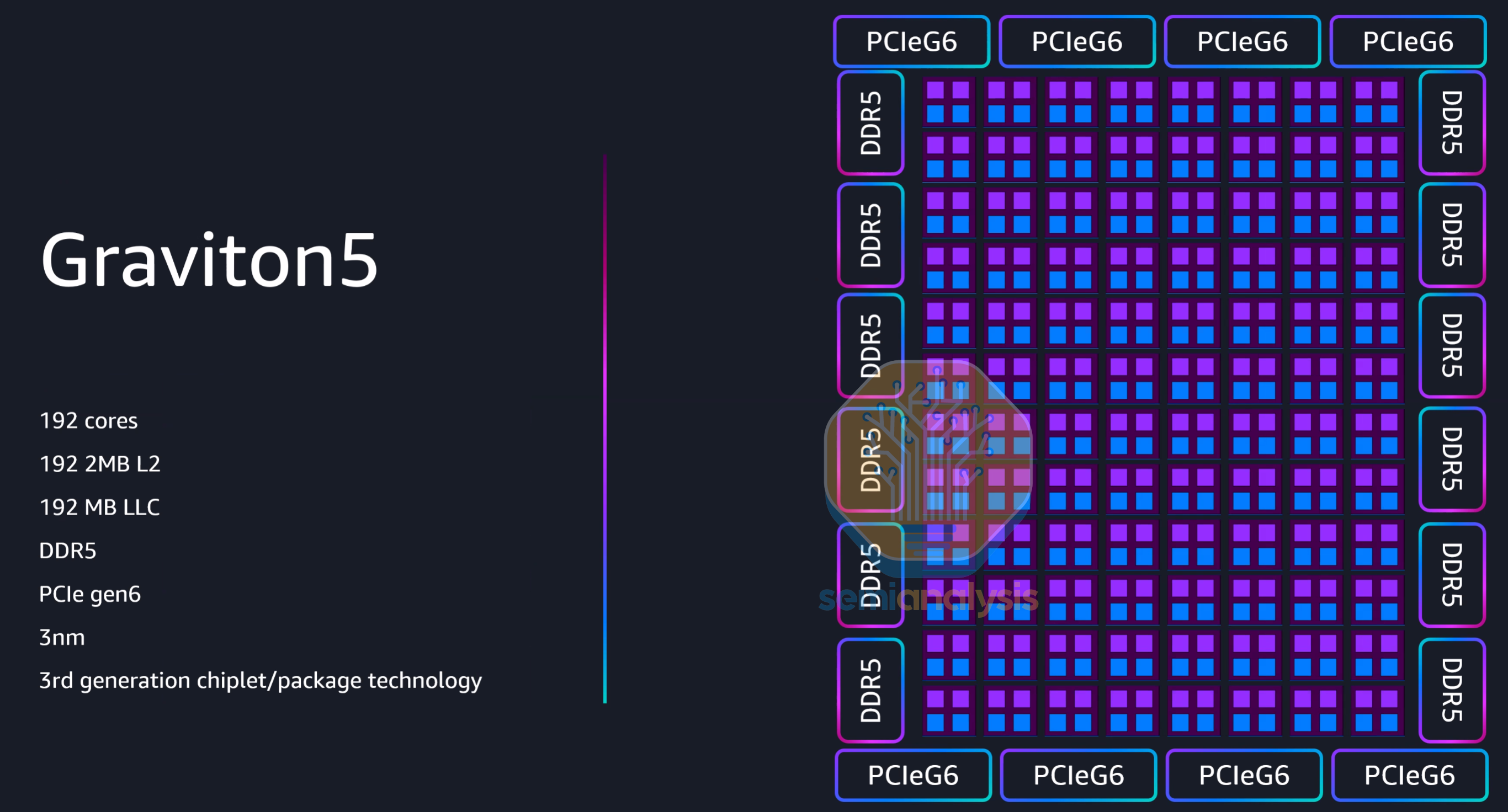
In preview since December 2025, Graviton5 features another huge jump in performance with 192 Neoverse V3 cores, double that of the previous generation, with 172 Billion transistors on TSMC’s 3nm process. While L2 cache per core remains at 2MB, the shared L3 cache increases from a paltry 36MB on Graviton4 to a more respectable 192MB on Graviton5, with the extra cache acting as a buffer as memory bandwidth only went up by 57% (12-channel DDR5-8800) despite doubling core counts.
The packaging of Graviton 5 is very unique as we discussed on Core Research and has large implications of a few vendors in the supply chain.
Interestingly, while the PCIe lanes were upgraded to Gen6, lane counts regressed from 96 lanes on Graviton4 to 64 on Graviton5, as apparently AWS was generally not deploying configurations using all PCIe lanes. This cost optimization saves Amazon alot on TCO while not impacting performance.
Graviton5 employs an evolved chiplet architecture and interconnect, with 2 cores now sharing the same mesh stop, arranged in an 8x12 mesh. While AWS did not show the packaging and die configurations this time, they ensured that Graviton5 does employ a novel packaging strategy, and that the CPU core mesh is split over multiple compute dies.
In terms of CPU usage, AWS was proud to mention that they have been using thousands of Graviton CPUs internally in their CI/CD design integration flows and to run EDA tools to design and verify future Graviton, Trainium and Nitro silicon, creating an internal dogfooding cycle where Gravitons design Gravitons. AWS also announced that their Trainium3 accelerators will now use Graviton CPUs as head nodes, with 1 CPU to 4 XPUs. While the initial versions run with Graviton4, future Trainium3 clusters will be powered by Graviton5.
Microsoft Cobalt 200
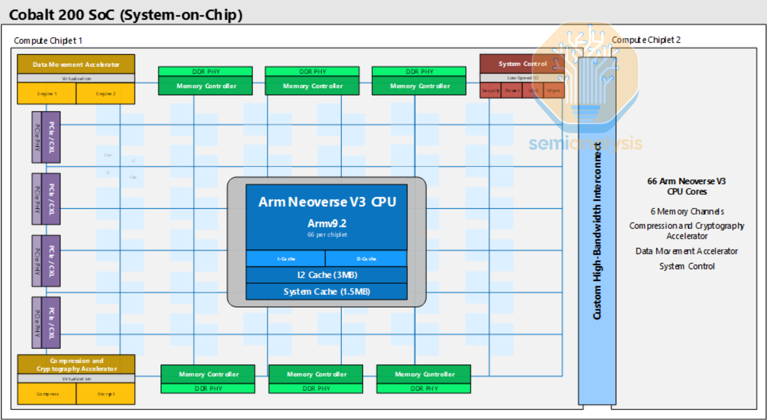

Following on from Microsoft’s first Cobalt 100 CPU in 2023 which we covered above, Cobalt 200 was launched in late 2025 with several upgrades. While core count did not increase much, going from 128 to 132, each core is now much more powerful with the Neoverse V3 design compared to the Neoverse N2 in the prior generation. Each core has a very large 3MB L2 cache, and are connected with the standard ARM Neoverse CMN S3 mesh network across two TSMC 3nm compute dies with a custom high-bandwidth interconnect between dies. From the diagram, each die has an 8x8 mesh with 6 DDR5 channels and 64 lanes of PCIe6 lanes with CXL support. 2 cores share each mesh stop, totaling 72 cores printed on each die with 66 enabled for yield. 192MB of shared L3 cache is also spread across the mesh. With these upgrades, Cobalt 200 achieves a 50% speedup over Cobalt 100.
Unlike Graviton5, Cobalt 200 will only be featured in Azure’s general purpose CPU compute services and will not be used as AI head nodes. Microsoft’s Maia 200 rackscale system deploys Intel’s Granite Rapids CPUs instead.
Google Axion C4A, N4A
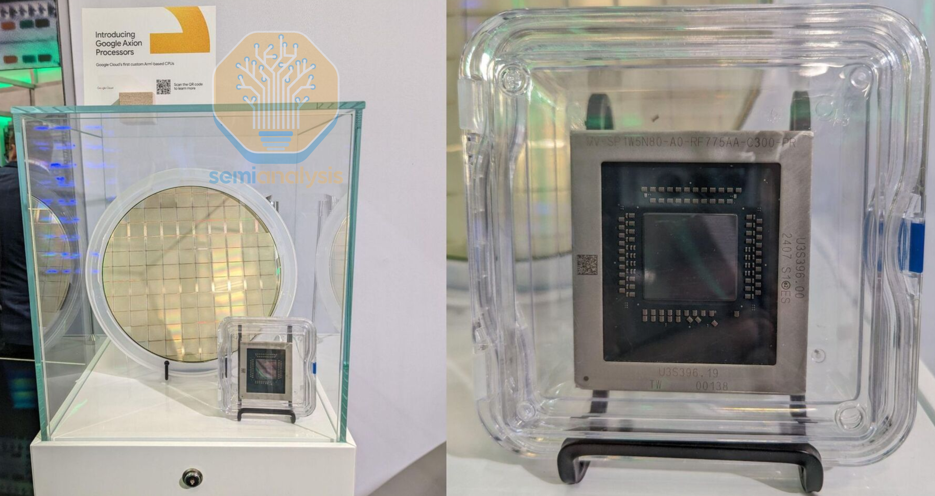
Announced in 2024 and generally available in 2025, The Axion line signaled Google’s entry into custom silicon CPUs for their GCP cloud services. Axion C4A instances have up to 72 Neoverse V2 cores on a standard mesh network, with 8 channels of DDR5 and PCIe5 connectivity on a large monolithic 5nm die. Based on close-up images of the Axion wafer presented at Google Cloud Next 2024, the die appears to have 81 cores printed in a 9x9 mesh, leaving room for 9 cores to be disabled for yield. Therefore, we believe a new 3nm die was designed for the 96-core C4A bare metal instances that went into preview late in 2025.
For more cost-effective scale-out web and microservices, Google’s Axion N4A instances are now in preview, coming with 64 lower performance Neoverse N3 cores on a much smaller die, allowing significant volume ramps through 2026. The Axion N4A silicon is a full custom design made by Google on TSMC’s 3nm process. As Google transitions their internal infrastructure over to ARM, Gmail, YouTube, Google Play and other services will run on Axion alongside x86. In the future, Google will design Axion CPUs for use as head nodes in their TPU clusters powering Gemini.
AmpereOne & SoftBank Acquisition
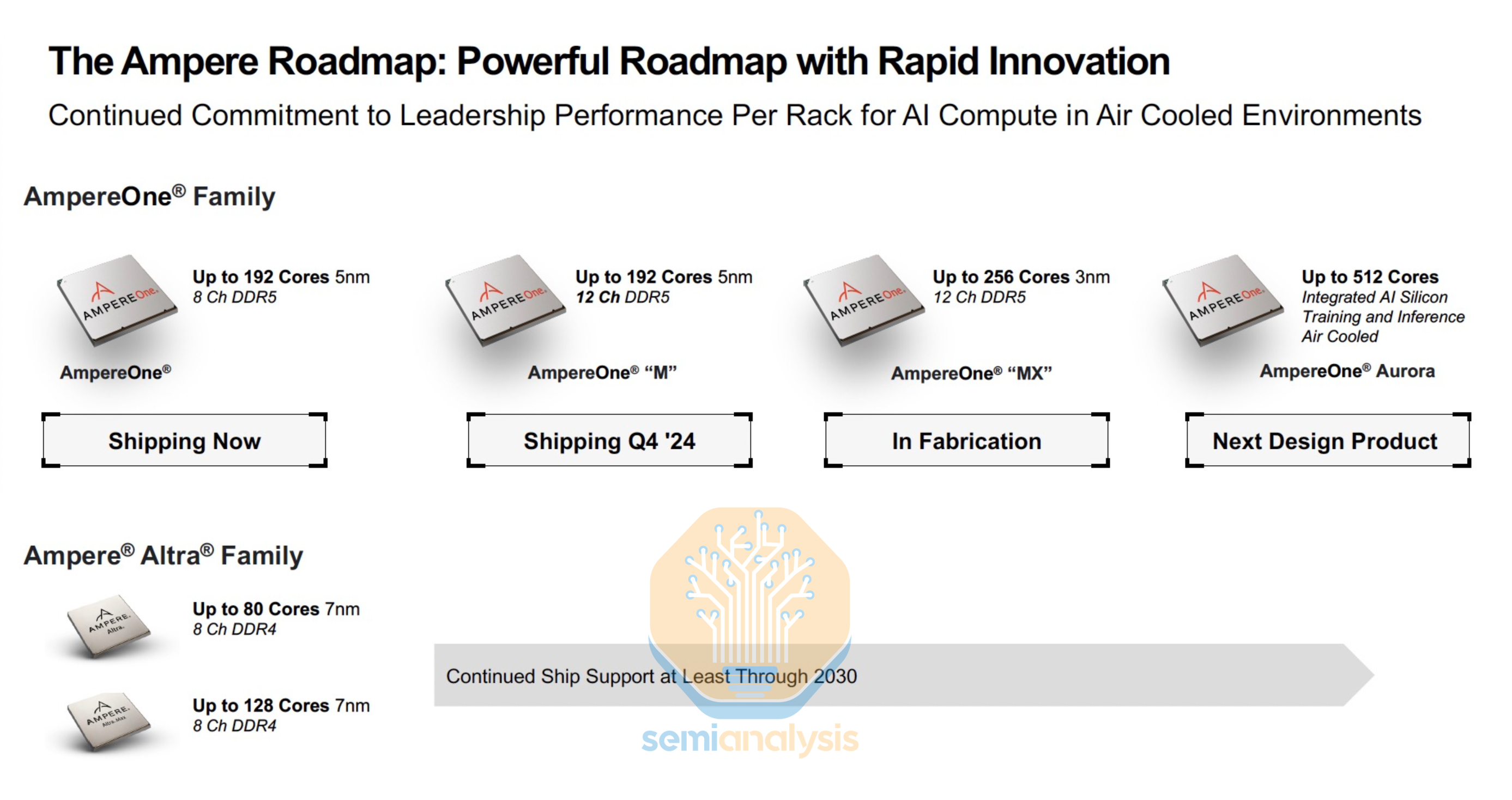
Ampere Computing was the original champion for merchant ARM silicon, competing directly with AMD and Intel as a 3rd silicon provider for OEM server builds. With a strong partnership with Oracle, Ampere delivered their 80-core Altra and 128-core Altra Max line of CPUs with great fanfare, promising to disrupt the x86 CPU duopoly with cost effective ARM CPUs. Ampere Altra employed the Neoverse N1 core with their own mesh interconnect with cores grouped into 4-core clusters. Accompanying the cores are 8-channels of DDR4 and 128 PCIe4 lanes on a single TSMC 7nm die.
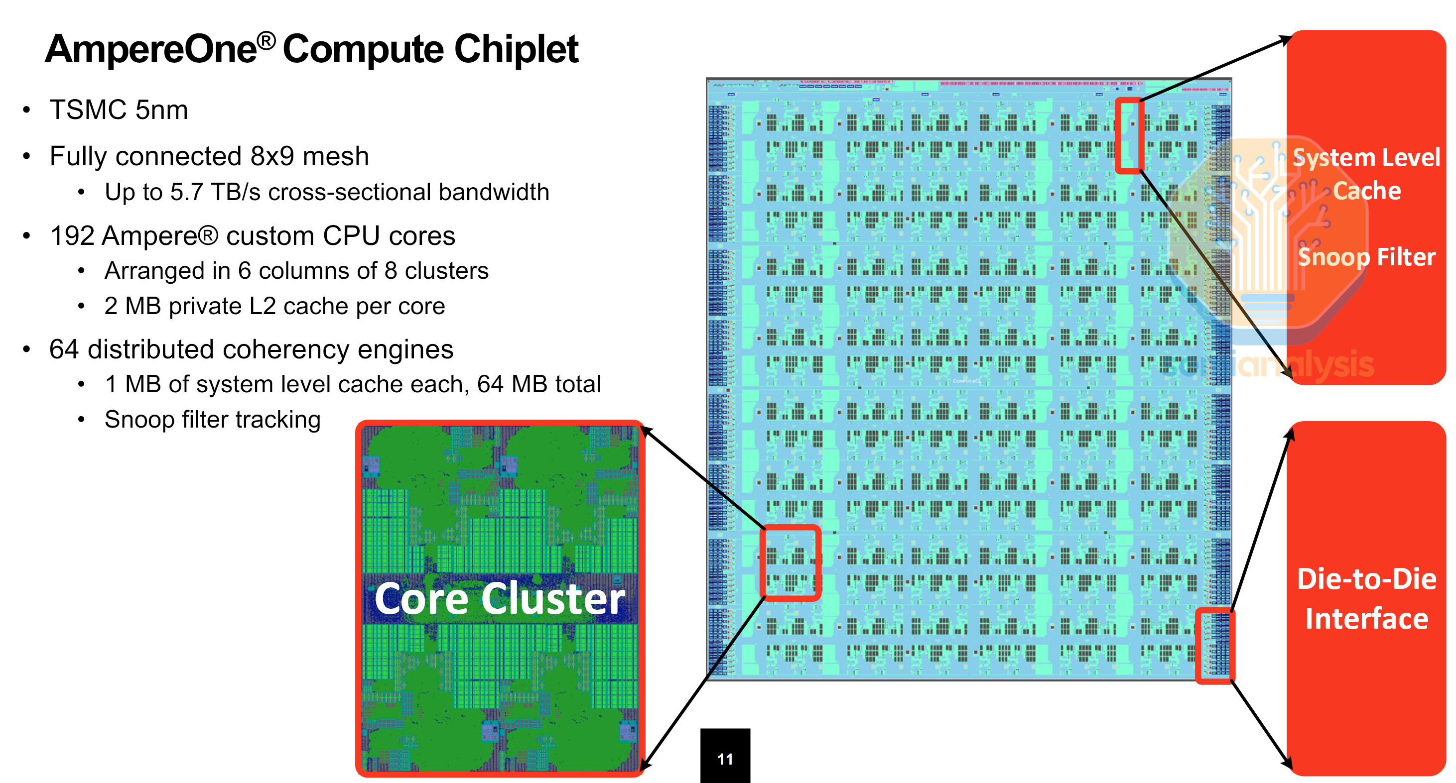
The next generation AmpereOne CPUs brought core counts up to 192, thanks to a move to a 5nm process and a novel chiplet design that disaggregates the IO into separate DDR5 and PCIe dies in an MCM configuration that does not require use of an interposer. Ampere also moved to a custom ARM core, designed for core density rather than outright performance, paired with an oversized 2MB L2 cache to minimize performance penalties from noisy neighbors where other VMs running on adjacent cores hog traffic on the shared mesh interconnect. A similar 4-core cluster is implemented on a 9x8 mesh network. In total, integer performance was doubled over Altra Max.
The chiplet design allows the same compute die to be reused in other variants, with the 12-channel AmpereOne-M adding 2 more memory controller dies. The future AmpereOne-MX reuses the same I/O chiplets but swaps in a 3nm compute die with 256 cores. Their 2024 roadmap also detailed a future AmpereOne Aurora chip with 512 cores and AI Training and Inference capabilities.
However, this roadmap is no longer valid once Ampere Computing was acquired by SoftBank in 2025 for $6.5 Billion. While true that Masayoshi Son wanted Ampere’s CPU design talent to shore up their CPU designs for the Stargate venture, the acquisition was also spurred by Oracle wanting to divest itself from a poorly performing business. Ampere’s CPUs never ramped into significantly high enough volumes due to timing and execution issues.
The Altra generation was their first major market entry, but arrived too early for mass adoption as most software was not ARM-native at the time. Unlike hyperscalers who could quickly adapt their internal workloads for their own ARM silicon, the general purpose and enterprise CPU markets are much slower to move. Following that, the AmpereOne generation faced many delays, with Oracle Cloud A2 and CPU availability arriving in the second half of 2024. By then, the hyperscaler ARM CPU projects are in full swing, and AMD could match Ampere’s 192 cores but with 3-4 times higher per core performance. Despite Oracle promoting Ampere instances with halved per-core licensing costs, the CPUs were not popular enough, and the order book dried up. Oracle never used up their full pre-payment for Ampere CPUs, with their Ampere CPU purchases dwindling from $48M in fiscal 2023 to $3M in 2024 and $3.7M in 2025.
Ampere is now working on AI chips as well as CPUs under the Softbank umbrella.
ARM Phoenix
ARM’s core IP licensing business has been very successful in the datacenter market, with nearly every hyperscaler adopting their Neoverse CSS designs for their custom CPUs. To date, over 1 Billion Neoverse cores have been deployed across datacenter CPUs and DPUs, with 21 CSS licenses signed across 12 companies. With increasing core counts and hyperscale ARM CPU ramps, datacenter royalty revenue more than doubled Year-over-Year, and they are projecting CSS to represent over 50% of royalty revenue in the next couple of years. Read our article here to learn more about ARM’s business model and how CSS extracts more value.

However, ARM is taking things further in 2026 and will be offering full datacenter CPU designs, with Meta as its first customer. This CPU, codenamed Phoenix, changes the business model by becoming a chip vendor, designing the entire chip from cores to packaging. This means that ARM will now compete directly with its customers who license the Neoverse CSS architecture. ARM, who are majority owned by SoftBank, are also designing custom CPUs for OpenAI as part of the Stargate OpenAI Softbank venture. Cloudflare is also looking to be a customer for Phoenix. We have detailed COGS, margin, and revenue in Core Research.
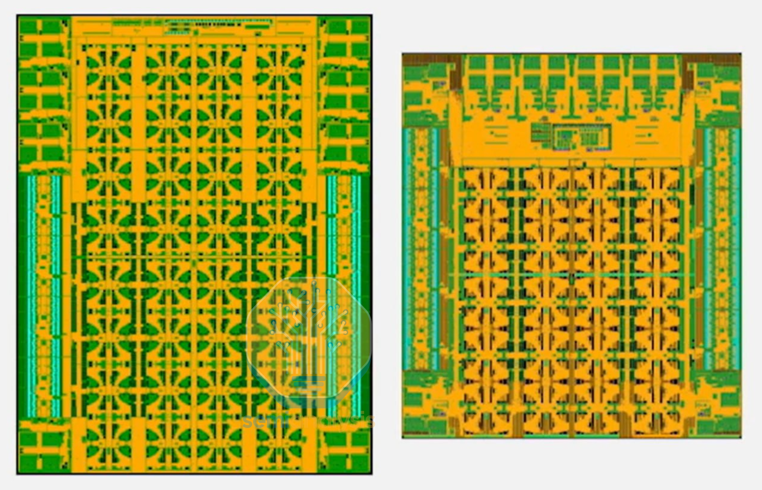
Phoenix has a standard Neoverse CSS design and layout that is similar to Microsoft’s Cobalt 200. 128 Neoverse V3 cores are connected with ARM’s CMN mesh network across two half-reticle size dies made on TSMC’s 3nm process. On the memory and I/O front, Phoenix features 12 channels of DDR5 at 8400 MT/s and 96 lanes of PCIe Gen 6. Power efficiency is competitive, with a configurable CPU TDP of 250W to 350W.
With this, Meta now has their own ARM CPU to match the likes of Microsoft, Google and AWS. As an AI head node, Phoenix enables coherent shared memory to attached XPUs over PCIe6 via an Accelerator Enablement Kit. We will detail the next generation ARM “Venom” CPU design for our subscribers below, including a significant memory change.
Huawei Kunpeng
China’s home grown CPU efforts are continuing apace, with both Loongson and Alibaba’s Yitian line offering locally designed options. However, the biggest player in the market is Huawei, who have refocused their datacenter CPU roadmap with their Kunpeng processor series. Huawei has some of the most capable design engineers from their HiSilicon team, with custom TaiShan CPU cores and data fabrics that are worth keeping an eye on.
Huawei’s first few generations of datacenter CPUs used the standard mobile ARM Cortex cores. The 2015 Hi1610 featured 16 A57 cores. 2016’s Hi1612 doubled core counts to 32, while the Kunpeng 916 in 2017 updated the core architecture to Cortex-A72. All three generations were fabbed on TSMC 16nm.
The Kunpeng 920 arrived in 2019 with an ambitious multi-chiplet design and 64 custom cores. Two compute dies on TSMC 7nm each contained 8 clusters of 4 TaiShan V110 cores running on the ARM v8.2 ISA. The clusters are connected with a ring bus to four channels of DDR4 on the same die totaling 8-channels across the two compute dies. Kunpeng 920 was the first CPU to adopt TSMC’s CoWoS-S advanced packaging, with a large silicon interposer connecting 2 compute dies to an I/O die with 40 PCIe Gen 4 lanes and dual integrated 100 Gigabit Ethernet controllers using a custom die to die interface. While Kunpeng 920 integrated many novel technologies, the US sanction on Huawei which curtailed their supply of TSMC had disrupted their CPU roadmap, as the next Kunpeng 930 generation failed to release in 2021.
Instead, an updated Kunpeng 920B was quietly released in 2024 with several upgrades. The TaiShan V120 cores now support SMT, with 10 clusters of 4 on each of the two compute dies for 80 cores and 160 threads. Core interconnect and layout remained similar to the Kunpeng 920 with 8 channels of DDR5 on the compute dies. The I/O die is now split into halves with the compute dies in the middle. We believe the 5 year gap between CPU generations were the result of US sanctions and having to redesign the chip for the SMIC N+2 process.
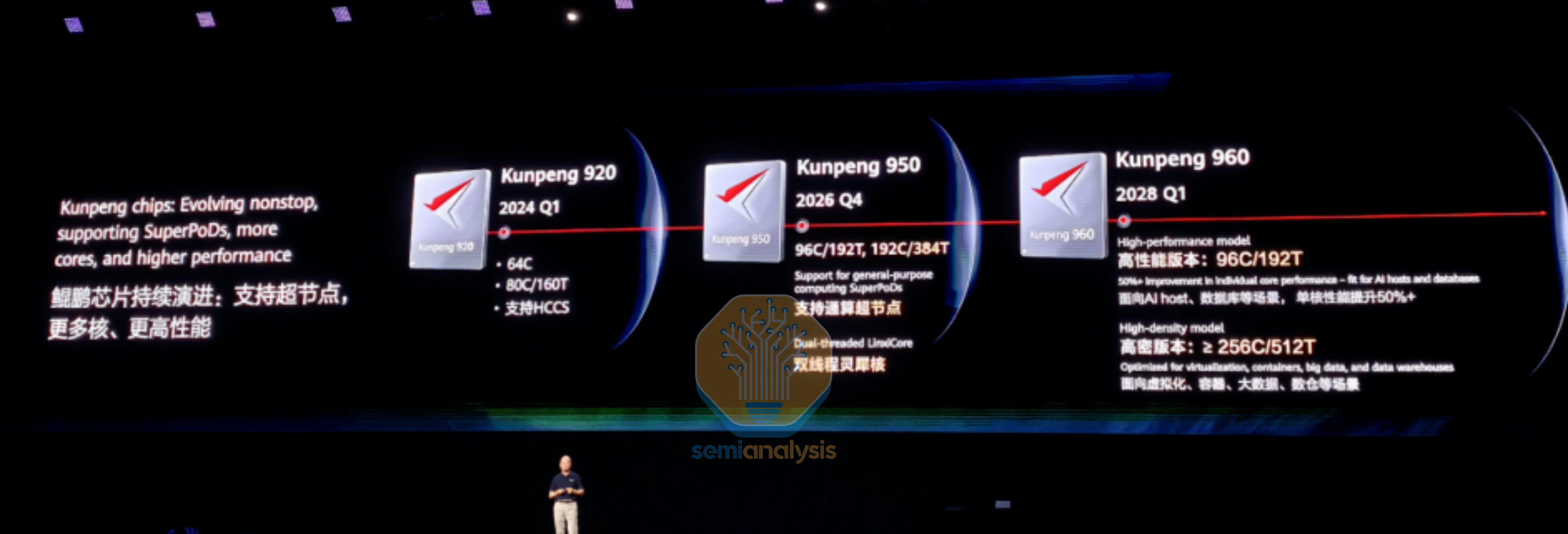
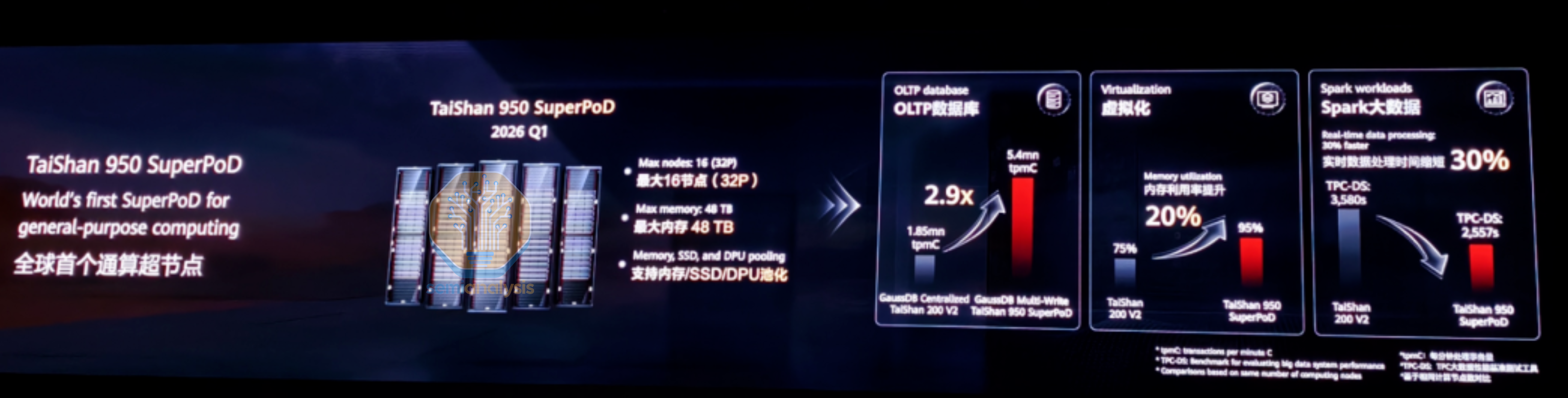
For 2026, Huawei is updating its CPU line again with the Kunpeng 950 and configuring them in TaiShan 950 SuperPoD racks for general purpose compute. Kunpeng 950 promises a 2.9x speedup on OLTP database performance over the Kunpeng 920B using their proprietary GaussDB Multi-Write distributed database architecture. To achieve this, core counts more than doubled to 192 using a new LinxiCore that retains SMT support. A smaller 96 core version will also be produced. 16 dual-socket servers go into each TaiShan 950 SuperPoD rack with up to 48TB of DDR5 memory, indicating a 12-channel memory design. These racks also integrate storage and networking, and will be adopted by Oracle’s Exadata database servers and used by China’s finance sector. The design will likely be produced on SMIC’s N+3 process that recently debuted in the Kirin 9030 smartphone chip.
Huawei’s roadmap continues into 2028 with the Kunpeng 960 series. This generation follows the trend of splitting the design into two variants. A 96 core, 192 thread high performance version will be made for AI head nodes and databases that promises a 50%+ improvement in per core performance, while a high-density model for virtualization and cloud compute will increase core counts to 256 and possibly beyond. By then, we expect Huawei to take significant share in Chinese hyperscaler CPU deployments.
Below we present our CPU roadmap to 2028, and detail the key features and architectural changes of the datacenter CPUs beyond 2026, including AMD’s Verano and Florence, Intel’s Coral Rapids and cancelled CPU lines, ARM’s Venom specifications, Qualcomm’s return to the datacenter CPU market with SD2, and include NVIDIA’s Bluefield-4 as a sign of how CPU deployments are evolving going forward. We then discuss the impacts of the DRAM shortage on each datacenter CPU segment and look at future CPU trends, highlighting crucial design aspects that will shape CPUs in the next decade.