Is SMIC N+3’s Metal Pitch Smaller than Intel 18A’s?
SMIC N+3 Node Deep Dive vs TSMC N6, TechInsights Private Equity Sale, SemiAnalysis Teardown Engineering & Evaluation Lab, HiSilicon Kirin 9030, Process Technology, Patterning, Cell Architecture
Almost four years ago, we published that SMIC had started shipping 7 nm (N+1) chips. Now, SMIC is shipping its third-generation 7 nm (N+3) process in Huawei’s Kirin 9030, with a minimum metal pitch of 32.5 nm, about 10% tighter than the 36 nm minimum metal pitch shipping in Intel’s latest Panther Lake CPUs on 18A.
The headline is true, but an incomplete cherry picked metric. N+3 reaches the density of TSMC N6 through aggressive DUV multi-patterning and design-technology co-optimization (DTCO), but it pays for that in complexity, efficiency and process control.
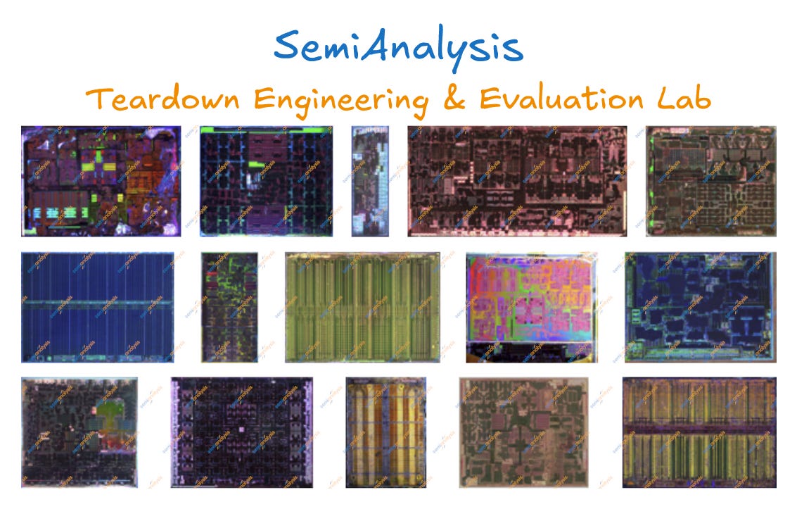
We found this and more in our reverse engineering and teardown where we cover SMIC’s N+3 process technology, Huawei’s packaging, memory, architecture, and other exciting features. SemiAnalysis has been building a state-of-the-art teardown lab in Oregon capable of analyzing the world’s most advanced and important chips over the last year and a half. We have already generated revenue on advanced datacenter chip teardowns including our recent reverse engineering of a major TSMC customer’s COUPE CPO optical engine + EIC 3D stack.
This is the first public report from the SemiAnalysis Teardown Engineering & Evaluation Lab, or STEEL for short. The lab is aggressively scaling up and out and we’re excited to announce it publicly. This is a bit of inconvenient timing for TechInsights as they are private equity owned and currently being sold while having enjoyed virtually no credible competition for decades. This has led to TechInsights underinvesting in CAPEX.
SemiAnalysis exceeds TechInsights in revenue despite no venture or private equity ownership and being founded only 6 years ago. Because we have no external investors and are founder-led, we move faster, build faster, and we can release client chip teardowns for free regularly, while focusing on datacenter for our major clients.
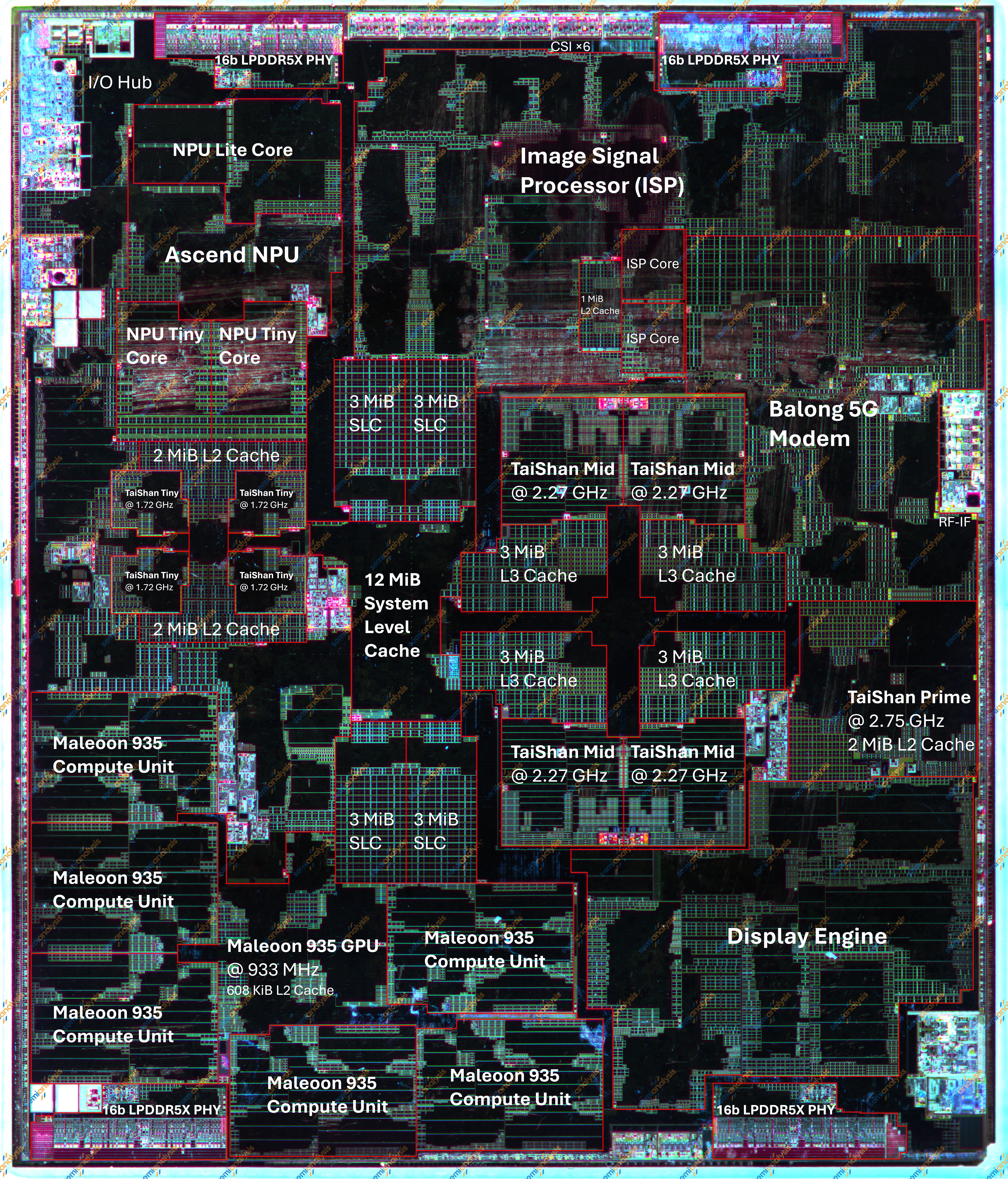
Here’s the first public image from our lab, the HiSilicon Kirin 9030 Pro SoC:
This report will detail our teardown of the Kirin 9030 and our findings on SMIC’s N+3 process, the most advanced in China. For comparison, we’ll show our teardown of the MediaTek Helio G99, made on TSMC N6. Through this comparison, we can look at the effect of export controls – SMIC N+3 and TSMC N6 are comparable nodes, but one is heavily export-controlled, the other free to use the West’s most advanced equipment.
Here we see both China’s progress and constraints. SMIC N+3 reaches TSMC N6-class logic density, but it requires far more aggressive DUV multi-patterning, so it does not match N6 on process maturity or cost. The Kirin 9030 Pro performs similarly to three-year-old Android flagships, and trails far behind the current flagship SoCs from Apple, Qualcomm, MediaTek, and Samsung. The efficiency gap is even wider.
Export controls have not stopped Huawei and SMIC from shipping advanced silicon, but they have forced a different path. Without EUV, SMIC is leaning harder on DUV multi-patterning, DTCO, and increasingly complex integration. The roadmap continues forward through tighter design rules and backside power, but each step adds cost and process risk. Huawei’s τ scaling and LogicFolding show another path: stacking active logic and recovering density through advanced packaging and system-technology co-optimization (STCO).
Die Shot & Floorplan
To understand the Kirin 9030, we must first understand Huawei’s SoC history. HiSilicon is Huawei’s chip design arm, responsible for the Kirin smartphone SoCs, Kunpeng server CPUs, Ascend AI accelerators, and switch/router networking silicon.
Before export controls, Huawei was one of TSMC’s largest customers – the only customer on TSMC’s first EUV node, N7+, and among the first on N5, alongside Apple. That ended in late 2020. Huawei switched to Qualcomm SoCs in its flagship smartphones, though export controls limited them to 4G-only variants.
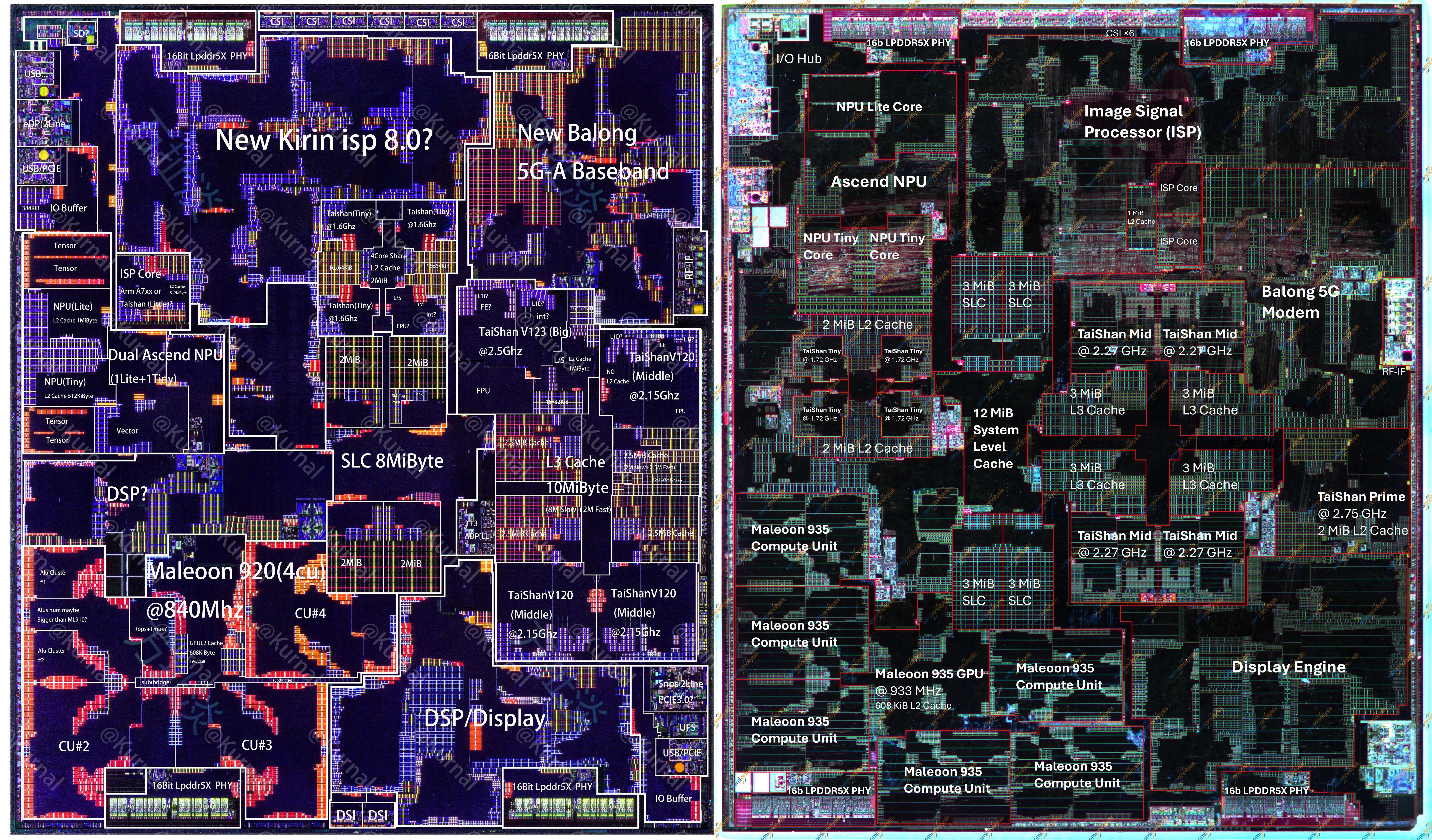
In late 2023, Huawei returned to in-house silicon with the Kirin 9000s, a successor to the Kirin 9000, fabricated on SMIC N+2 instead of TSMC N5. In the following years, they released the Kirin 9010 and 9020 on the same N+2 process. These chips used Huawei’s in-house TaiShan CPU cores and Maleoon GPU.
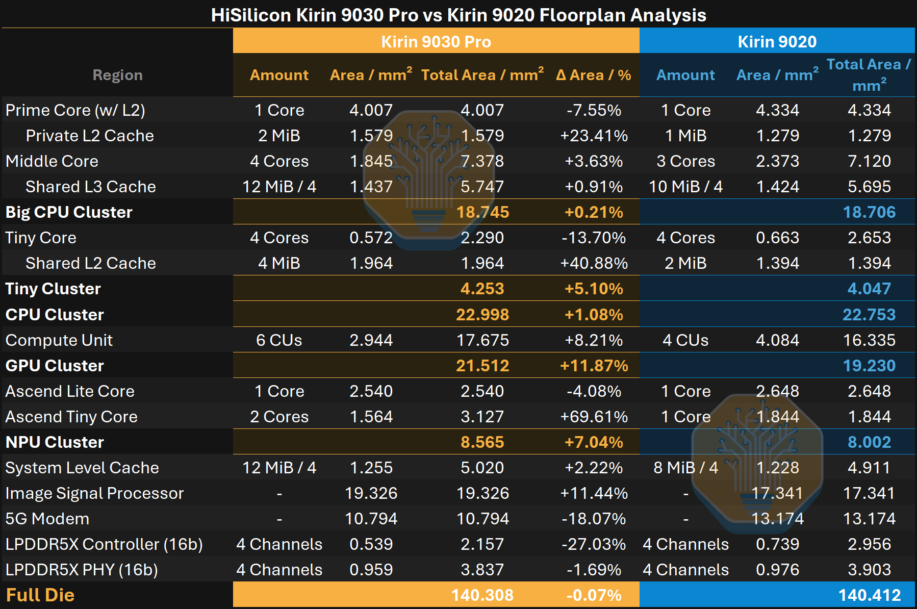
We have not torn down a Kirin 9020 ourselves, so the predecessor die shot is from Kurnal. The die shots show how Huawei spent its silicon budget: which functional blocks are where, and how their areas compare to the predecessor.
First, a quick guide to the major blocks on the die.
The total die area is nearly identical, but the 9030 uses that area more aggressively. A denser process lets Huawei fit an extra middle CPU core, more GPU and NPU cores, and larger caches into the same footprint.
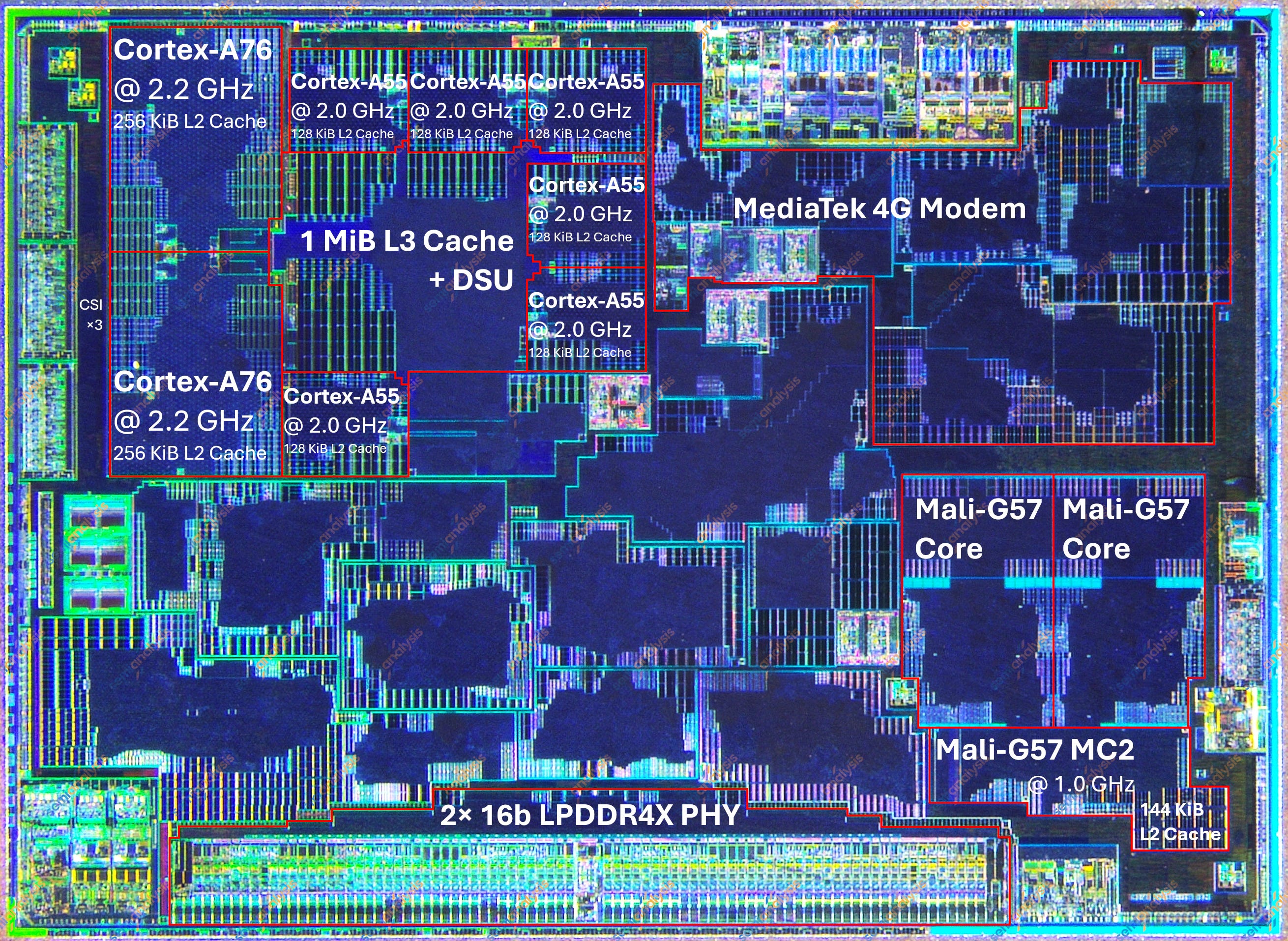
In contrast, the Helio G99 is a much smaller, low-cost SoC, built for budget smartphones rather than a flagship device. While the Kirin 9030 is ~140 mm², the G99 is only ~29 mm², roughly one-fifth the area. The underlying TSMC process technology, however, is directly comparable as a baseline for analyzing SMIC’s.
Architecture & PPA
The Kirin 9030 is an evolutionary refresh, not a clean-sheet design. Its CPU, GPU and NPU cores carry over the 9020’s families, and the gains come from three levers: the SMIC N+2-to-N+3 process step, DTCO and floorplan work, and incremental microarchitecture. Area is where the first two show up, and the 9030 scales well here. Performance and efficiency are the harder test. Huawei’s design holds up better than its node would suggest, but the chip still trails, both because N+3 sits behind the leading-edge nodes and because its cores, while competent, remain a few generations behind the newest designs.
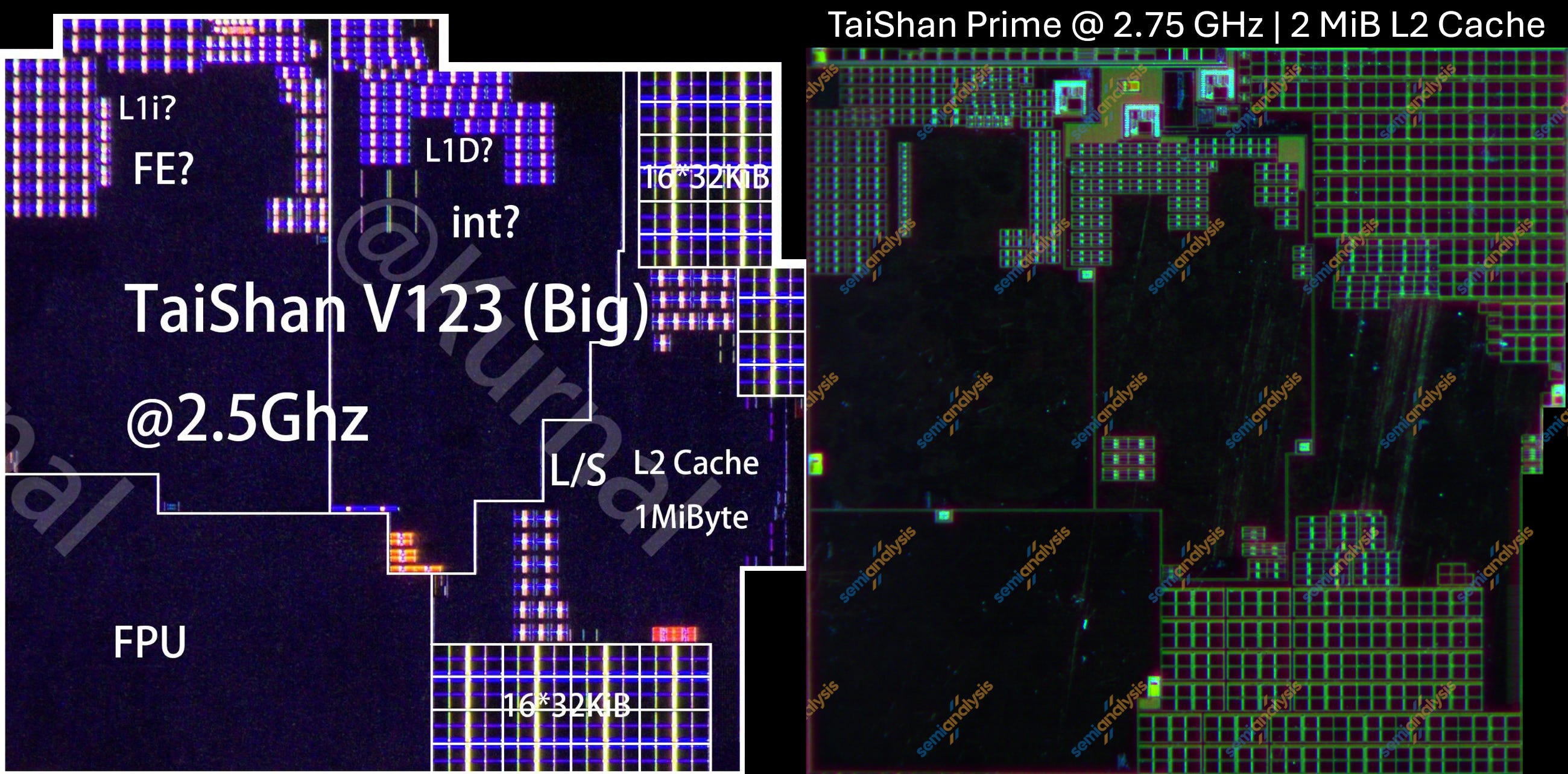
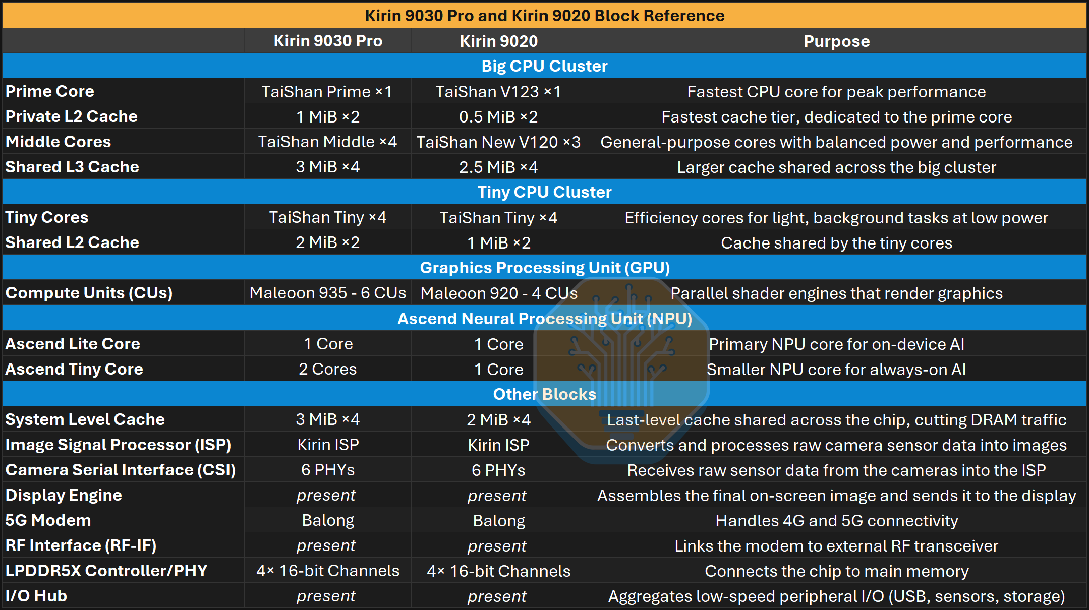
The new prime core is an incremental update. The main changes are a 10% frequency increase from 2.5 GHz to 2.75 GHz and a doubling in the L2 cache from 1 MiB to 2 MiB. Despite the increased cache, the core size decreased by 7.6%. Excluding the private L2 cache, the core size decreased by 21%. This is a large reduction for an incremental node.
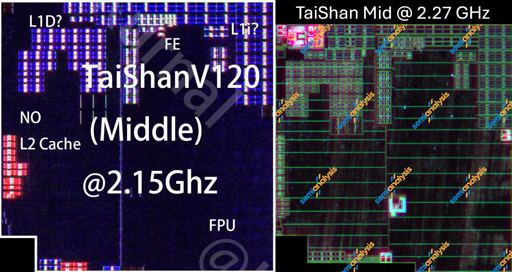
Compared with the TaiShan New V120 core in the Kirin 9020, the Kirin 9030’s middle core is almost unchanged architecturally, yet each core shrinks by ~22%. Most of that comes from the move from N+2 to N+3, with layout likely accounting for the rest.
Visually, the most noticeable change is the increase from 3 middle cores to 4. There is also a 20% increase in the shared L3 cache of the big cluster. This helps to improve multi-core performance without sacrificing much in terms of area.
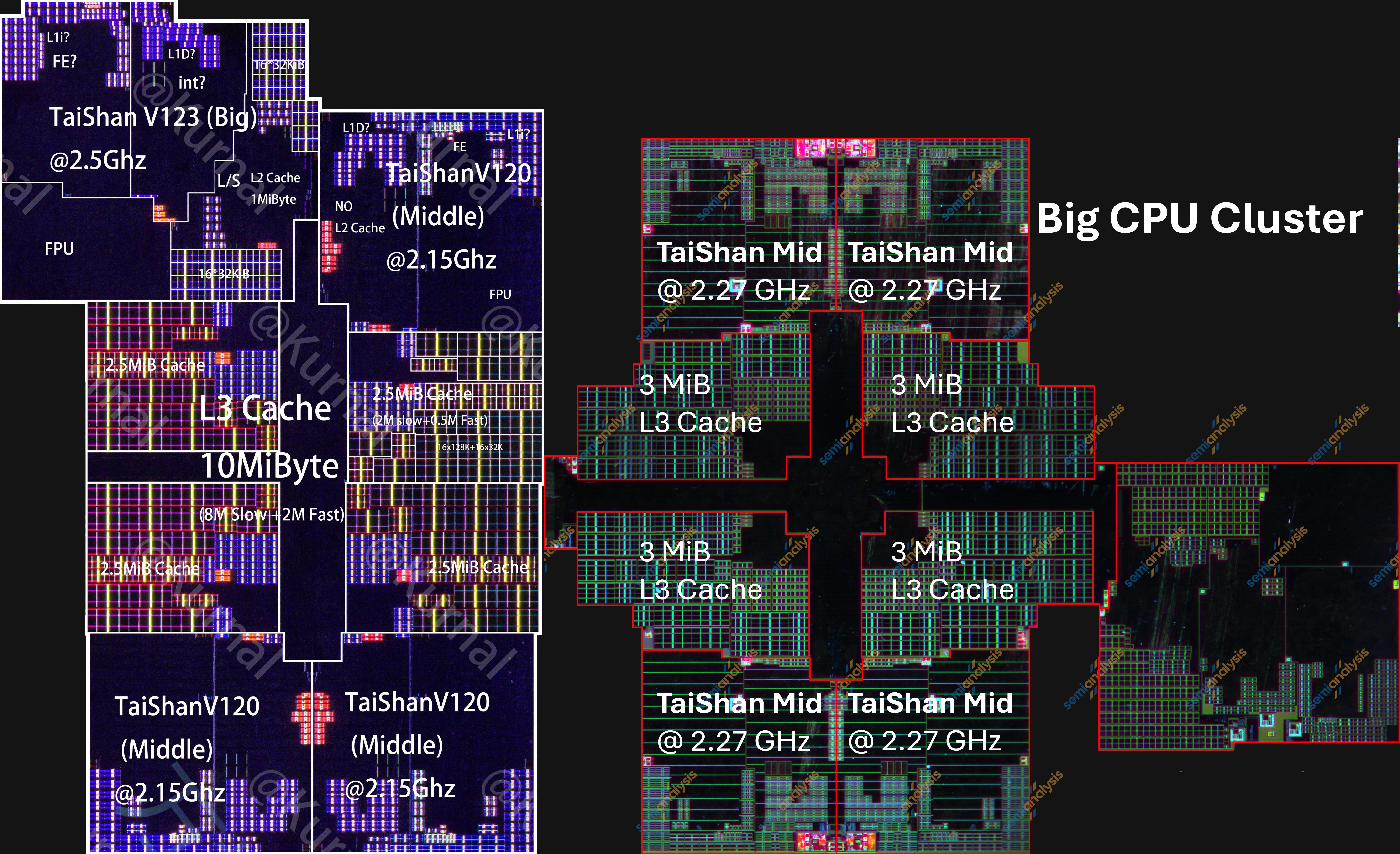
Even with each core shrinking, the big CPU cluster’s total area is essentially unchanged. The per-core savings went back into an additional middle core and larger caches.
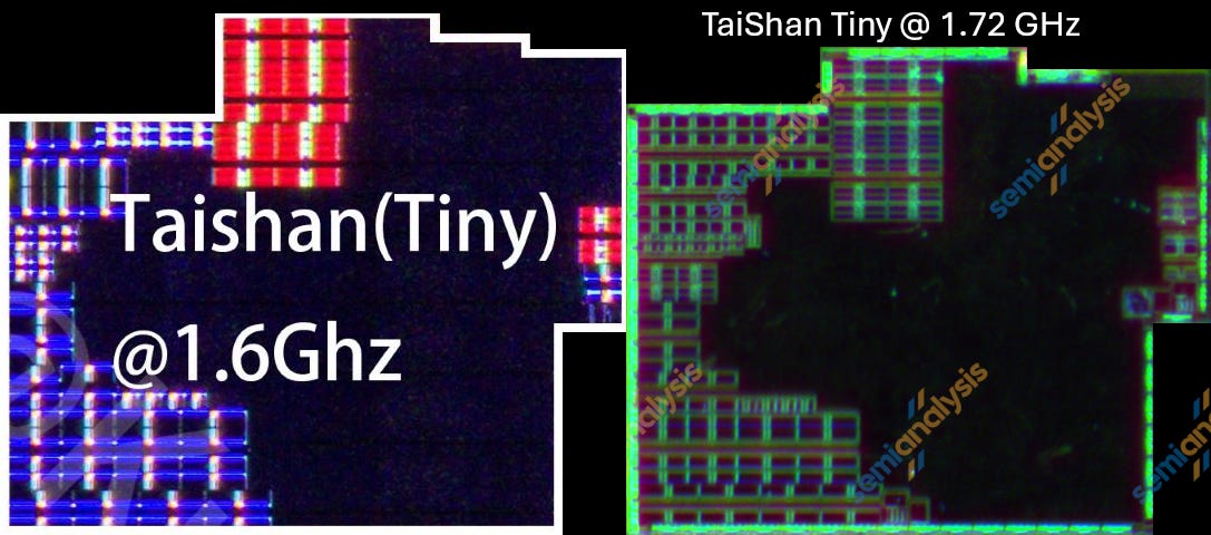
The tiny cores shrank less than the prime core (excluding its L2 cache) and less than the middle cores. This is likely because fixed overhead is a larger share on a small core. We cannot resolve any architectural changes from the die shot alone, but the per-clock and efficiency gains shown below point to more than pure process and layout scaling. The area reduction was offset by a doubling of the shared L2 cache from 2 MiB to 4 MiB, leaving the total tiny CPU cluster area slightly larger.
Area is the easiest improvement to see from a die shot, but it is only one part of PPA (power, performance, area). For modern logic, power and performance matter just as much, and often more. Since Dennard scaling broke down in the mid-2000s, voltage and frequency have not scaled in step with transistor dimensions, so each node has had to fight harder for gains in performance and efficiency.
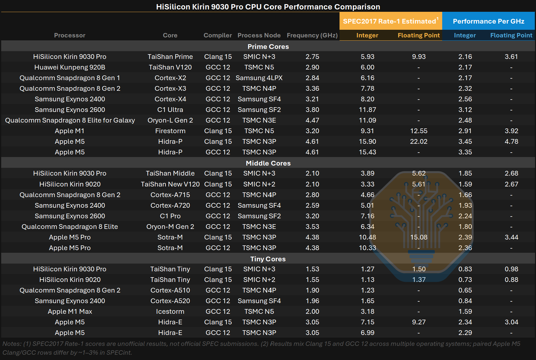
The starkest comparison is not Kirin 9020 versus Kirin 9030 Pro. Apple’s efficiency cores run circles around Huawei’s prime core. Apple’s low-power core delivers 20% higher integer performance while drawing only 1 W, compared with 4.5 W for Huawei’s prime core. N+3 matches TSMC N6, but N6 is several generations old. Apple and Qualcomm build on N4 and N3P, which are denser and sit on a better voltage-frequency curve, giving them a larger transistor budget and more performance per watt.
The 9030’s own cores did improve. The middle and tiny cores gained 17% and 14% in per-clock integer performance over the 9020, with floating-point flat on the middle core and up 11% on the tiny. The tiny core improves cleanly, with performance rising while power falls and efficiency increases by 45% in integer and 24% in floating point. The middle core is mixed: integer performance rises but power rises faster, cutting integer efficiency by 7%, while lower power lifts floating-point efficiency 16%.
Per-clock gains at the same or lower frequency are microarchitectural, so the cores are tuned, not just shrunk. Both also failed to hold their rated maximum frequencies, pointing to thermal, power, or stability limits. Per clock, the middle core sits around Arm Cortex-A720 and the tiny core near the Cortex-A520; absolute performance trails because Huawei clocks them much lower.
The prime core is roughly Cortex-X2 class per clock, a 2021 design. Apple’s 2020 M1 Firestorm core is still 35% higher per clock and 57% faster in absolute integer performance at a similar 4.5 W. The current leading edge is further ahead again: the Apple M5 P-core is 60% higher per clock and 2.7× faster, the Arm C1 Ultra 45% higher and 2× faster.
Matching older high-end cores per clock is a genuine design achievement. What Huawei cannot match is the voltage-frequency curve and transistor budget of leading-edge nodes, which let Apple, Qualcomm and others spend more transistors in the same area on wider cores, larger caches and deeper buffers while running at lower voltage.
Huawei’s LogicFolding roadmap is one answer, stacking active logic to recover density and shorten signal paths. We return to it later.
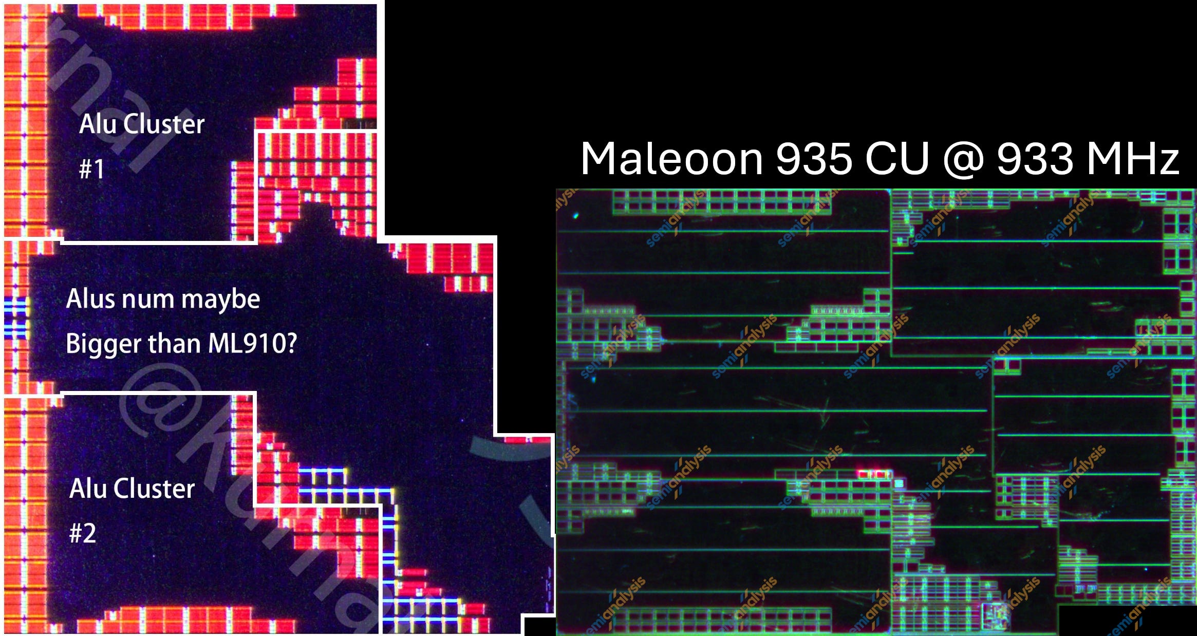
The GPU compute units (CUs) changed more visibly than the CPU cores, moving to a more rectangular layout for both the arithmetic logic unit (ALU) clusters and the CU overall. Even with ray-tracing support added, a CU shrank ~28%.
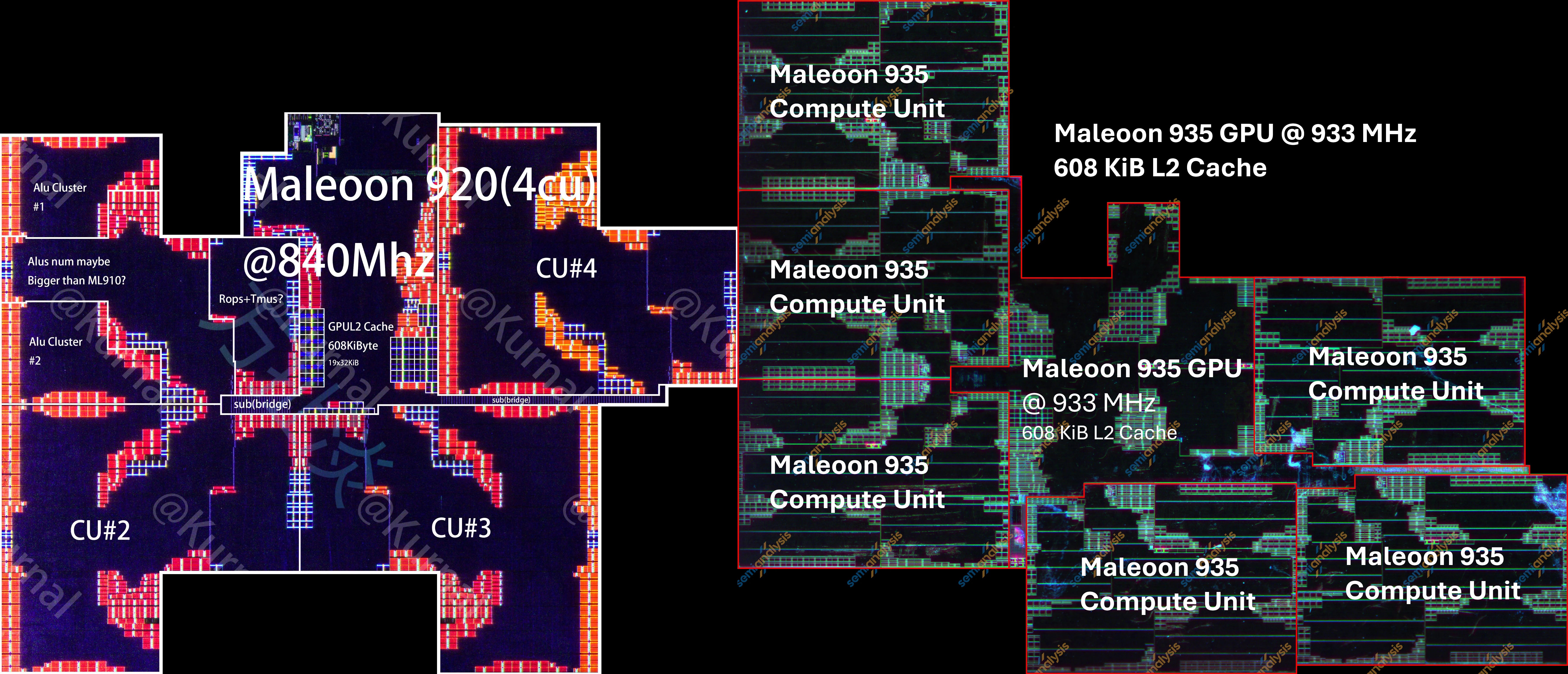
However, that shrink is offset by the increase from 4 to 6 CUs and the area outside the CUs grew 33%. Overall, the GPU cluster is larger by ~10%.
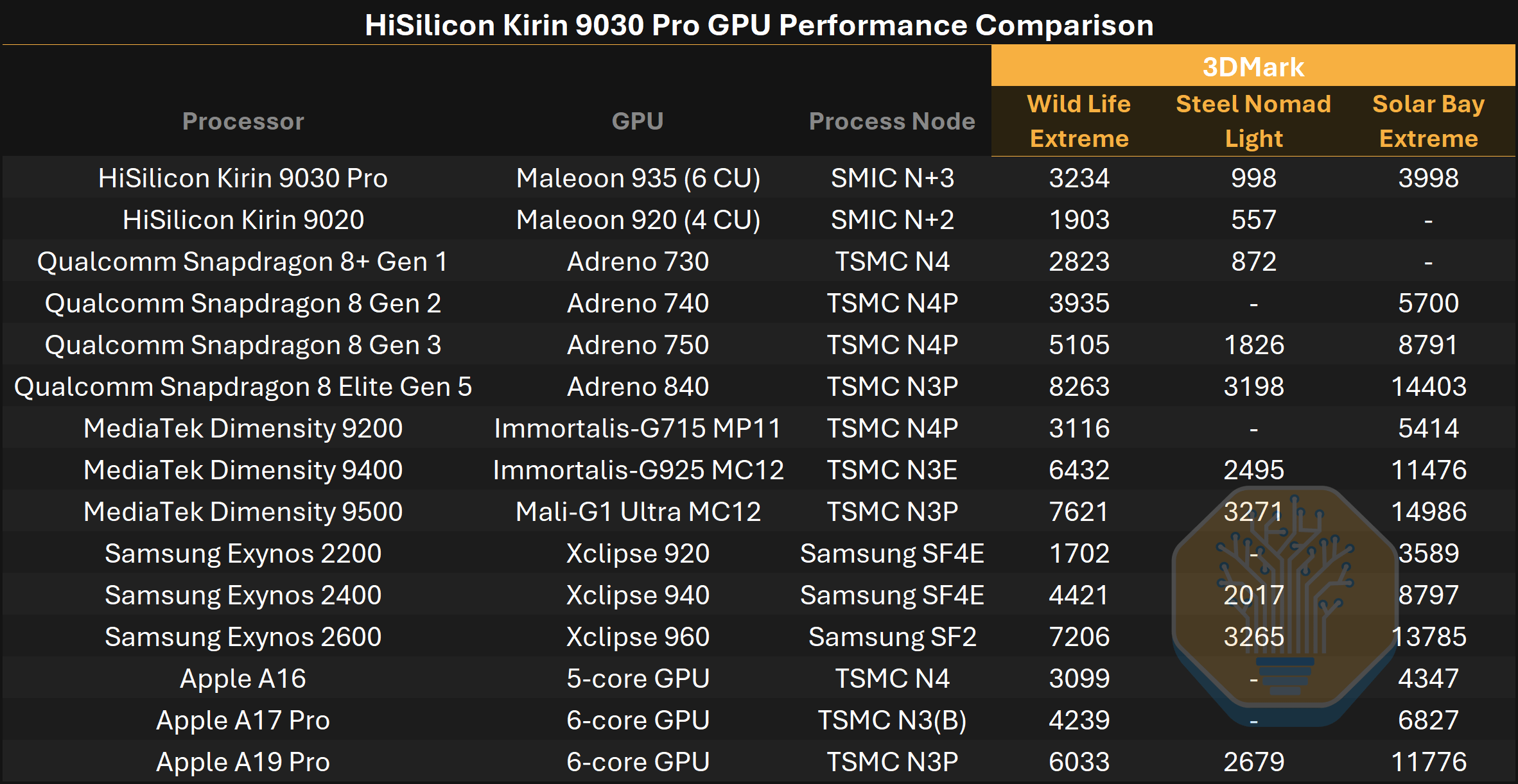
The GPU is where Huawei makes its biggest gains. The Maleoon 935 is not competitive with current flagships, but it is a large step up from the 920 and reaches older-flagship territory. In 3DMark it is 70% faster in Wild Life Extreme (WLE) and 79% faster in Steel Nomad Light (SNL) than the 920; with 11% higher clocks and 50% more CUs, the ~67% theoretical uplift roughly matches WLE and is beaten by SNL.
It edges ahead of the Snapdragon 8+ Gen 1 in WLE and SNL, and the Dimensity 9200 and Apple A16 in WLE, but stays far behind newer parts: the Snapdragon 8 Elite Gen 5 and Dimensity 9500 are ~2.4–2.6× faster in WLE and ~3.2× faster in SNL.
The Maleoon 935 is Huawei’s first GPU with hardware-accelerated ray tracing; there it lands slightly ahead of the Exynos 2200, and on par with the Apple A16, with current flagships up to 3.7× faster.
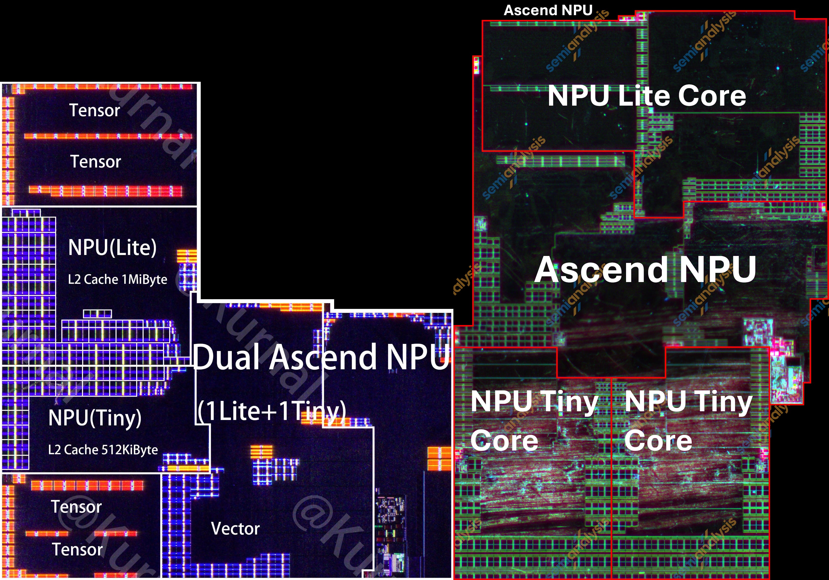
The Neural Processing Unit (NPU) saw the largest structural changes of any block, moving from a Lite and a Tiny core in the Kirin 9020 to a Lite and two Tiny cores in the Kirin 9030. Both core types also show significant layout changes.
This is a reversal in Huawei’s NPU design. The Kirin 9000 5G, its last flagship chip on TSMC N5, used two Lite and one Tiny core. The series of SoCs on SMIC N+2 moved to one Lite and one Tiny core, likely for area savings. With the Kirin 9030, Huawei has shifted back toward a larger multi-core NPU cluster, but with the additional area going to a Tiny core rather than a Lite core.
We’re diving deep into the most advanced datacenter and AI hardware hitting the market. To learn more about what’s in the pipeline or to commission a custom teardown, contact sales@semianalysis.com. Interested in joining us on this ride and think you can be a difference maker? Check out our Careers page.
Before diving into the process stack, the package and memory are worth separating from the SoC itself.
Memory
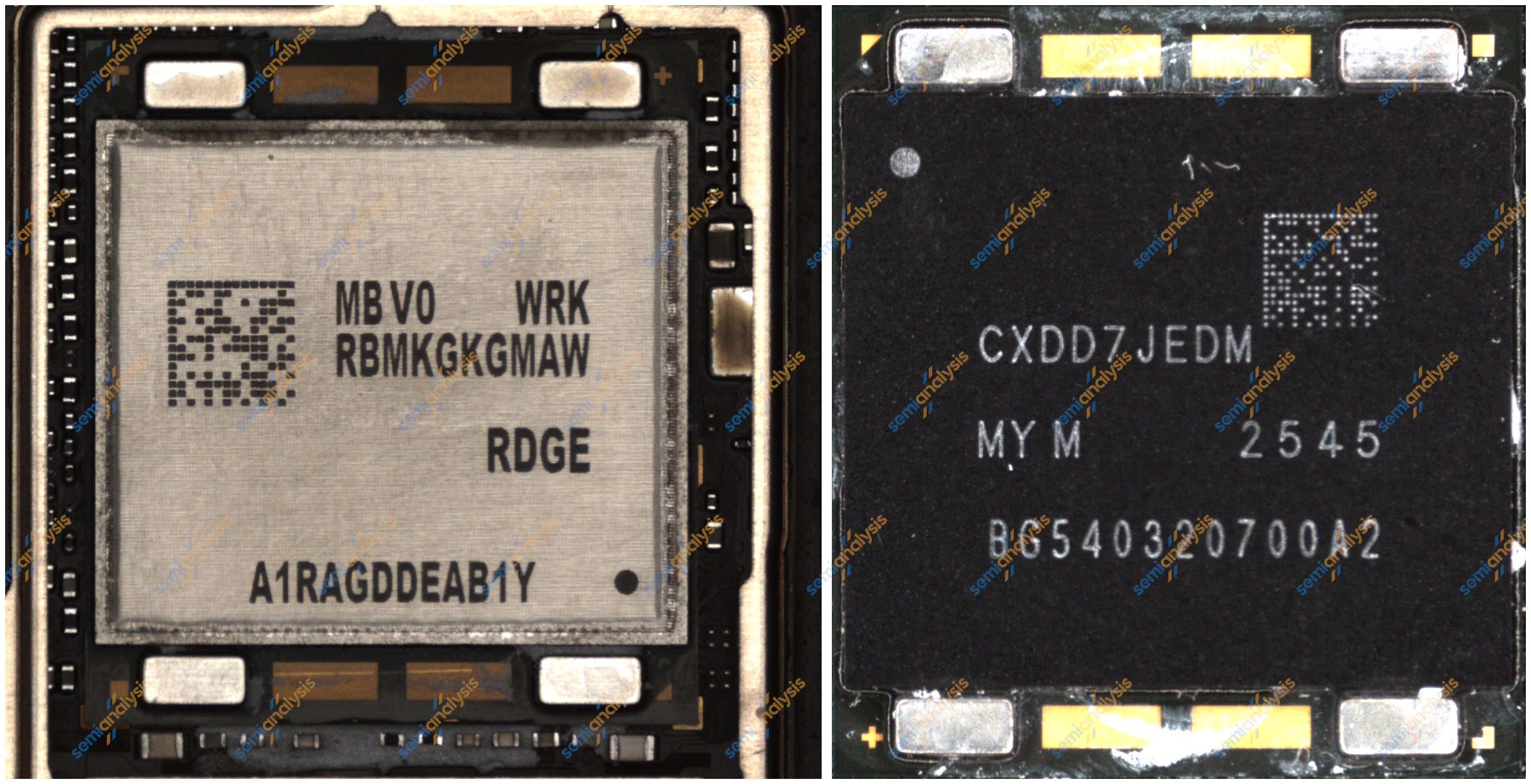
The Pro variant of the Kirin 9030 carries 12 GB of Samsung DRAM, with two stacks of four dies each. The dies were identified as the K4L2E165YD, a 12 Gb LPDDR5X-9600 device fabricated on Samsung’s 1a node, the fourth generation of its 10 nm-class DRAM after 1x, 1y and 1z. 1a has shipped in volume since 2022, so this is current memory rather than older-node inventory.
The 16 GB Pro Max variants we obtained were found with both CXMT and Samsung packages. The CXMT package is marked CXDD7JEDM, with two stacks of four dies, packaged in week 45 of 2025. The inferred die dimensions from X-ray computed tomography (CT) are consistent with a known density of ~0.3 Gib/mm² for the CXMT G4 process, roughly equivalent to other manufacturers’ 1z processes.
Packaging
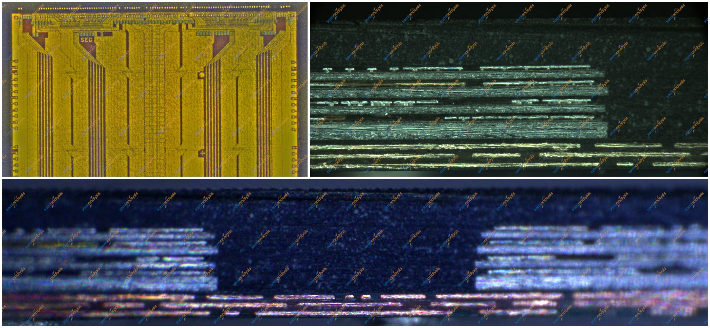
The Kirin 9030 uses a typical integrated package-on-package (iPoP) stack: multiple DRAM dies in a memory package sit above an organic redistribution layer (RDL) interposer, which sits above the SoC and package substrate. The full package is then mounted to the printed circuit board (PCB) through ball-grid array (BGA) solder bumps.
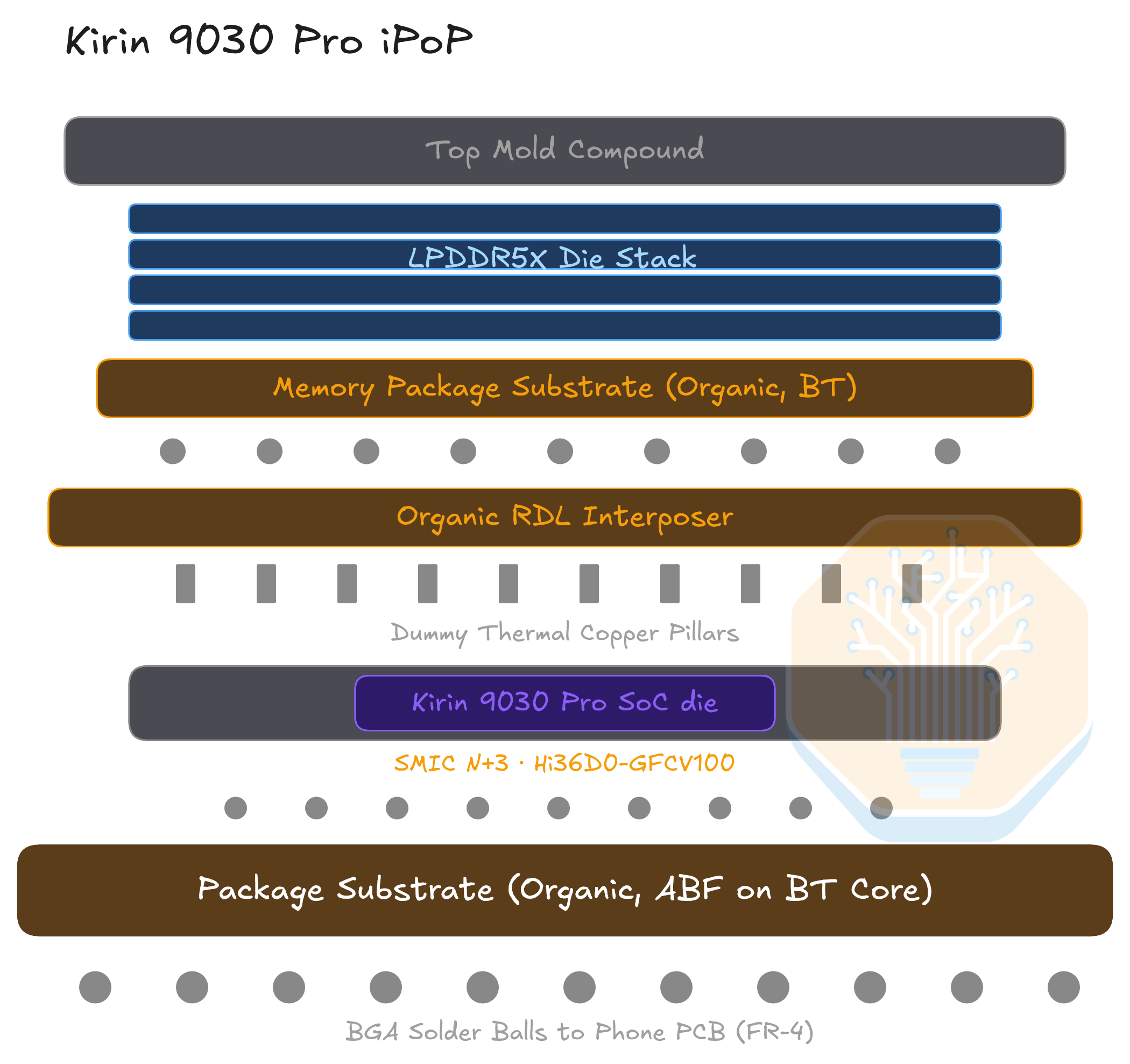
The memory package substrate is a thin bismaleimide-triazine (BT) laminate carrying the LPDDR5X stack. The organic RDL interposer over the SoC routes the PoP signals around the die and carries possible dummy thermal copper pillars. The package substrate, a thicker Ajinomoto Build-up Film (ABF) build-up over a BT core, fans the flip-chip bumps out to BGA pitch and embeds the power planes.
The whole stack is organic. The only silicon is the SoC and the LPDDR5X dies; there is no silicon interposer. Keeping it all-organic brings the package’s coefficient of thermal expansion (CTE) close to the PCB’s, reducing board-level warpage, and avoids the cost of a silicon interposer the SoC’s bandwidth does not need.
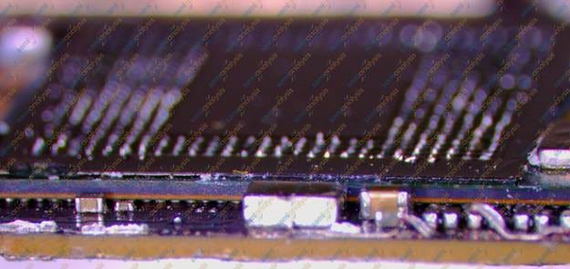
In an iPoP stack, the memory package connects to the organic RDL interposer through an array of solder bumps. Underfill fills the gap around those bumps, adding stiffness and protecting the joints from mechanical stress. The Pro and Pro Max variants differ here, which we cover behind the paywall.
Process
The die shot and architecture tell us how Huawei allocated its silicon budget. The process tells us what SMIC can manufacture. We use the Helio G99 as the process reference for TSMC N6. Both SMIC N+3 and TSMC N6 are evolutions of previous 7 nm-class nodes.
We used targeted TEM cross-sections through logic and memory regions, imaged in both fin-cut and gate-cut directions. Each cross-section caption gives its horizontal field width (HFW), the real width of the imaged area. We start at the transistor fins, then move up through standard cells, local interconnect, and SRAM.
SMIC has not overtaken Intel or TSMC. It uses aggressive DUV scaling and DTCO to reach N6-class density, but that density doesn’t translate into comparable performance and efficiency, for two reasons: the node gap to leading-edge nodes, and Huawei’s core designs.
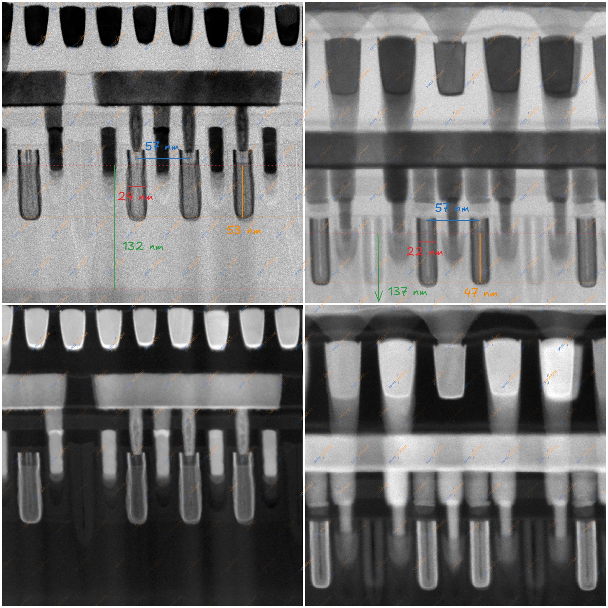
Fin Profile
One of the most important knobs in a FinFET process is the fin profile: the shape of an individual fin and the channel where current passes from source to drain. The ideal fin is tall, narrow, and nearly vertical. A taller fin increases effective channel width, while a narrower fin improves electrostatic control by thinning the body the gate must control. Push either too far, and the process pays for it: weaker drive current, fragile fins, taper, footing and line-edge variation that hit yield and device variability.
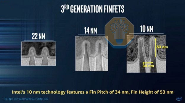
The Intel 22 nm, 14 nm, and 10 nm fin cross-sections show how FinFET nodes have improved over time. 22 nm fins were a first-generation structure, relatively short, wide and strongly tapered. The shape limits current density and reduces gate control uniformity across the height of the fin. At 14 nm and 10 nm, Intel pushed the fins taller and narrower while also making the sidewalls more vertical. Rather than shrinking the device, these changes increase the effective channel width per fin and improve electrostatic control. The trade-off is that taller fins at tighter pitches are much more difficult to manufacture.
Now, let’s compare the Helio G99 on TSMC N6 with the Kirin 9030 on SMIC N+3. Both processes are in the same class, with fin pitch of 30-32 nm on N+3 and 34 nm in our N6 cross-section. The pitch for N6 is especially interesting as N7’s HD library is generally listed with a 33 nm fin pitch, and N6 did not shrink pitches directly. Its density gains came from DTCO instead of tighter pitches. The 34 nm pitch was stable across our sampled region and serves more as a comparison against the SMIC N+3 we have not investigated further.
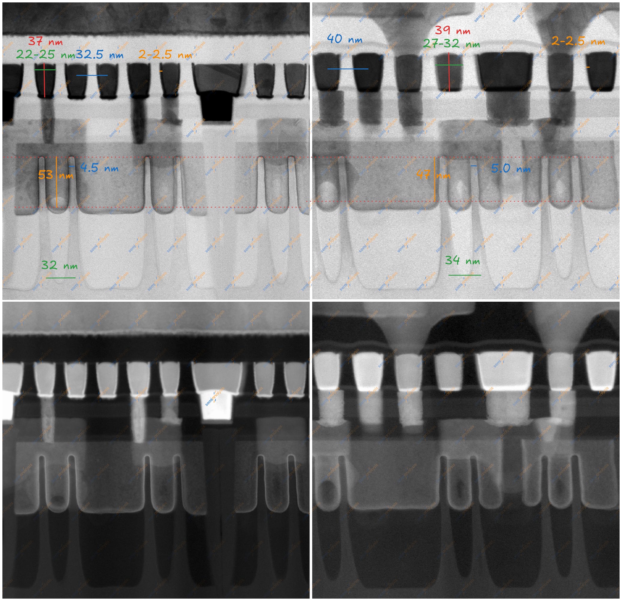
Pinning down N+3’s fin patterning scheme takes more than one core unit. The CPU cores show a dense ~32 nm pitch, with the pitch between N-P fin pairs alternating between 78 and 88 nm. Logic alone may be consistent with dual-pitch mandrels of 120 and 110 nm, but this is a complex and unusual approach. Combining the pitch from the the 8T SRAM, which has more complex repeat unit, with the CPU core sequence allows us to reverse engineer the patterning steps with more confidence.
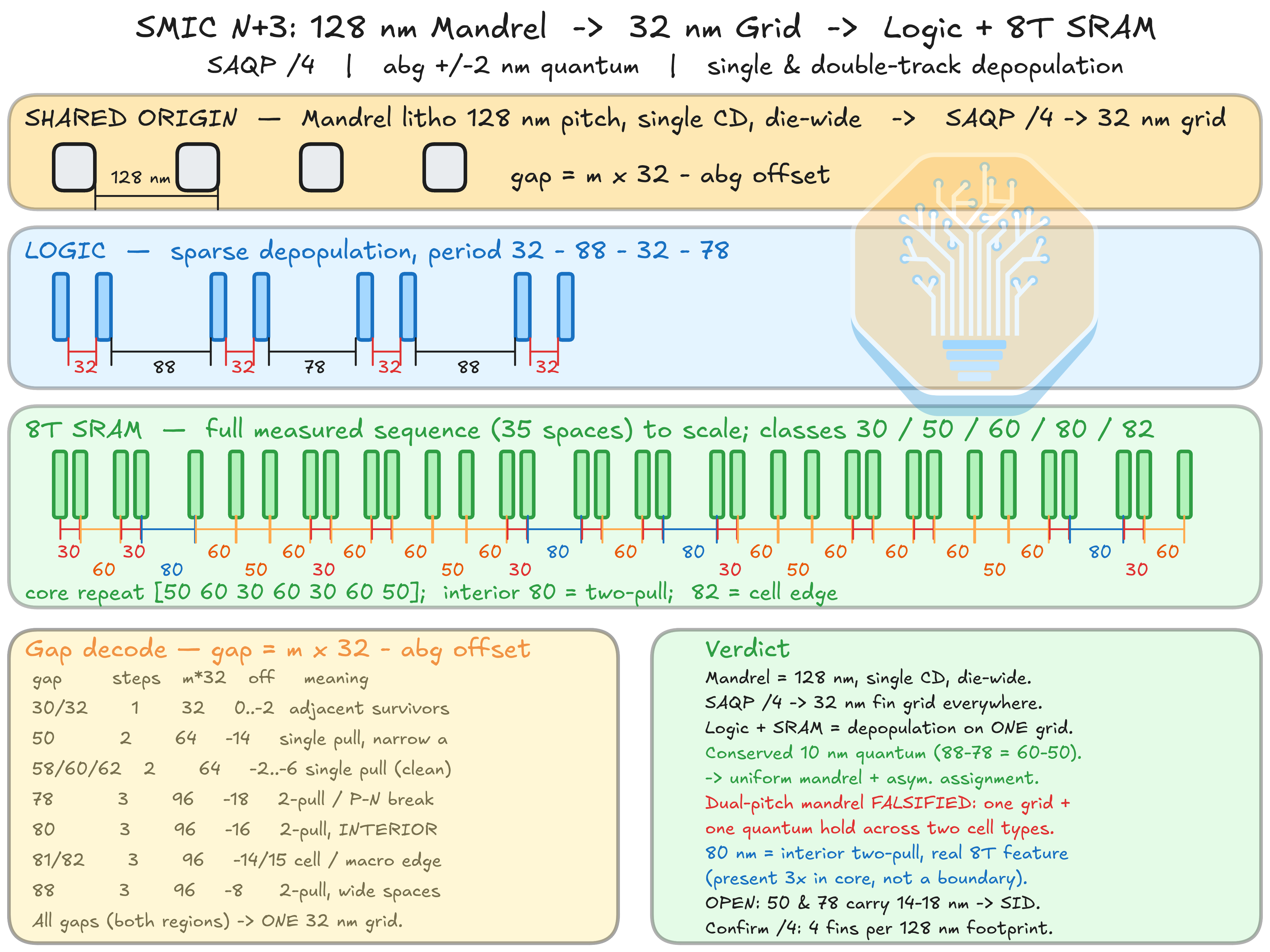
As both the logic and SRAM should share the same base grid, a single CD mandrel lithography pattern with 128 nm pitch undergoing SAQP produces a die-wide ~32 nm grid (128 nm/4), which supports the pitch sequencing seen in both logic and SRAM cells.
In the sampled cross-sections, N+3 shows a taller, narrower, higher-aspect-ratio fin than N6. The measured fin aspect ratio is ~9.5:1 on N+3 versus 7.8:1 on N6. N+3 also shows less top rounding, with an estimated radius of ~2 nm, compared with 2.8 nm on N6. Even though the fin widths differ, the ratio of top rounding to fin width tells the same story, with N+3 at 0.37 and N6 at 0.44. In a geometric sense, lower is better; a perfectly rectangular fin would have no top-rounding penalty.
These are single-digit-nanometer features measured from a handful of cuts, so treat the absolute numbers as approximate. The important result is the relative gap: N+3’s fins are consistently taller, narrower and less rounded than N6’s.
We’re diving deep into the most advanced datacenter and AI hardware hitting the market. To learn more about what’s in the pipeline or to commission a custom teardown, contact sales@semianalysis.com. Interested in joining us on this ride and think you can be a difference maker? Check out our Careers page.
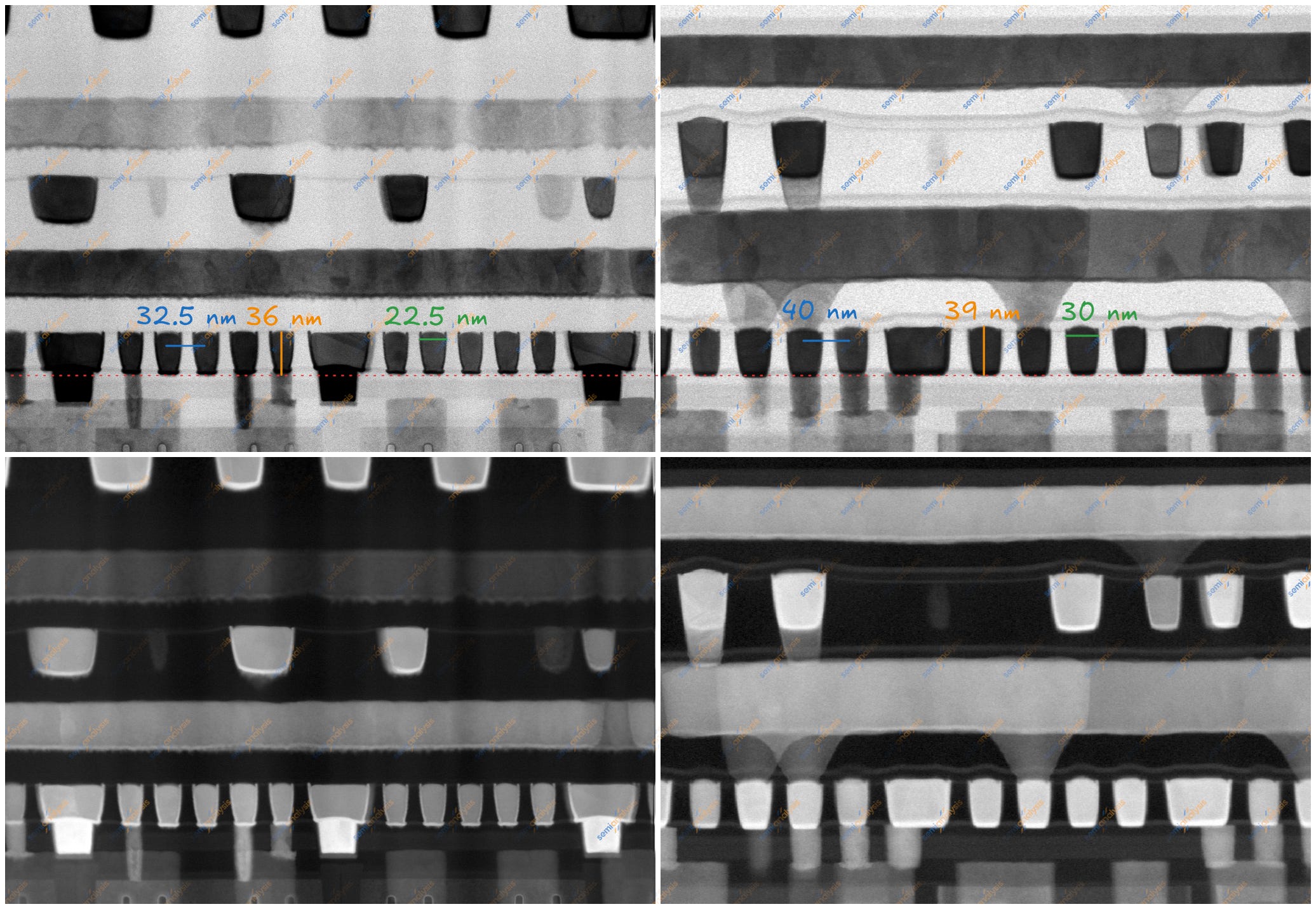
Standard Cell
A standard cell is the basic building block of chip layout: a fixed-height row pairing one NMOS and one PMOS transistor that share a gate, tiled in a grid to build logic blocks. The key dimensions are contacted gate pitch (CGP), cell height (CH), fin count, and the lower-metal routing grid.
To measure density, we use the Bohr metric: a weighted average of NAND2 gate area (60%) and scan flip-flop area (40%). This represents a realistic mix of combinational and sequential logic. This metric has its limitations, especially for complex cell layouts like TSMC’s FinFLEX, which alternates cells with different fin counts. Even so, it is the best metric for a pure process-level comparison.
Another important measurement is the fin pitch; it refers to the distance between two fins of the same transistor. In a FinFET process, multiple fins are used in each transistor to increase the drive current and thus performance.
TSMC N6 ships both a high-density (HD) library with 2 PMOS and 2 NMOS fins per cell, and a high-performance (HP) library with 3 of each. More fins under the shared gate mean more effective channel width. HP cells switch harder at the cost of area. Designers mix the two on a die, primarily spending HP cells on timing-critical paths, and matching their PPA targets.
In the Cortex-A55 core of the Helio G99, we found a cell height of 240 nm for the HD cell. MediaTek has used HD cells in the G99 to minimize die size and thus cost. As an SoC for budget smartphones at ~$100, this is essential.
By contrast, we found only one library in the Kirin 9030, with 2 NMOS and 2 PMOS fins. This suggests a narrower library strategy than TSMC N6, where both HD and HP libraries are widely used. This likely reflects the smaller customer base and the more constrained domestic design and electronic design automation (EDA) ecosystem.
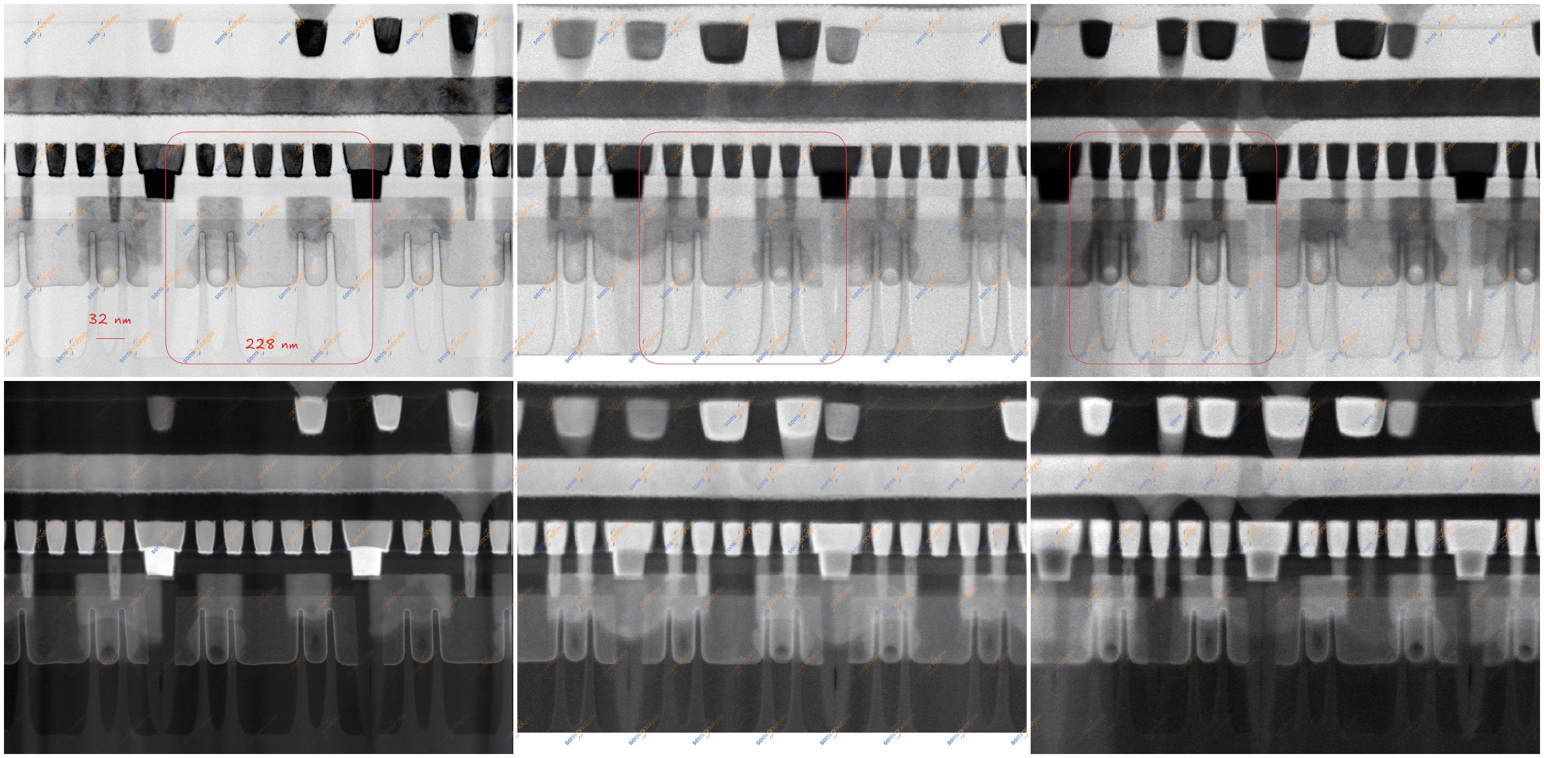
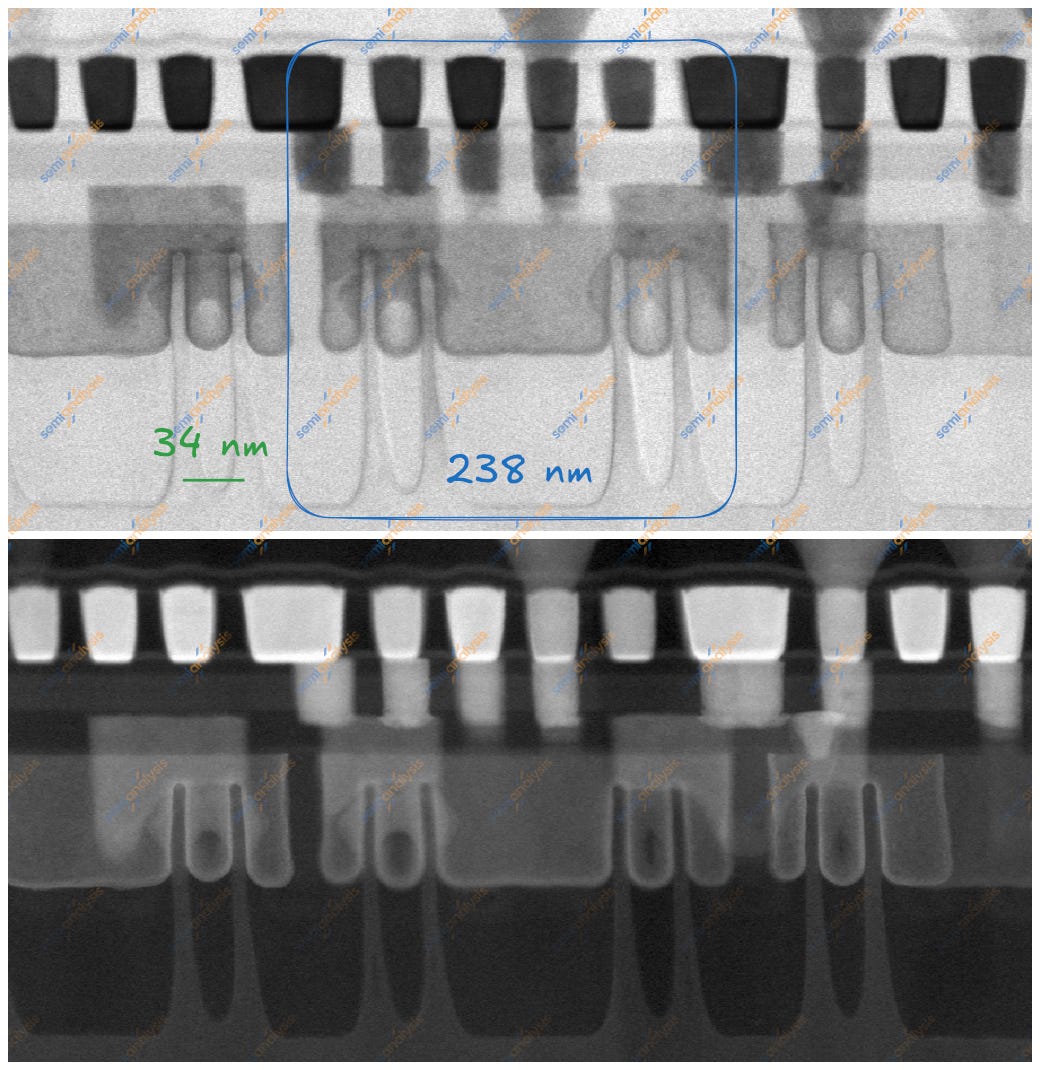
In all three CPU cores of the Kirin 9030, we found cell heights of 228 nm, 5% smaller than on N6. This is also a reduction of 9.5% over SMIC N+2’s cell height of 252 nm.
SMIC N+3 and TSMC N6’s HD library both feature a CGP of 57 nm. For SMIC, this is a 9.5% shrink over N+2.
In the past, CGP and cell height alone may have been enough to compare transistor density. Now, however, we must consider scaling boosters and DTCO as well. SMIC’s density gain does not come from EUV. It comes from using every available DTCO booster aggressively.
First is fin depopulation: reducing the number of NMOS and PMOS fins in each cell. The first FinFET nodes started with 3 or 4 fins for each transistor. SMIC N+3 and TSMC N6 HD both use only 2 fins per transistor, trading drive strength for density.
Next is contact over active gate (COAG). By landing the gate contact directly over the active gate, instead of out over the isolation region, the cell height drops. N+3 integrates COAG while N6 does not. Our N+3 gate-cut cross-sections indicate COAG, with the gate contact sitting over the active region, while N6 shows an off-gate contact.
Last is single diffusion break (SDB). Diffusion breaks are inserted between cells in the same row to provide electrical isolation, but they also introduce local layout effects (LLE), layout-dependent shifts in electrical characteristics. In the past, a double diffusion break was used, consuming the space of two CGPs. SMIC N+3 and TSMC N6 instead use SDB, saving area but increasing LLE sensitivity. This must be controlled at the process level and accurately modeled in the process design kit (PDK) so that EDA tools can account for it.
Overall, SMIC N+3 has a transistor density of 113.4 MTr/mm², slightly above TSMC N6 at 107.7 MTr/mm². Even without EUV, SMIC has achieved density beyond TSMC’s mature N6 node which utilizes EUV.
Metal Stack
The smallest critical dimension in the teardown is M0; SMIC N+3 uses a 32.5 nm local metal pitch. That is smaller than the 36 nm M0 pitch on Intel 18A in Panther Lake. However, this does not mean that SMIC has a better process than Intel 18A or TSMC N3P. M0 is a local intra-cell routing layer. Its usefulness depends on the full interconnect stack: M1 and M2 pitch, track count, via and line resistance, design rules, mask count, overlay control, and routing flexibility.
The 32.5 nm M0 is consistent with self-aligned quadruple patterning (SAQP), whose four-population line-width loading we read coarsely as alternating widths of 21.5 to 24 nm; M1 and M2, at 38 and 40 nm, are consistent with self-aligned double patterning (SADP), a single A/B split. On TSMC N6, M0, M2, and M3 sit at a relaxed ~40 nm and are consistent with SADP-class double patterning, with no need for quadruple patterning. That said, we measure M2 for example at ~43 nm, likely inflated by sparse routing. We do not assign any specific layer to EUV from our cross-sections; the distinction we can draw is double versus quadruple patterning, not lithography wavelength.
Transistor-level density in the front-end-of-line (FEOL) sets an upper bound, but the design is ultimately limited by what the interconnect stack can route. The lowest metals are the most important for standard-cell density, but the semi-global and global layers determine how usable that density is at the block and chip level.
Two axes are commonly used for chip cross-sections: the fin-cut and the gate-cut. The micrograph above is a fin-cut and shows metals 0 through 3. This axis lets us see the even-numbered metals, with M0 right above the fins.
There are two kinds of M0 lines. The first are the power rails; these are wide wires for the VDD and VSS running horizontally at the top and bottom edges of each standard cell. The wide wires measure 55 nm across, more than double the other M0 lines. Their width minimizes resistance and reduces IR drop. The second kind are intra-cell wires, short segments within the cell that connect terminals to M1. These have alternating widths between 21.5 and 24 nm.
The M0 pitch is 32.5 nm, a 19% reduction versus N+2 and N6. At this pitch, DUV patterning requires more aggressive multi-patterning, increasing mask count, overlay sensitivity, process complexity and cost.
M0 is below what a single DUV-defined spacer (SADP) can resolve, so SMIC cascades a second spacer step (SAQP). The cross-section reflects the cost: the M0 trenches are visibly more re-entrant (narrower at the bottom than the top) than M1 or M2 on the same chip and carry a bright barrier-rich foot where the trench meets the etch-stop layer. That shape is partly the intended damascene profile, as a slightly narrow bottom helps void-free copper fill, but its magnitude at M0 is driven by the tight pitch and the higher trench aspect ratio.
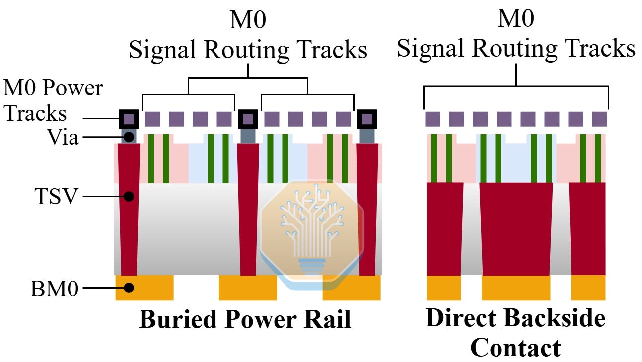
Intel 18A supports an M0 pitch of 32 nm, although Panther Lake has only shipped with a looser 36 nm pitch. This is due to Intel’s heavy usage of HP libraries. Among leading-edge nodes, 18A has the loosest M0 pitches due to PowerVia. With power routing moving to the backside, congestion is reduced, and the entire front-side metal stack can be used for signal routing.
M2 is the first true inter-cell routing layer. It runs horizontally like M0 but spans across multiple cells to carry block-level signals. The M2 pitch sets the cell’s track height – the number of M2 tracks that fit between the VDD and VSS rails, defining what the library calls a 6-track or 7.5-track cell. This layer is the most important, limiting the routing of entire blocks.
SMIC N+3 features a 5.7-track cell. The M2 pitch is 40 nm, a 5% decrease over N+2 and the same as N6. This shrink keeps the pitch at the edge of what is possible with double patterning. Future nodes will need to increase the number of masks for M2 as reducing the number of tracks is much harder due to the limitations in routing.
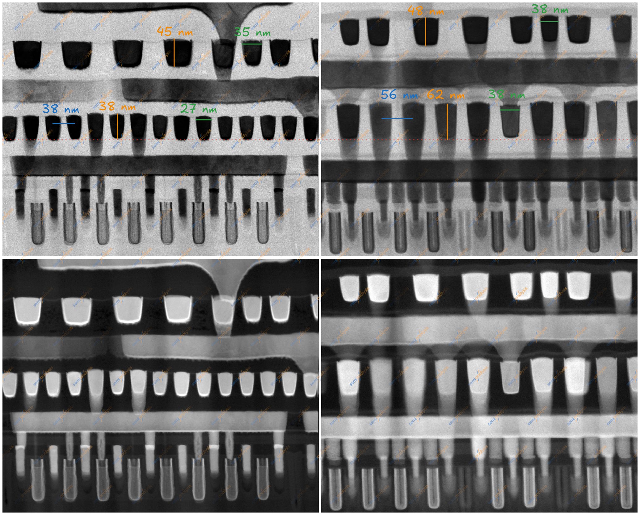
The micrograph above is in the perpendicular direction, the gate-cut, and shows metals 0 through 4. This allows us to see and measure the odd-numbered vertical metal layers.
The M1 pitch is 38 nm, 9.5% less than N+2 and 33% less than N6. The M1-to-gate ratio matters because it sets local routing flexibility. N+2 and N+3 use a 3:2 ratio, while N6 uses a 1:1 ratio, explaining the huge differences in M1 pitch. The more M1 lines there are compared with the gates, the more flexibility there is for power and signal crossing within the cell. Routing flexibility enables more complex and better cells. Clean fractional ratios are also preferred as a grid is periodic and improves layouts. The 3:2 ratio gives SMIC more local routing flexibility than a strict 1:1 grid, but it also complicates layout and patterning. This is a DTCO choice, with SMIC increasing process complexity to recover density and routability without EUV.
This 3:2 ratio is not very popular in the leading-edge nodes. TSMC has only used it on N7+, the N5 family, and the short-lived N3(B). They have switched back to a 1:1 ratio for N3E. Intel has only used it on the 10 nm/Intel 7 family, with Intel 4, 3 and 18A all using a 1:1 ratio. Samsung is the only one still using a 3:2 ratio at the leading edge, using it in the SF4 and SF3 families. It remains to be seen if SMIC will remain at a 3:2 ratio or move to a 1:1 ratio with its future nodes.
The industry is still actively exploring these local-routing ratios. At VLSI 2026, imec will be presenting work on even higher ratios, including a 2:1 scheme that can reduce area by up to 14%. We will be covering the conference in a future newsletter article.
We’re diving deep into the most advanced datacenter and AI hardware hitting the market. To learn more about what’s in the pipeline or to commission a custom teardown, contact sales@semianalysis.com. Interested in joining us on this ride and think you can be a difference maker? Check out our Careers page.
The final local interconnect layer for N+3 is M3, with a pitch of 44 nm. The M3 pitch is the same as on N+2 and 10% larger than on N6.
The semi-global layers carry the majority of block-level signal routing. They have a coarser pitch than the lower local layers. On leading-edge nodes, they are designed to sit at the limit of DUV single patterning.
M4 through M11 pitches were found divided between 80–82 nm (M4–M6), 128 nm (M7–M10), and 148 nm (M11). Given limited sampling, it is possible these are divided further in dense routing areas. At the top are two giant metal layers, M12 and M13. These have kept the same pitches as N+2 at 1920 nm and 4600 nm respectively.
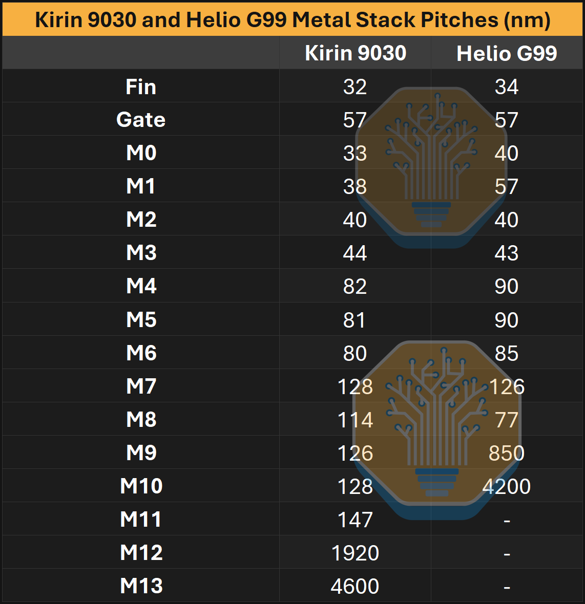
While the lower layers’ pitches are generally fixed by the process and library, the upper layers vary much more in pitch and count, depending on the design. Even two smartphone SoCs on the same process can have wildly different metal stacks. The Helio G99 carries fewer routing layers, reaching coarse metal pitches of 850 nm by M9, while the larger and higher-performance Kirin 9030 keeps fine pitches until M11.
SRAM
At the leading edge, SRAM is much more difficult to scale than logic. TSMC’s latest nodes have seen little to no bitcell scaling, while logic still has more DTCO levers to pull.
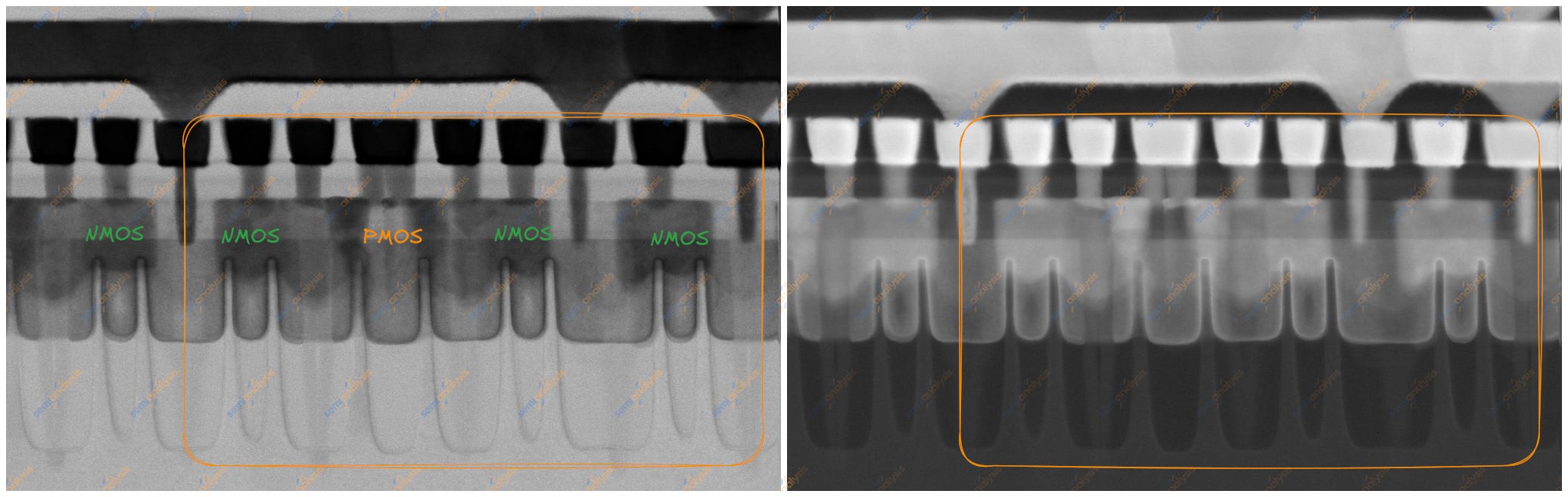
While looking for other logic libraries in the GPU compute units, we stumbled upon the SRAM. The most common type of SRAM has 6 transistors (6T), but this cell had 8 transistors (8T) instead.
8T SRAM adds two transistors to form a dedicated read port. Unlike a 6T cell, where reading disturbs the storage, the decoupled read port removes read-disturb, improving read stability and letting the cell be pushed harder for performance.
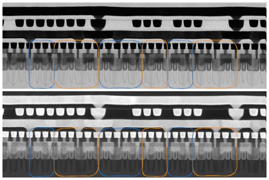
At first glance, the cut looked like an unusual logic library, with each cell row having 3 fins of one polarity and 5 fins of another. The rows also alternated in orientation.
Energy-dispersive X-ray spectroscopy (EDS) resolved our confusion. The cut had not landed on the GPU logic, but on the SRAM macro beside it. The unusual fin pattern was due to the SRAM library. We return to EDS in the process flow analysis behind the paywall.
SRAM libraries are not like traditional logic libraries. Due to the unequal number of PMOS and NMOS transistors, they require specialized rules and layout libraries. They do not need the flexibility of logic libraries, so they are hyper-optimized for one purpose: dense, reliable memory.
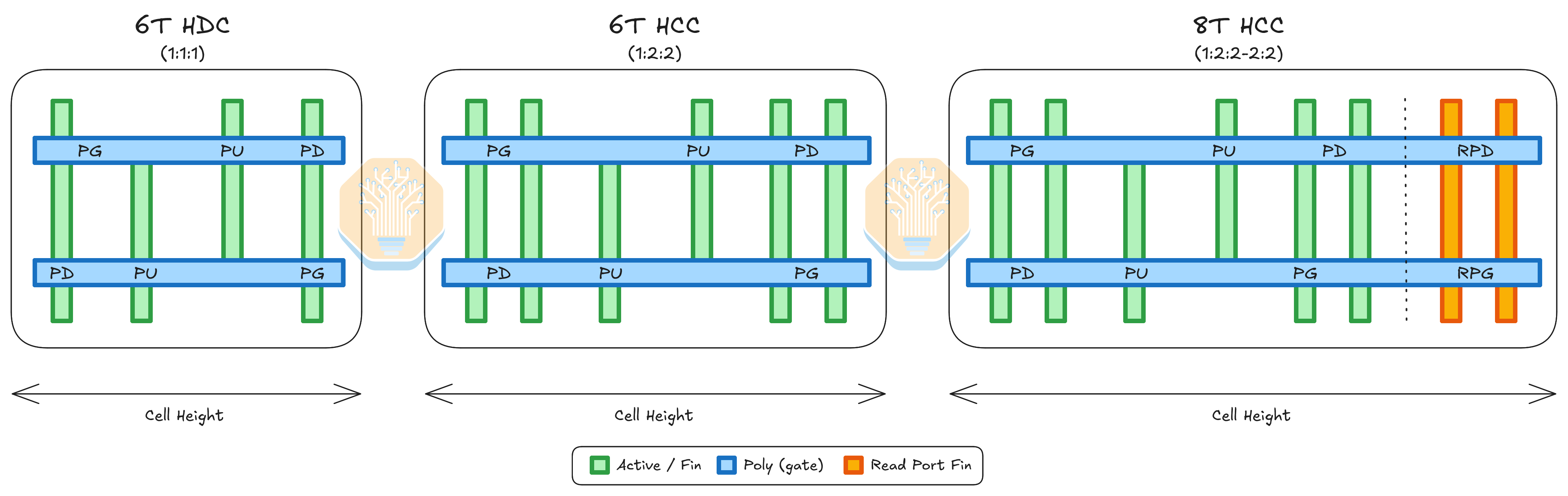
The SRAM cell we found is a 1:2:2-2:2 cell. This means there is 1 fin per pull-up (PU) PMOS transistor, and 2 fins per pull-down (PD) and pass-gate (PG) NMOS transistor. These 2 PU, 2 PD and 2 PG transistors would usually form a single 6T high-current cell (HCC). An 8T HCC adds a read-pull-down (RPD) and a read-pass-gate (RPG) NMOS transistor, each with two fins.
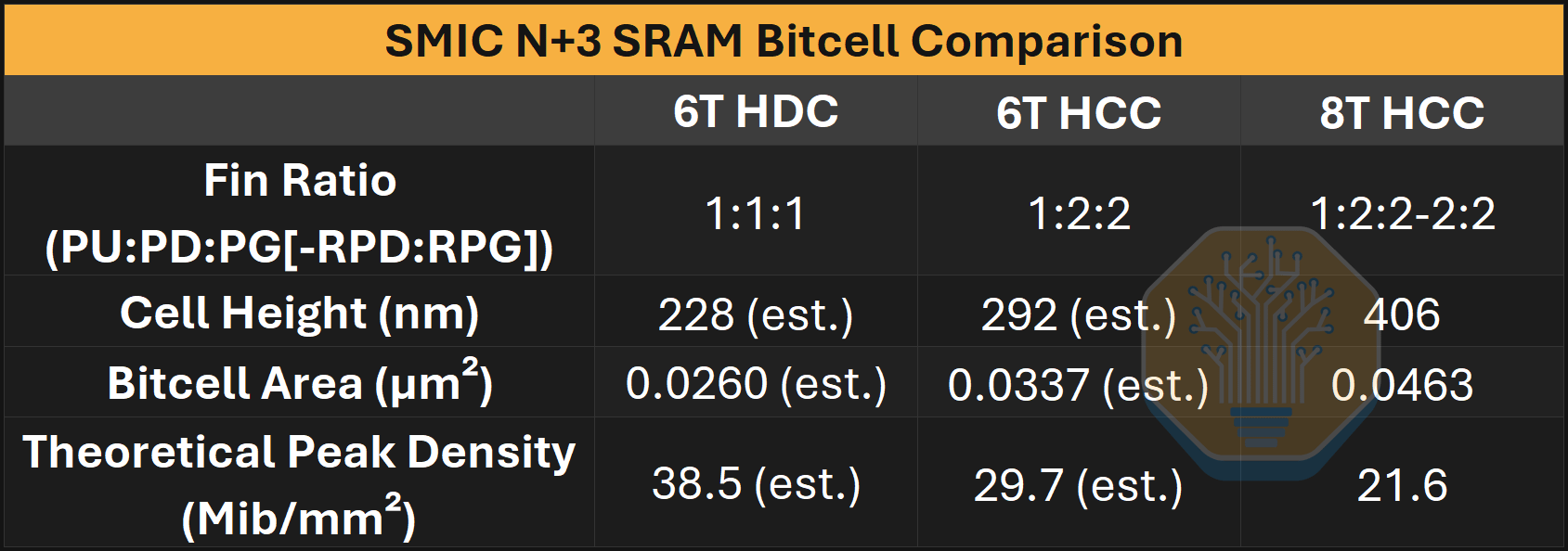
We measured a cell height of 406 nm, which brings the bitcell size to 0.0463 µm². That is a theoretical peak density of 21.6 Mib/mm². We estimate that a 6T HCC would have a cell height of 292 nm and a size of 0.0337 µm². This is ~12% larger than a 6T HCC on Intel 3 and 4.
We also estimate the 6T high-density cell (HDC) to have a cell height of 228 nm and a size of 0.0260 µm². This is coincidentally the same as the logic standard-cell height measured earlier. The estimate puts the cell near Samsung 7LPP/5LPP and slightly below TSMC N7/N6. That is a theoretical peak density of 38.5 Mib/mm². 6T HDC is arguably the most important cell as it is used for the largest caches in a chip, the L3 caches and system-level cache (SLC).
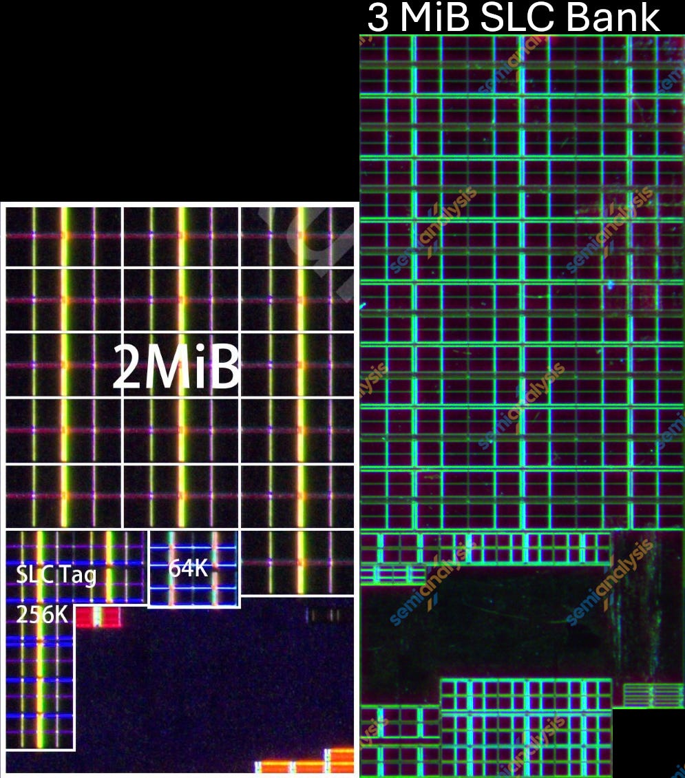
Both the Kirin 9020 and 9030 have split the SLC into 4 banks to raise total SLC bandwidth. In the Kirin 9030, the SLC increased from 2 MiB to 3 MiB per bank. Correspondingly, the number of arrays within the bank also increased by 50%, from 16 to 24. Each array can store 128 KiB and forms an orderly pattern on the die shot.
From the Kirin 9020 to the Kirin 9030, the area of a 128 KiB SLC array decreased from 0.0477 mm² to 0.0392 mm², an 18% shrink. The achieved density is 25.5 Mib/mm², 66% of the theoretical maximum.
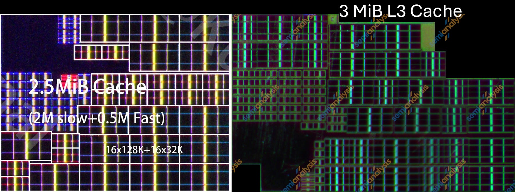
While the SLC was quite similar across both chips, the L3 has seen some major changes, particularly in terms of its layout. The total capacity also went up from 10 MiB to 12 MiB. Much like the SLC, the L3 is also split into 4 banks.
In the Kirin 9020, an L3 bank consisted of 16× 128 KiB arrays and 16× 32 KiB arrays. However, an L3 bank in the Kirin 9030 instead consists of 48× 64 KiB arrays.
In the Kirin 9020 L3, a 128 KiB array was 0.0513 mm² and a 32 KiB array was 0.0154 mm². The size of the 128 KiB array is different on the L3 and SLC as the assist circuitry for the two arrays differs depending on their purpose.
In the Kirin 9030 L3, a 64 KiB array is 0.0210 mm². Although not a like-for-like comparison, normalized for capacity, it is 18% smaller than the 9020’s 128 KiB L3 array and 31% smaller than its 32 KiB L3 array. The achieved density is slightly lower than the SLC, at 23.8 Mib/mm², 62% of the theoretical maximum.
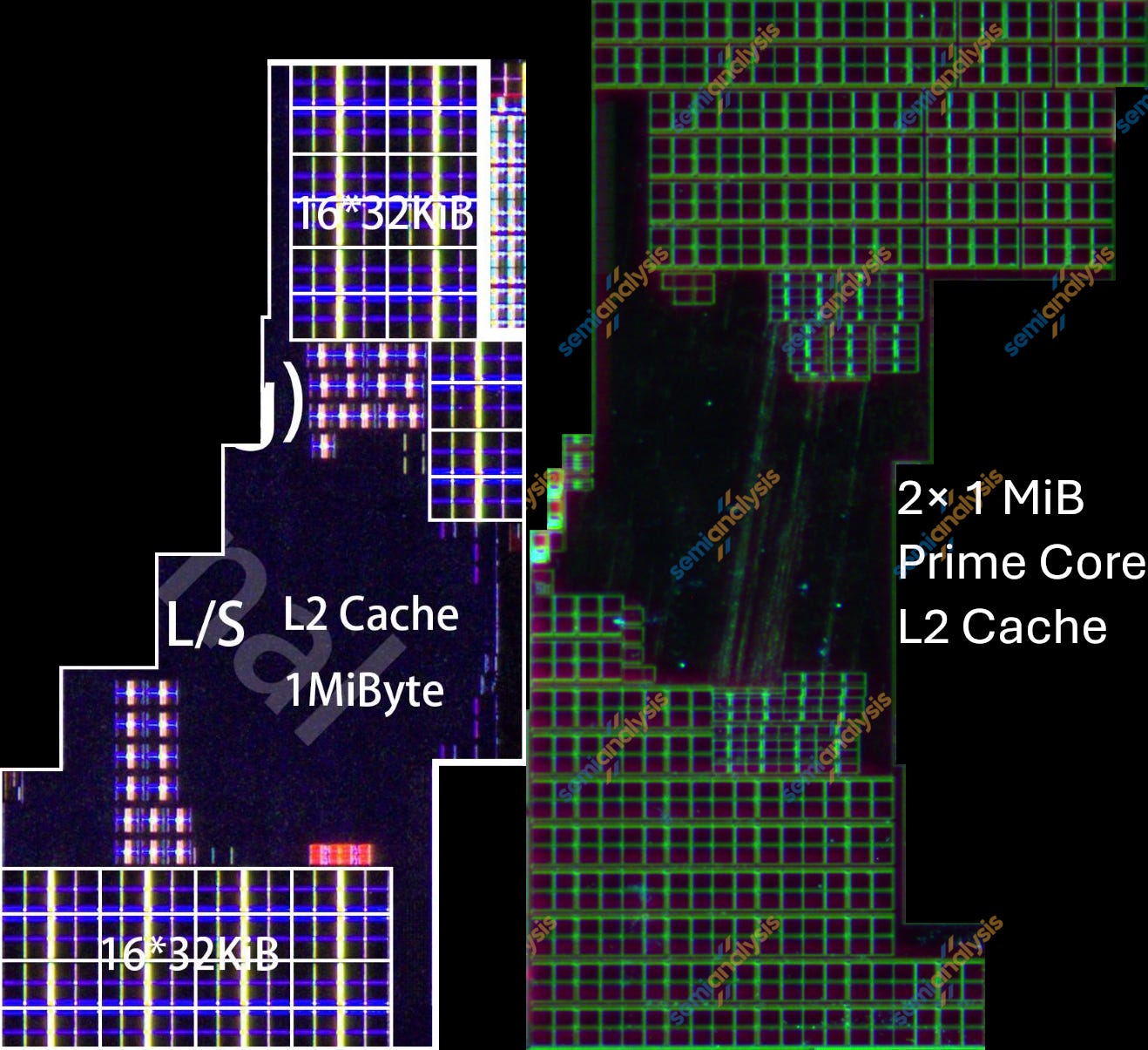
Unlike the L3 and SLC, the prime cores’ private L2 cache uses a 2-bank design. As the prime cores’ L2 is latency-critical, it likely uses 6T HCC instead of 6T HDC. The 9020 has 16 arrays in each bank while the 9030 has 32. Each array has a capacity of 32 KiB.
A 32 KiB array in the L2 shrank from 0.0171 mm² to 0.0142 mm², ~17% smaller. The density is 17.6 Mib/mm², ~59% of the theoretical maximum for 6T HCC.
SRAM scaled well from N+2 to N+3, shrinking by ~19%, close to the theoretical logic shrink. The caveat is that N+2’s bitcells were unusually large, bigger than comparable 7 nm-class nodes, so part of the gain is catch-up rather than true scaling.
With the insights from STEEL’s teardowns, we will be doing a deep dive into SRAM in a future newsletter article.
Everything above came out of a single STEEL teardown: die annotation, block-level area analysis and TEM cross-sections through logic and SRAM. We’re diving deep into the most advanced datacenter and AI hardware hitting the market. To learn more about what’s in the pipeline or to commission a custom teardown, contact sales@semianalysis.com.
Future Roadmap
The same cross-sections that pin down N+3 also show where SMIC can go next. Although N+3 is already close to the practical limits of DUV multi-patterning in several layers, SMIC still has a few scaling levers left.
A theoretical N+4 would likely start with cell height. N+3 uses 5 M0 tracks between its power rails. Moving to 4 M0 tracks, as on SMIC N+2 and TSMC N6, could reduce cell height by roughly 15%. The routing grid is only one side of the shrink; the front end also must fit into the smaller cell.
One possible FEOL lever is reducing the p-to-n isolation spacing from two diffusion grid units to one. Intel used this scaling booster on Intel 4, and TSMC did so on its N3 family. This path trades layout flexibility for density. Fewer M0 tracks reduce local routing resources, while tighter p-to-n spacing raises integration and design-rule difficulty.
M2 is also constrained by the cell height shrink. For SMIC to maintain a ~5.7-track cell, M2 would need to move toward ~35 nm. That would move another layer into SAQP territory.
SMIC could also reduce the CGP from 57 nm to 54 nm. Intel reached a similar CGP on Intel 10 nm/Intel 7 without EUV. The local interconnect is also tougher. If SMIC keeps the 3:2 M1-to-gate ratio, M1 would need to shrink to 36 nm and would likely require SAQP as well. If SMIC moves to a 1:1 ratio, M1 could relax to 54 nm, but it would give up routing flexibility.
Under this theoretical path, we estimate that SMIC N+4 could reach a cell height of 198 nm and a CGP of 54 nm, implying a Bohr density of 137.8 MTr/mm², on par with TSMC N5 or Samsung SF4. However, the difficulty is cumulative. Each step is individually plausible, but together they make N+4 harder than the transition from N+2 to N+3. It will likely take longer, cost more, and carry less process margin.
A theoretical N+5 would require a larger integration shift. One possible path is backside contacts (BSCon), moving power routing and source/drain contacts to the backside, which would reduce front-side routing pressure and enable another reduction in cell height.
The front-side metal pitches could relax to reduce the process complexity. M0 would likely relax slightly to ~34 nm, and M2 and M4 pitches could relax further. CGP is unlikely to shrink much further. Even with EUV, 48 nm has been the practical limit for yield and process control.
This approach would allow N+5’s cell height to fall to 170 nm and its CGP to 53 nm. This implies a Bohr density of 163.6 MTr/mm², on par with Intel 18A’s HP library. However, this would not make N+5 cost-competitive with the leading edge. It would reach a similar density through a much more expensive route. The integration difficulty rises sharply, with new process flows for backside alignment, wafer thinning, contact reveal, and backside metallization.
Past this point, standard density and interconnect scaling become increasingly unattractive. That is where Huawei’s roadmap stops looking like a normal foundry roadmap and starts looking like a packaging roadmap.
Huawei’s τ Scaling Law
At ISCAS 2026, Huawei unveiled its tau (τ) scaling law, reframing process scaling in the time domain. τ is the time cost of data movement and processing: switching delays in transistors, RC signal propagation delays in circuits, compute, memory, and networking latency. Outside Huawei’s terminology, this is called system-technology co-optimization.
This is Huawei’s answer to its lack of EUV lithography. Without EUV, planar density cannot keep pace with TSMC, Intel, or Samsung. If transistor density cannot shrink further, Huawei’s alternative is to shorten wires, reduce buffering, and stack logic vertically.
“LogicFolding”, Huawei’s implementation of this new scaling idea, is, in practice, an aggressive 3D stacking approach. AMD V-Cache places SRAM above or below a CPU die. AMD’s MI350X places active interposer dies (AIDs) underneath accelerator and compute dies (XCDs), with the AIDs handling cache, IO interfaces, the network-on-chip (NoC) and embedded metal-insulator-metal (MIM) capacitors. With LogicFolding, parts of the same logic block are split across multiple active dies bonded face-to-face at ultra-fine pitch. This allows Huawei to shorten some critical paths and reduce buffer overhead, not merely add cache capacity or offload the IO and interconnect.
Shortening wires is where the higher clocks come from. A large share of a modern core’s delay and energy budget goes into driving long interconnects and the repeater buffers along them. LogicFolding distributes a block’s critical-path gates across multiple stacked tiers bonded at a very fine pitch, so the bond interface behaves like an additional metal layer and the longest paths get shorter. That is how Huawei expects to recover frequency and efficiency it cannot get from the process alone.
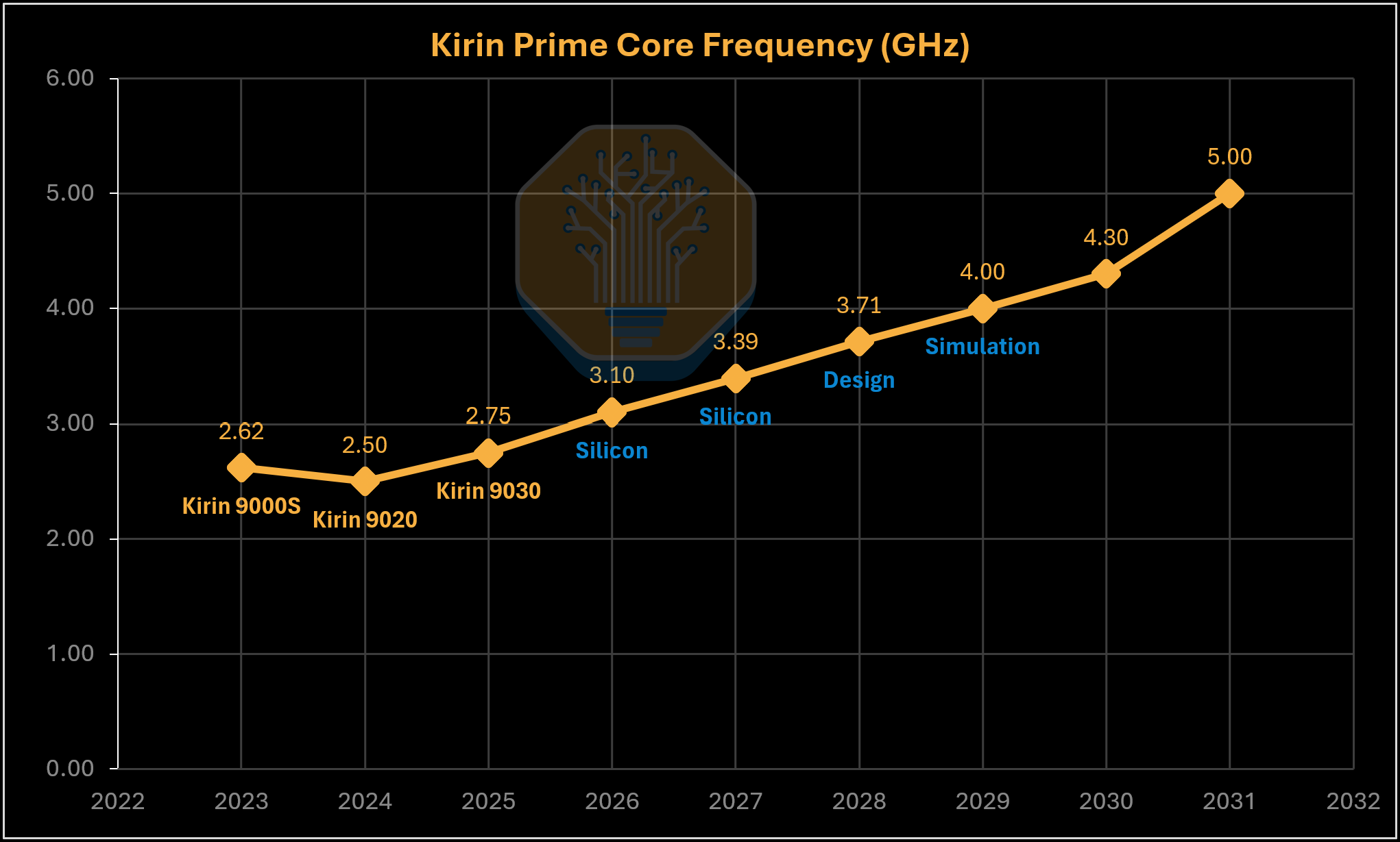
Huawei’s roadmap shows its intent. Prime core frequency is targeted to rise from 2.75 GHz in the Kirin 9030 to roughly 5 GHz by 2031, far beyond what planar scaling alone could deliver. Prime cores with 3.1 and 3.39 GHz clocks are being tested in its labs, although their power consumption is unknown. Beyond that, chips are in the design, simulation or pathfinding phase, meaning the frequencies are targets. However, the direction matters more: LogicFolding also helps with performance, not just density.
The catch is that Huawei’s density claim is not directly comparable to foundry densities. A stacked design can report more transistors per package footprint by adding active layers, even if each patterned die remains well behind TSMC or Intel in front-end density. This is how Huawei can claim to reach foundry 14A-equivalent density by 2031.
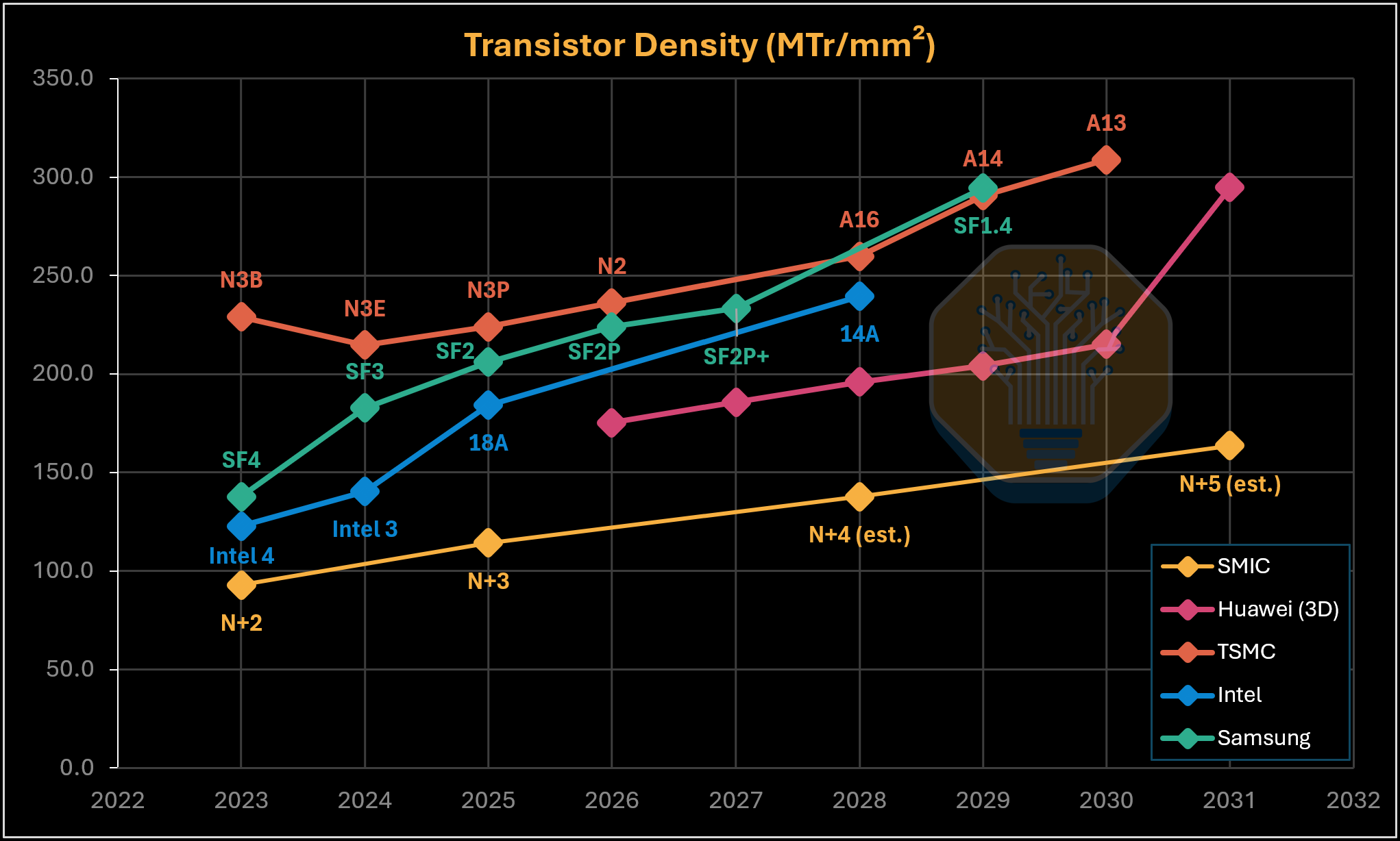
This is not a like-for-like foundry comparison, with Huawei using stacked logic and measuring density per package footprint. On a normalized Bohr-density basis, SMIC N+3 is ~114 MTr/mm², 38% less than Intel 18A’s HD library. Huawei’s 3D roadmap closes the gap by stacking active logic, reaching 215 MTr/mm² by 2030. In 2031, the roadmap density jumps to 295 MTr/mm², implying either a third active layer, partial EUV insertion or aggressive planar DUV scaling.
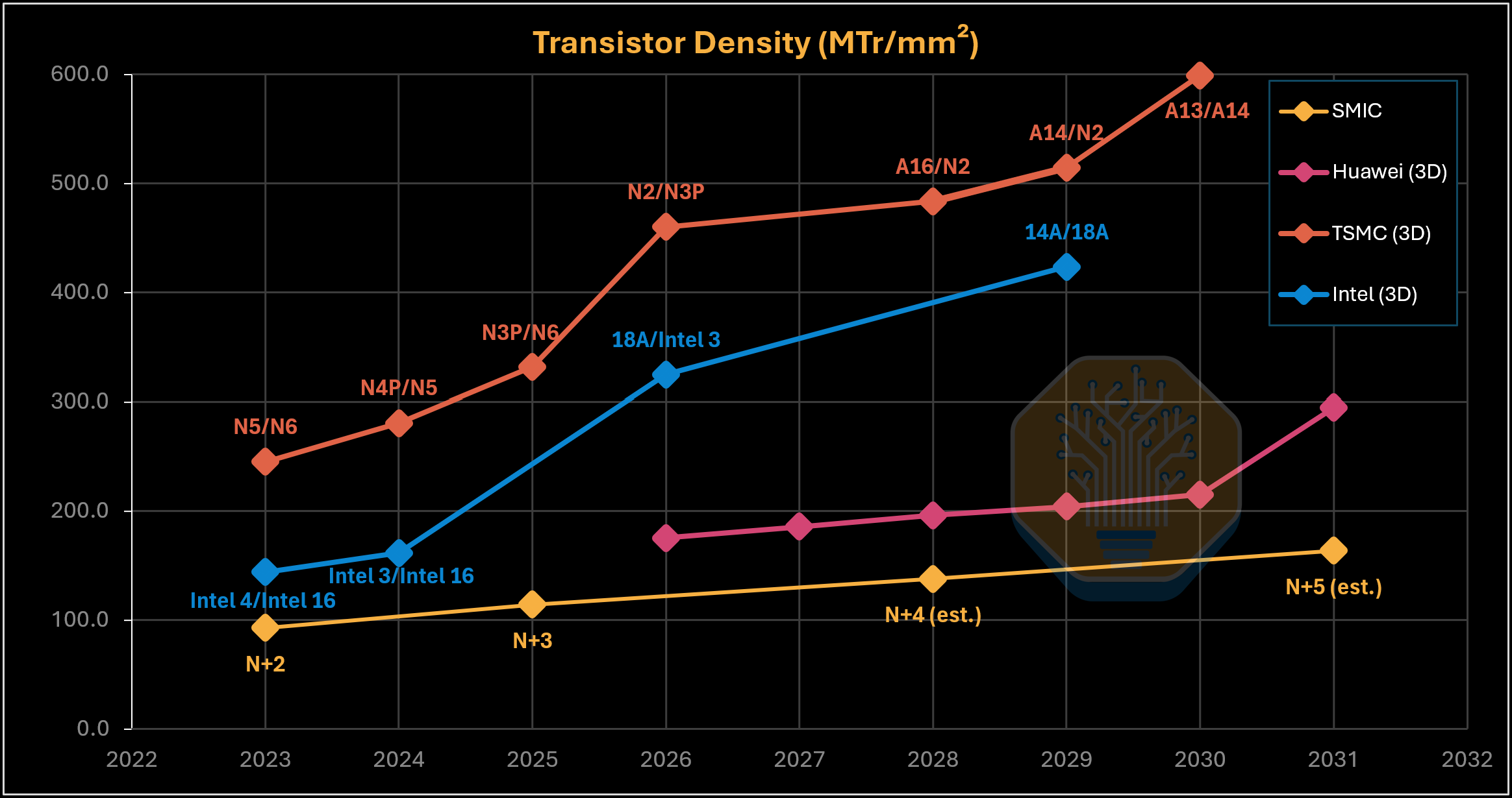
Huawei’s methodology makes other foundries look much denser as well. Applying it to AMD’s MI450X with an N2 top die on an N3P base die yields a theoretical density of 460.2 MTr/mm² in 2026, compared with Huawei’s 295 MTr/mm² in 2031.
This Kirin 9030 does not use LogicFolding, remaining in a conventional mobile SoC package. Instead, it forms the baseline for how far Huawei and SMIC can push planar scaling. Future teardowns of Kirin and Ascend chips will show both planar logic density and Huawei’s hybrid bonding solutions.
Export Controls & Future Scaling
Export controls changed China’s optimization problem rather than ending it. EUV restrictions raised the cost and complexity of leading-edge manufacturing without freezing it. SMIC reaches N6-class logic density through DUV immersion, SAQP and DTCO, while Huawei shifts more of the burden onto architecture, packaging and system-level integration.
Future nodes will be tougher. N+3 still had room to tighten local metals and reduce cell height and CGP. Further scaling without EUV leaves fewer levers. More aggressive multi-patterning adds masks and overlay error. SMIC can keep pushing DUV, but each step will get more expensive and less forgiving.
The design side is just as critical. Huawei had domestic EDA tools and flows before the Kirin 9030, with the Kirin 9000s, 9010 and 9020 making that clear. Huawei was able to ship multiple consumer SoCs on SMIC N+2 and N+3 while cut off from the Western EDA stack.
US export controls restricted EDA tools for advanced chips in 2022 but did not target tools for more mature chips. In 2025, the US government briefly placed much broader restrictions on EDA software from Synopsys, Cadence, and others, before lifting them less than two months later as part of a trade deal tied to rare earths. Huawei has been unable to access those tools because it remains on a US trade blacklist.
That forced Huawei, SMIC and Chinese academic institutions to build their own tools and flows. Researchers at Peking University recently announced a prototype EDA tool for Huawei’s LogicFolding architecture, which requires a new flow to handle the multilayer layout and floorplan. This is not the same as replacing the full Synopsys or Cadence stack, but it shows where domestic EDA is headed: toward tighter co-optimization between architecture, process and packaging.
These advances are also diffusing into the Chinese ecosystem. SMIC is licensing its N+2 and N+3 processes to HLMC/Hua Hong at the government’s direction rather than by choice. If the same process learning feeds into Ascend accelerators for AI training and inference, the choke point shifts from one named fab to an ecosystem. Alibaba’s T-Head silicon arm and Cambricon, a Chinese AI chip designer that is expected to supply ByteDance, could also be major beneficiaries. Sanctions aimed at SMIC alone become less effective once the manufacturing knowledge has spread to other fabs and design houses.
China is not closing the gap with Intel, Samsung and TSMC. The teardown shows the opposite in several places: no EUV, no backside power, higher process complexity, and visible trade-offs.
But China is still advancing. If domestic chips become good enough for phones, inference, networking and security-sensitive workloads, they can matter strategically without matching TSMC at the leading edge.
Behind the paywall, we show what else STEEL can do, with material and process flow analysis of SMIC N+3, and analysis of the Kirin 9030 package.
We’re diving deep into the most advanced datacenter and AI hardware hitting the market. To learn more about what’s in the pipeline, access the full Kirin 9030 and SMIC N+3 analysis or to commission a custom teardown, contact sales@semianalysis.com.