

ISSCC 2026: NVIDIA & Broadcom CPO, HBM4 & LPDDR6, TSMC Active LSI, Logic-Based SRAM, UCIe-S and More
ISSCC 2026 Roundup
There are three major semiconductor conferences each year, IEDM, VLSI and finally ISSCC. We have covered the former two in great detail over the past few years. Today, we finally complete the trinity with our roundup on ISSCC 2026.
Compared to IEDM and VLSI, ISSCC has a much bigger focus on integration and circuits. Almost every paper comes with some form of circuit diagram, together with clear measurements and data.
In past years, ISSCC findings have been hit or miss when it comes to industry impact. This year was different, a significant number of papers and presentations were directly relevant to market trends. Topics covered range from the latest advancements in HBM4, LPDDR6, GDDR7, and NAND, to co-packaged optics, advanced die-to-die interfaces, and advanced processors from the likes of MediaTek, AMD, Nvidia, and Microsoft.
In this roundup, we will cover major categories such as Memory, Optical Networking, High-Speed Electrical Interconnects, Processors.
Memory
One key theme that caught our attention at this year’s ISSCC was memory, including Samsung HBM4, Samsung and SK Hynix LPDDR6, and SK Hynix GDDR7. Other than DRAM, logic-based SRAM and MRAM also piqued our interest.
Samsung HBM4 - Paper 15.6
Samsung was the only one among the top three memory vendors to present a technical paper on HBM4. Before ISSCC, we noted in our Accelerator & HBM model that Samsung had made great improvements in their HBM4 generation over their HBM3E. The data presented at ISSCC confirmed our analysis, with Samsung posting best-in-class performance - we have also detailed this development months ago, in a model update note.
The technical details presented at ISSCC, combined with industry chatter we have gathered, clearly demonstrate that Samsung’s HBM4 is competitive with its peers. Notably, it can meet the pin speed required for Rubin while staying below 1V. While Samsung still lags SK Hynix in terms of reliability and stability, the company has made meaningful progress in closing the gap on the technology front and could challenge SK Hynix’s dominance in HBM. Their 1c-based HBM4 paired with an SF4 logic base die appears to deliver stronger performance in pin speed.
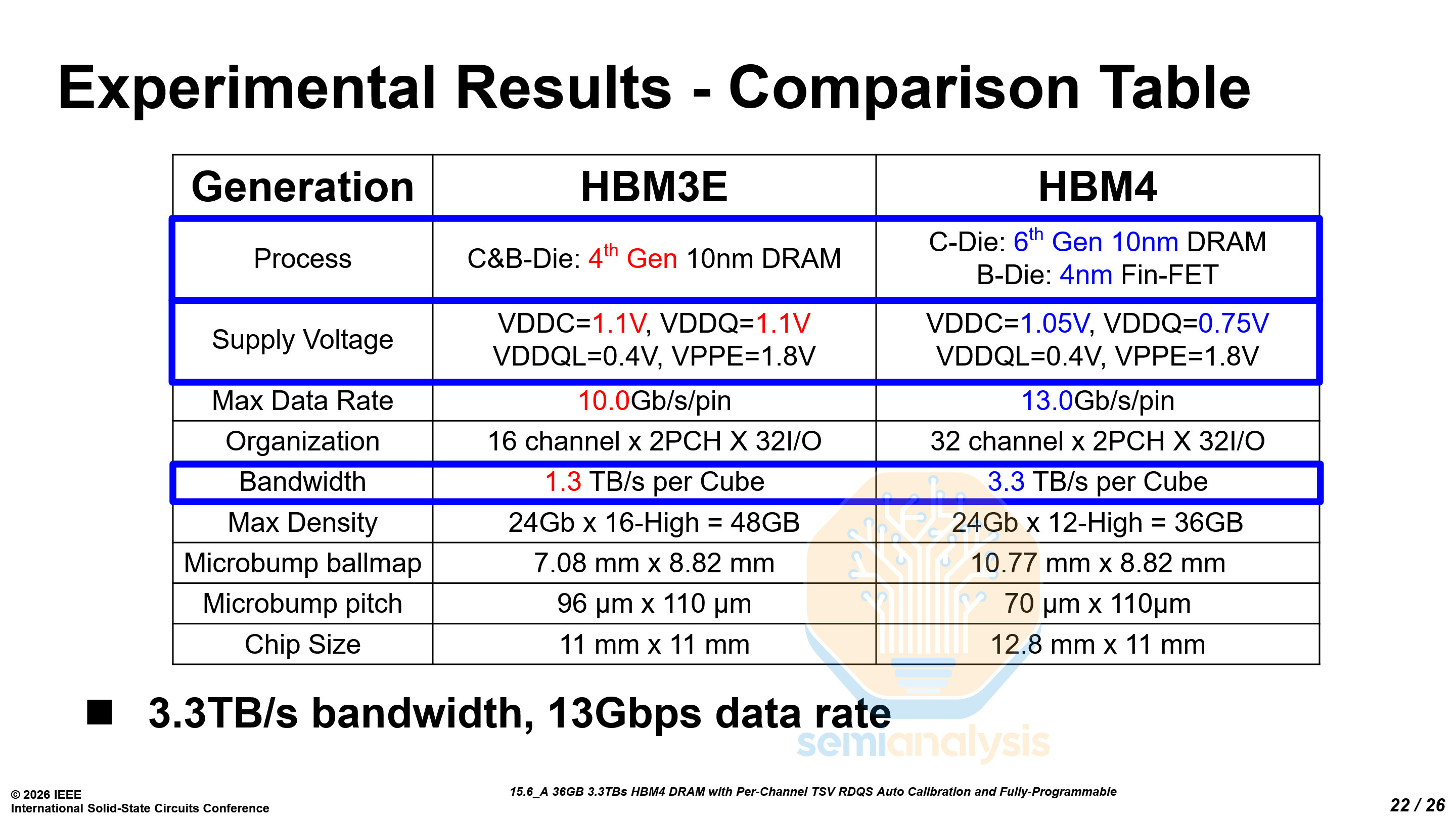
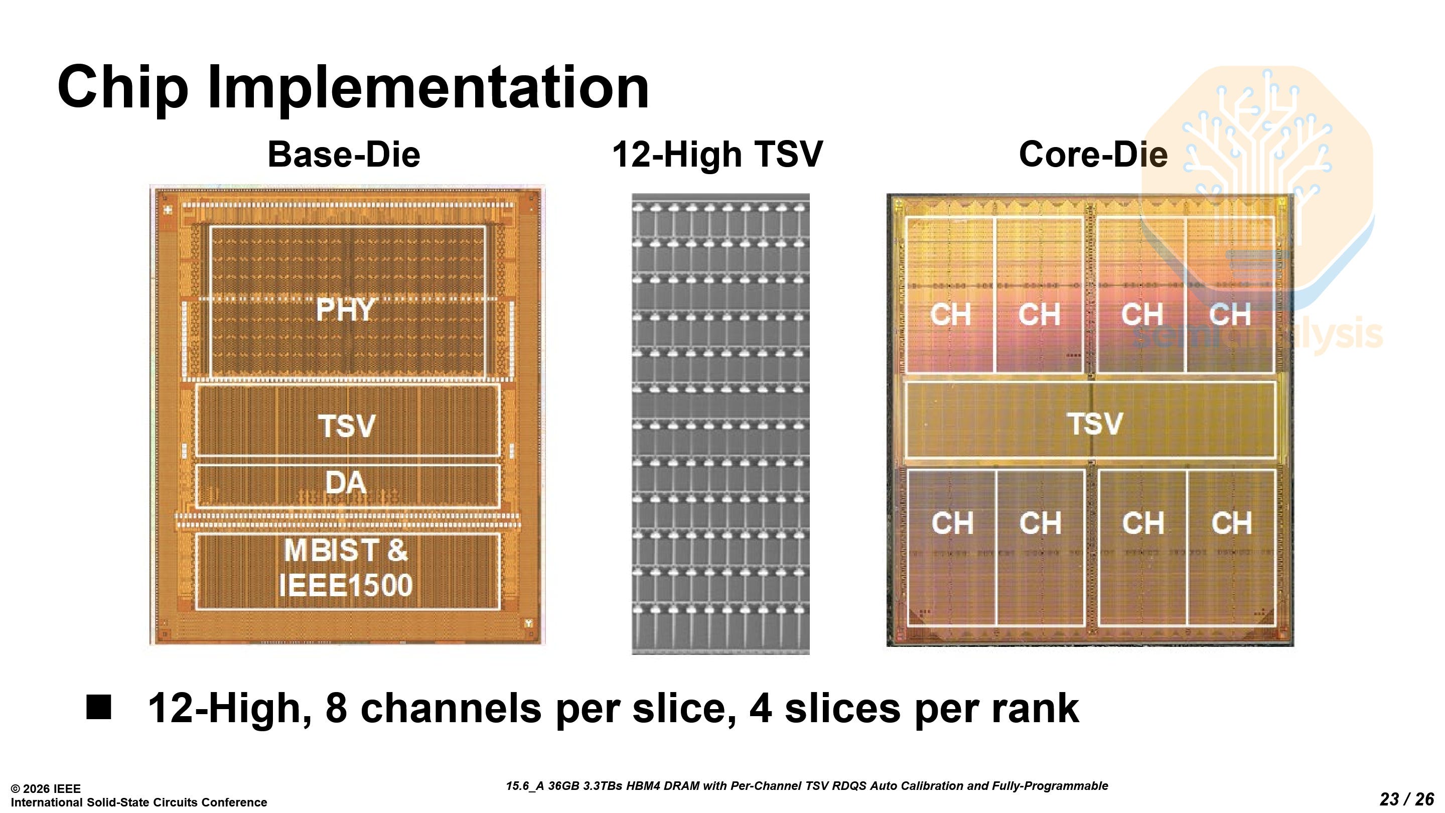
Samsung demonstrated a 36 GB, 12-high HBM4 stack featuring 2048 IO pins and 3.3 TB/s of bandwidth, built using 6th-generation 10nm-class (1c) DRAM core dies paired with an SF4 logic base die.
The most obvious architectural change from HBM3E to HBM4 is the process technology split between the core DRAM dies and the base die. HBM4 uses the DRAM process node only for the core die while the base die is manufactured with an advanced logic node unlike previous generations of HBM that used the same process for both.
The key architectural challenge arises as AI workloads demand higher bandwidth and faster data rates from HBM. By moving the base die to the SF4 logic process, Samsung enables higher operating speeds and lower power consumption. The operating voltage (VDDQ) fell 32%, from 1.1V in HBM3E to 0.75V in HBM4. A logic-based base die provides higher transistor density, smaller device dimensions, and better area efficiency due to smaller transistors and larger metal-layer stack availability as compared to a base die fabricated on a DRAM process. This helps Samsung’s HBM4 achieve — and significantly surpass — JEDEC’s HBM4 standard that we explain more at the end of this section.
Combined with adaptive body-bias (ABB) control, which mitigates process variation across stacked core dies, the doubled TSV counts further improve timing margin. Together, Samsung’s paper claimed that the ABB and the 4× higher TSV count allow their HBM4 to achieve operating speeds up to 13 Gb/s per pin.
The improvement brought by the SF4 base die and 1c DRAM core dies comes with a trade-off. Samsung’s choice of SF4 for the logic base die comes at a higher cost compared with competing approaches even though Samsung Foundry can offer discounts for their internal base die usage. SK Hynix is adopting TSMC’s N12 logic process for their HBM4 base die, while Micron relies on their internal CMOS base-die technology, both of which are lower-cost options than the near leading-edge SF4 node, even considering vertical integration cost advantages.
The 1c front-end manufacturing process has proved challenging for Samsung throughout 2025, especially given that the company skipped the 1b node and moved directly from 1a-based HBM3E to the 1c generation. Front-end yields for the 1c node were only around 50% last year, although they have been gradually improving over time. The lower yield poses a risk for their HBM4 margins.
Historically, Samsung’s HBM has earned lower margins than those of their top competitor, SK Hynix, a dynamic that we model across all vendors comprehensively in our Memory Model. We have detailed wafer volumes, yields, density, COGS, and more for each vendors HBM, DDR, and LPDDR across various nodes.
Samsung’s strategy appears to be an aggressive adoption of a more advanced node for the base die to achieve superior performance and outpace their competitors, particularly as HBM requirements from leading customers such as NVIDIA continue to become more demanding.
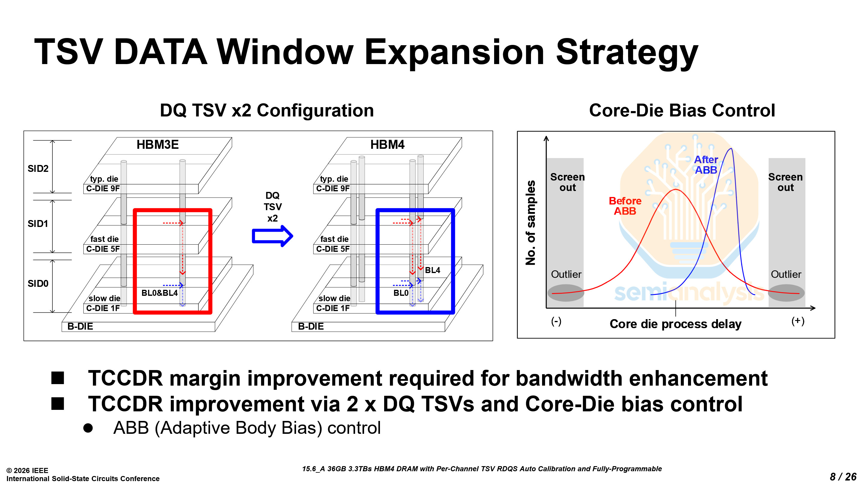
Another key issue in HBM to address is tCCDR, the minimum interval required between consecutive READ commands issued across different stack IDs (SID). For AI workloads that rely heavily on parallel memory access across many channels, tCCDR directly impacts achievable memory throughput.
In a stacked DRAM architecture, multiple core dies are vertically integrated on top of a base die. This naturally introduces small delay differences across the stack, driven by factors such as process variation between the core dies and the base die, TSV propagation differences, and local channel variation.
The increased stack heights and channel counts, from 16 to 32, compound this challenge. As the channel counts and stack heights increase, the variation between the dies accumulates, causing larger timing mismatches across channels and dies that impact the achievable tCCDR and overall HBM performance.
To address this issue, Samsung introduces a “per-channel TSV RDQS timing auto-calibration scheme.” After power-up, the system measures delay variation across channels using a replica RDQS path that mirrors the timing behavior of the real signal path. A time-to-digital converter (TDC) quantizes the timing differences, which are then compensated for using delay compensation circuits (DCDL) for each channel.
This calibration accounts for both global delay variation between stacked core dies and local per-channel variation, aligning timing across the stack. By compensating for these mismatches, Samsung significantly improves the effective timing margin and increases the maximum achievable data rate while maintaining the required tCCDR constraints. This scheme alone increased data rates from 7.8 Gb/s to 9.4 Gb/s.
Some of our readers who are well versed in memory technology may be asking: How is there enough die area to accommodate the significant increase in TSV counts? This is where the 1c node becomes important. Compared with the previous 1a node, 1c further shrinks the DRAM cell area, freeing up die space that can be used to integrate the larger number of TSVs required for HBM4.
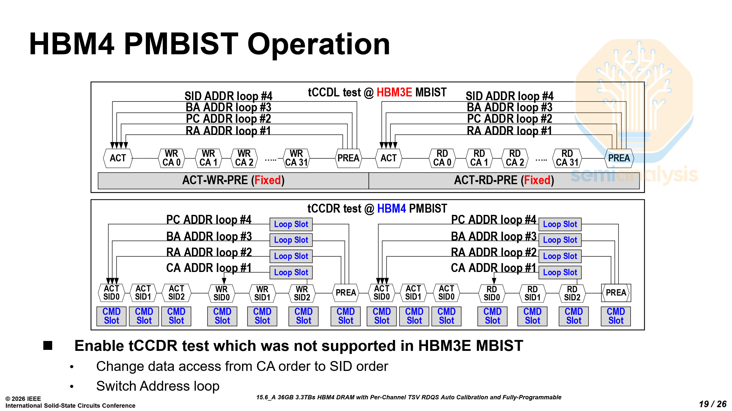
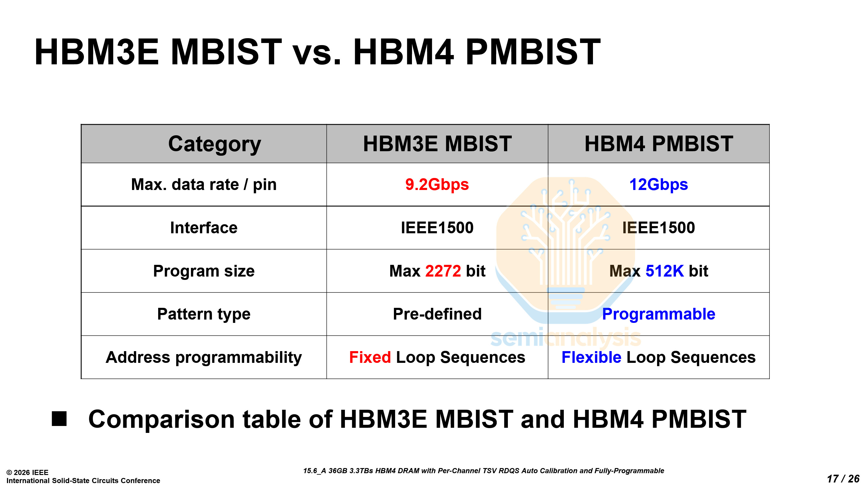
Another key innovation enabled by the logic base die is Samsung’s Programmable Memory Built-In Self-Test (PMBIST) architecture. PMBIST allows the base die to generate fully programmable memory test patterns while supporting the complete JEDEC row and column command set, meaning the test engine can issue the same commands that a real system would generate and can do so at any clock edge and at full interface speed. In practical terms, this allows engineers to replicate complex real-world memory access patterns and stress the HBM interface under realistic operating conditions, which is difficult with traditional fixed-pattern test engines.
This approach represents a notable departure from HBM3E. As discussed earlier, the HBM3E base die is fabricated using a DRAM process, which imposed strict power and area constraints on the MBIST (Memory Built-In Self-Test) engine and limited testing to a small set of predefined patterns given the natural power and area disadvantage of DRAM against logic. By moving the base die to Samsung Foundry’s SF4 logic process, Samsung enables a fully programmable testing framework capable of running complex test algorithms and flexible access sequences.
This enables much more robust debugging and better yield learning for HBM. Engineers can create targeted stress patterns to validate critical timing parameters such as tCCDR and tCCDS, identify corner-case failures earlier in manufacturing, and accelerate characterization during chip-on-wafer (CoW) and system-in-package (SiP) testing. Put simply, PMBIST improves test coverage, debug efficiency, and ultimately production yield as HBM stacks grow more complex and operate at higher speeds.
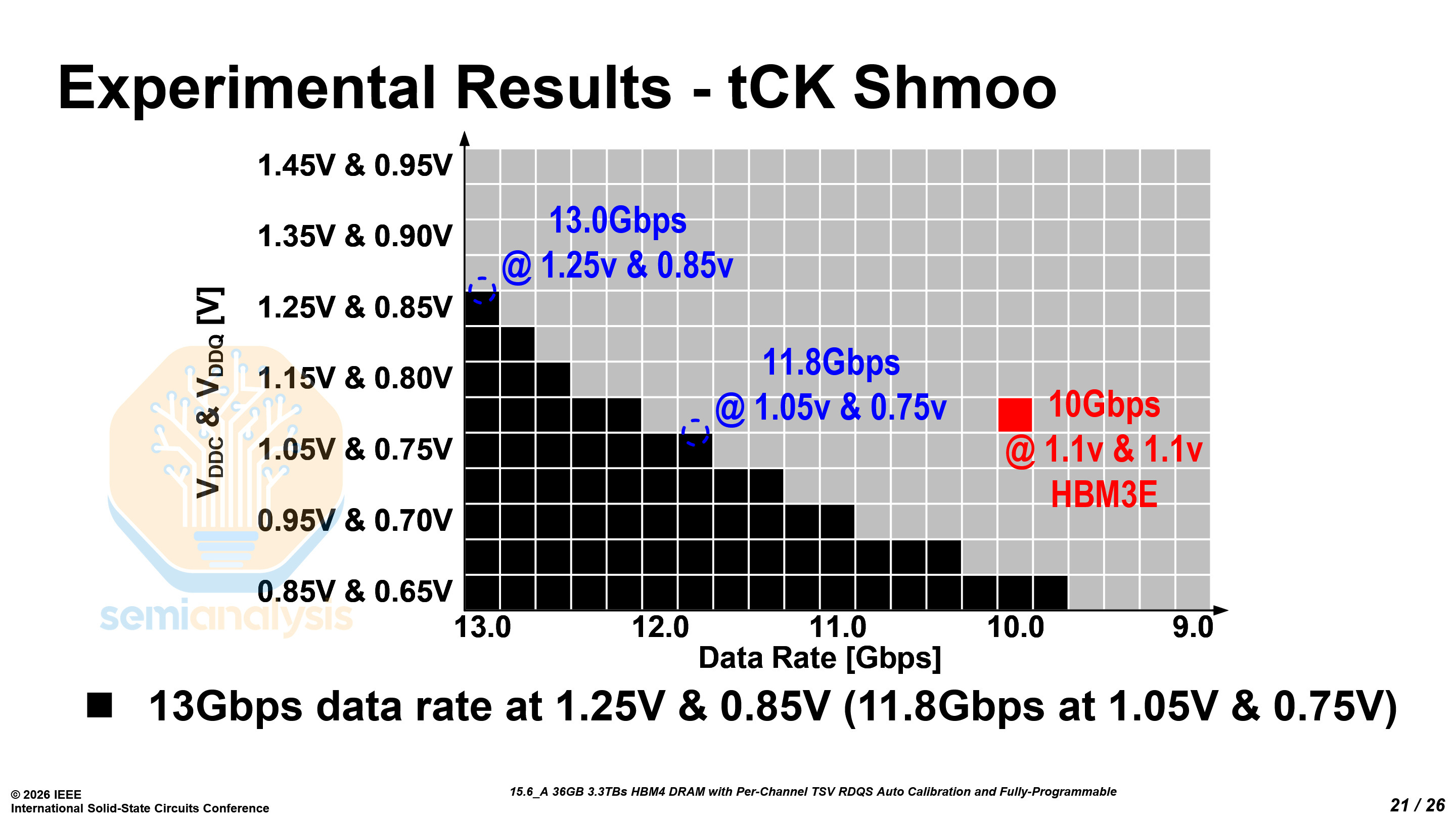
Samsung also demonstrated strong pin speed results — their HBM4 is able to hit 11 Gb/s at sub-1V core voltage (VDDC), and up to 13 Gb/s at higher voltages. We have yet to see Samsung’s peers demonstrate comparable performance albeit they do have better reliability and stability.
Samsung’s implementation significantly exceeds the baseline specification of the official JEDEC HBM4 standard (JESD270-4), which specifies a maximum data rate of 6.4 Gb/s per pin and about 2 TB/s of bandwidth. Samsung demonstrates more than 2× the JEDEC-standard pin speed, reaching 13 Gb/s per pin and delivering 3.3 TB/s of bandwidth. Even at VDDC/VDDQ of 1.05V and 0.75V, the device can sustain a data rate of 11.8 Gb/s.
Samsung LPDDR6 - Paper 15.8
Both Samsung and SK Hynix showed off their LPDDR6 chips. We will discuss Samsung’s chips first and turn to SK Hynix’s later.
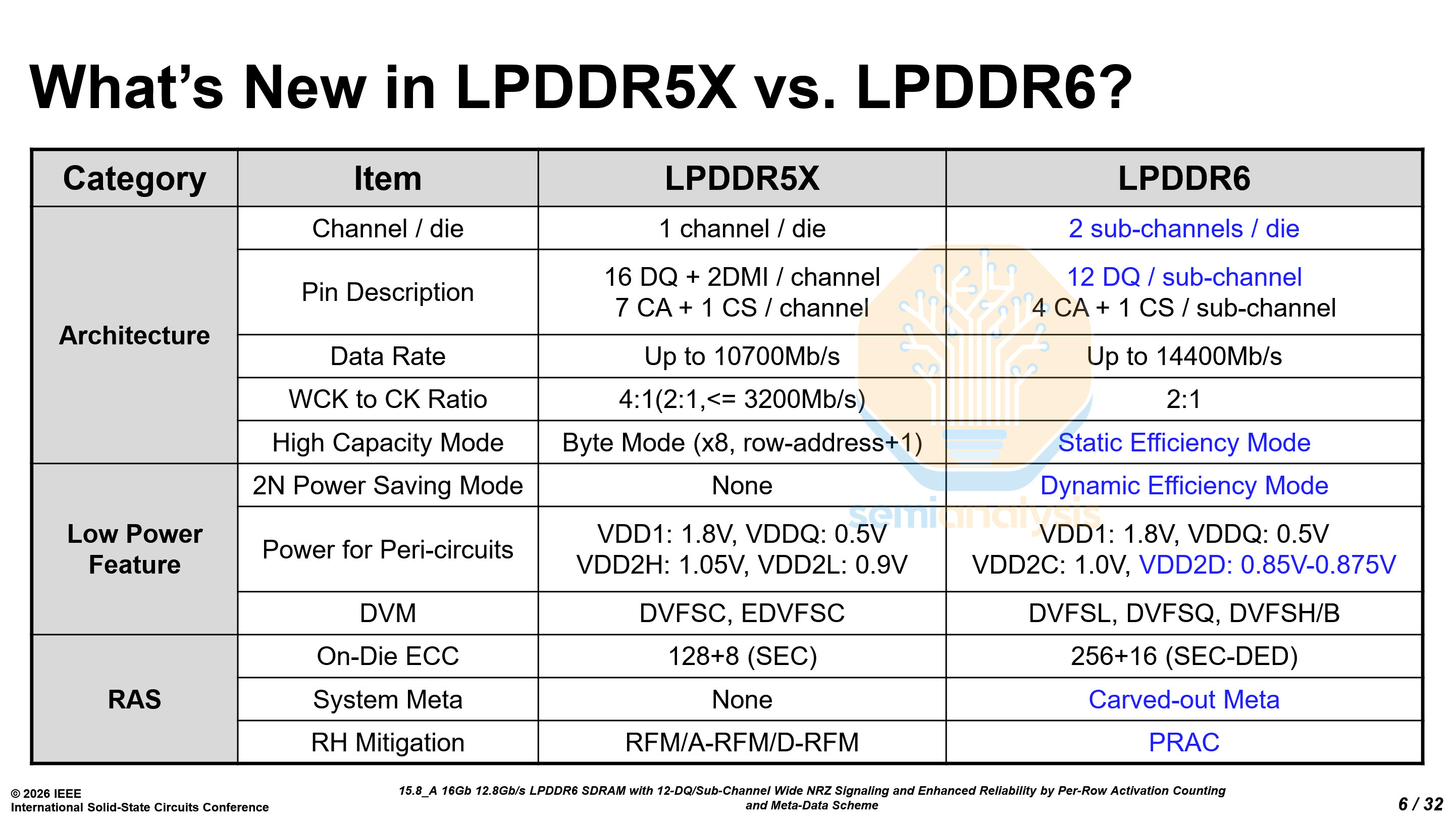
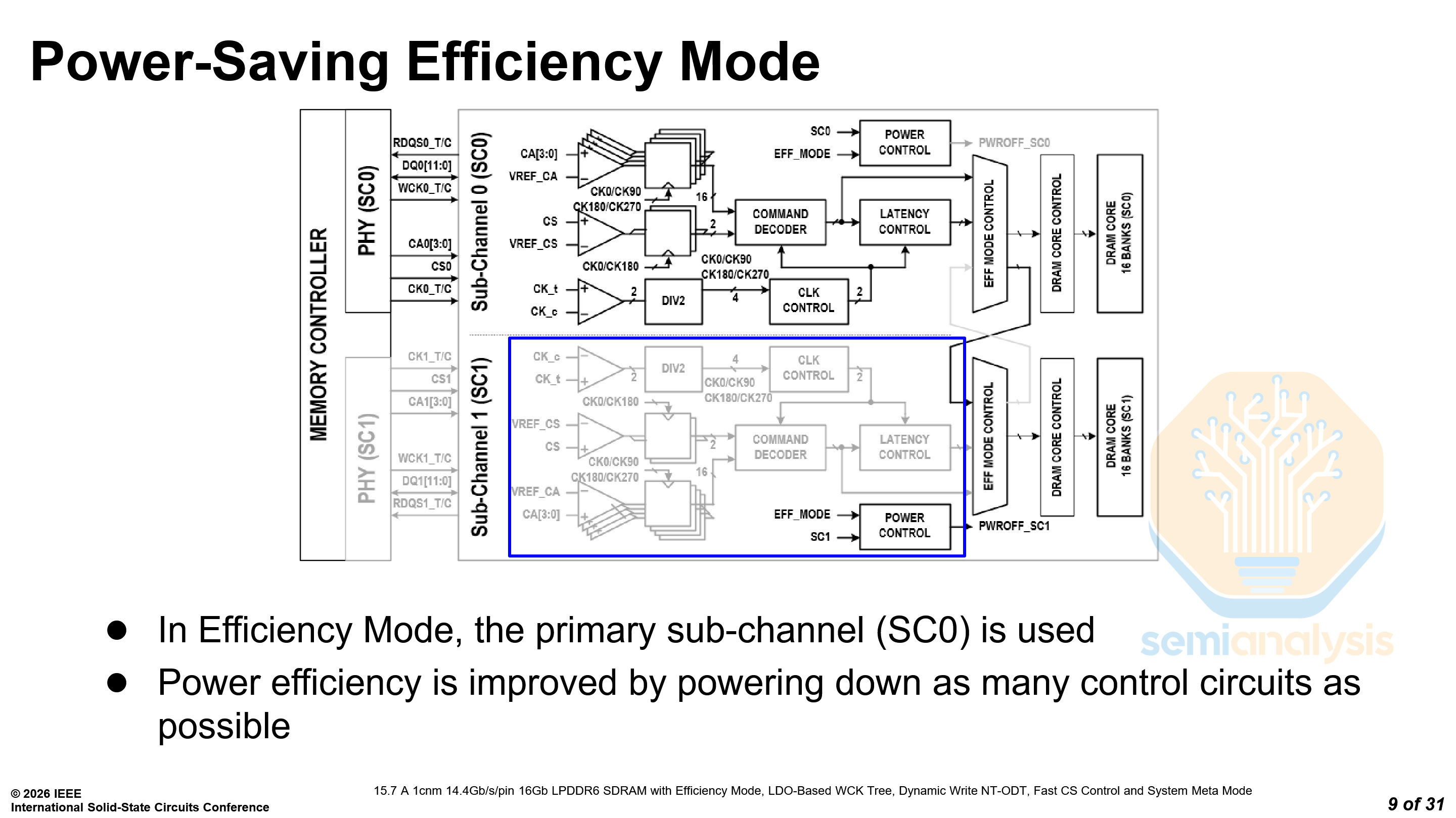
Samsung presented their LPDDR6 architecture and detailed the power-saving techniques used.
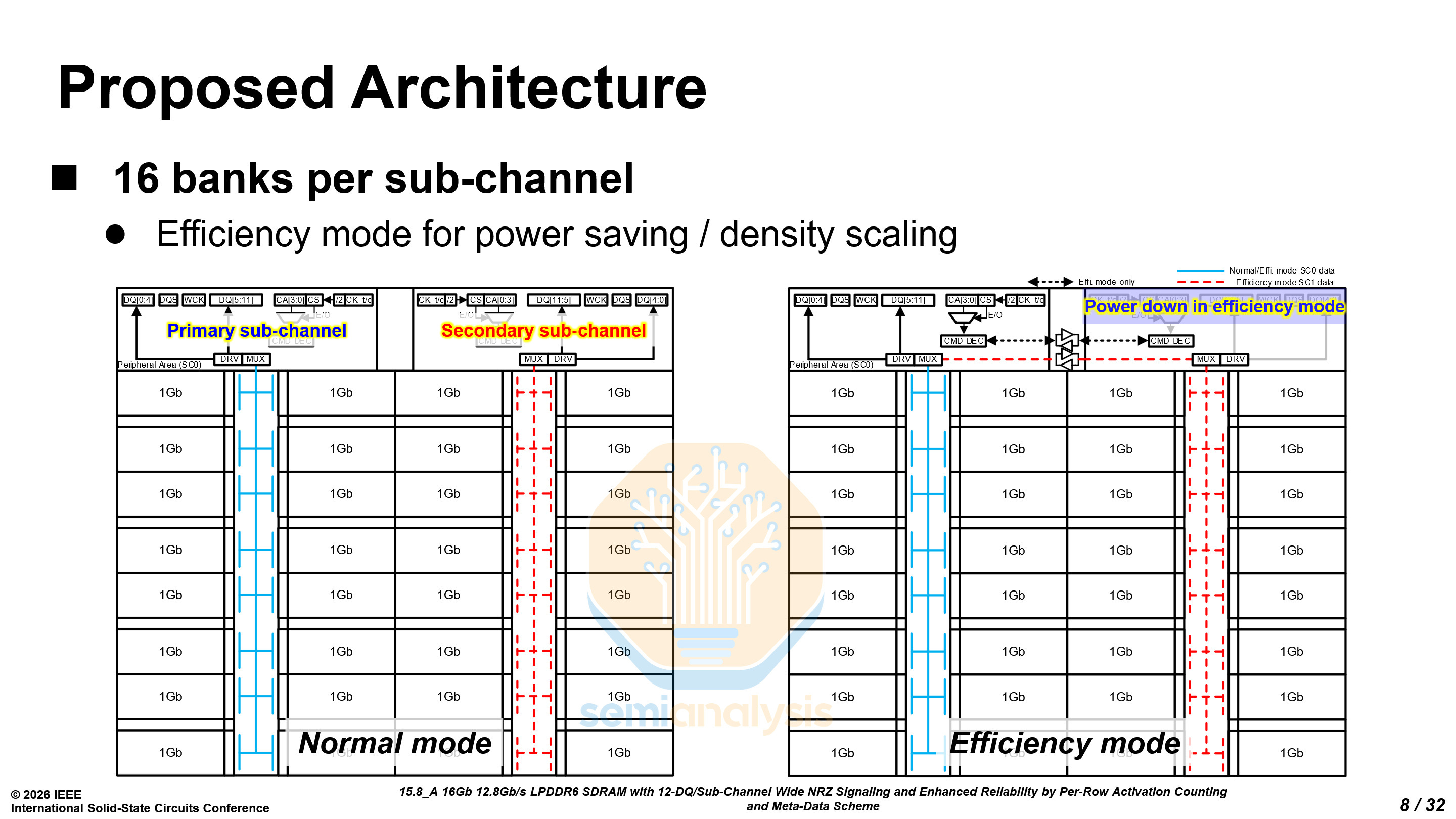
LPDDR6 adopts a 2 sub-channel per die architecture, with 16 banks in each sub-channel. It also features two modes: a normal mode and an efficiency mode. In the efficiency mode, the secondary sub-channel is powered down, and the primary sub-channel controls all 32 banks. However, there is a latency penalty for accessing data in the secondary sub-channel.
The dual sub-channel architecture also means that there is twice the amount of peripheral circuitry, such as command decoders, serialization and control. From the die shots provided by both Samsung and SK Hynix, the penalty is about 5% of the total die area, leading to a reduction in total bits per wafer.
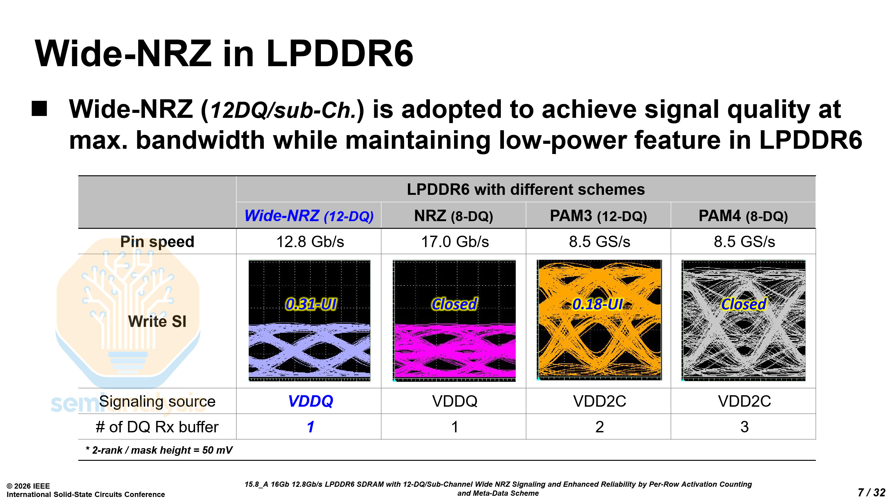
Unlike GDDR7, which uses PAM3 signaling, LPDDR6 will continue to use NRZ. However, it does not use standard NRZ as the eye would not have sufficient margin. It uses wide NRZ with 12 data (DQ) pins per sub-channel and a burst length of 24 per operation.
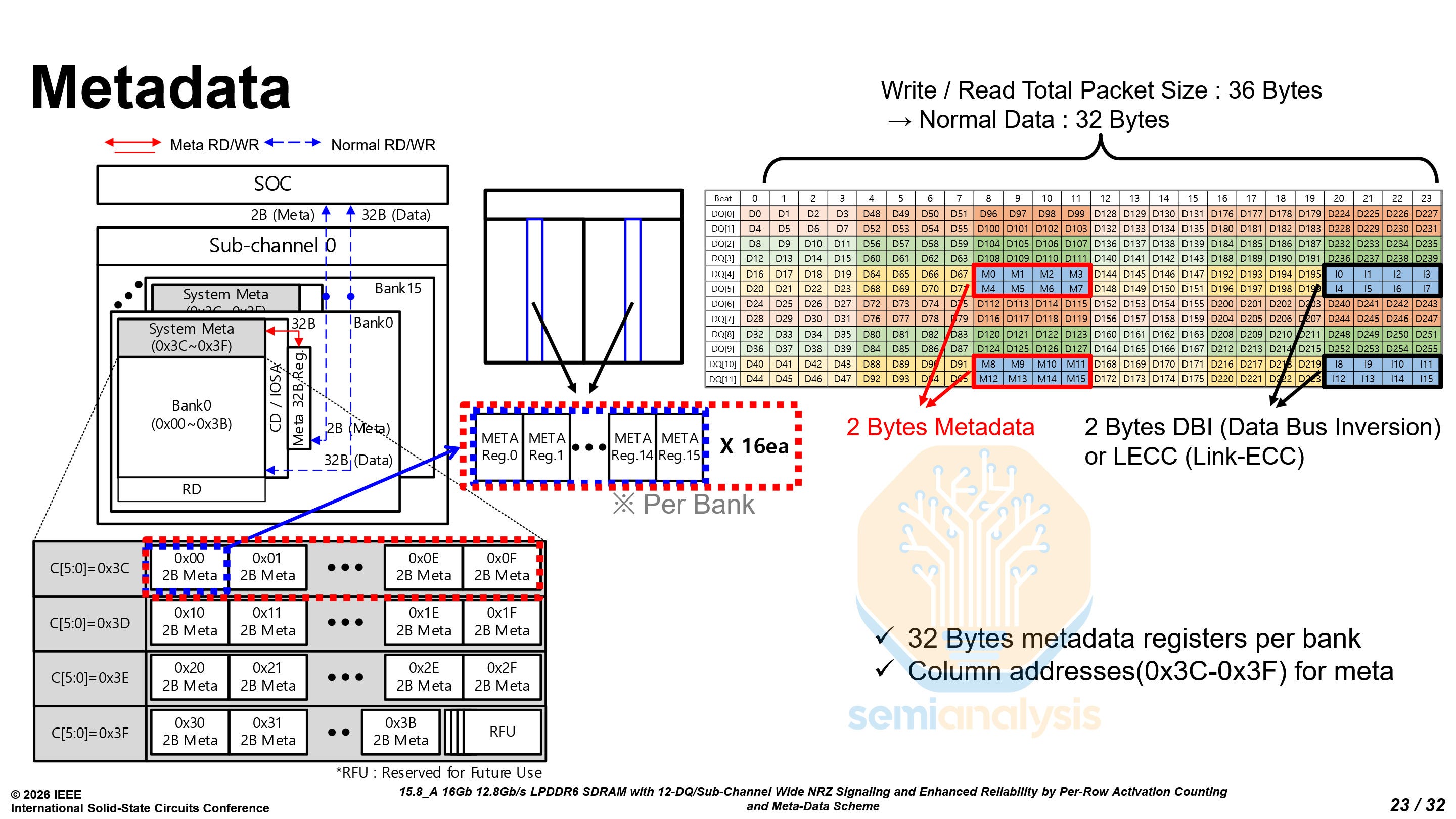
For those of you doing the math, 12×24 is 288, not a power of two. The remaining 32 bits are split into 2 use cases, 16 for metadata like ECC, and 16 for Data Bus Inversion (DBI).
DBI is a power-saving and signal integrity mechanism. Before a burst is sent out, the controller checks if more than half the bits would switch state compared to the previous burst. If so, the controller inverts all the bits and sets a DBI flag, so that the receiver knows to invert them to get the actual data. This limits the maximum number of simultaneous switching outputs to half the bus width, reducing power consumption and supply noise.
To calculate the effective bandwidth, you must account for these metadata and DBI bits like so: Bandwidth = Data Rate × Width (24 b) × Data (32 b) / Packet (36 b).
For 12.8 Gb/s, you get 34.1 GB/s, and for 14.4 Gb/s, you get 38.4 GB/s.
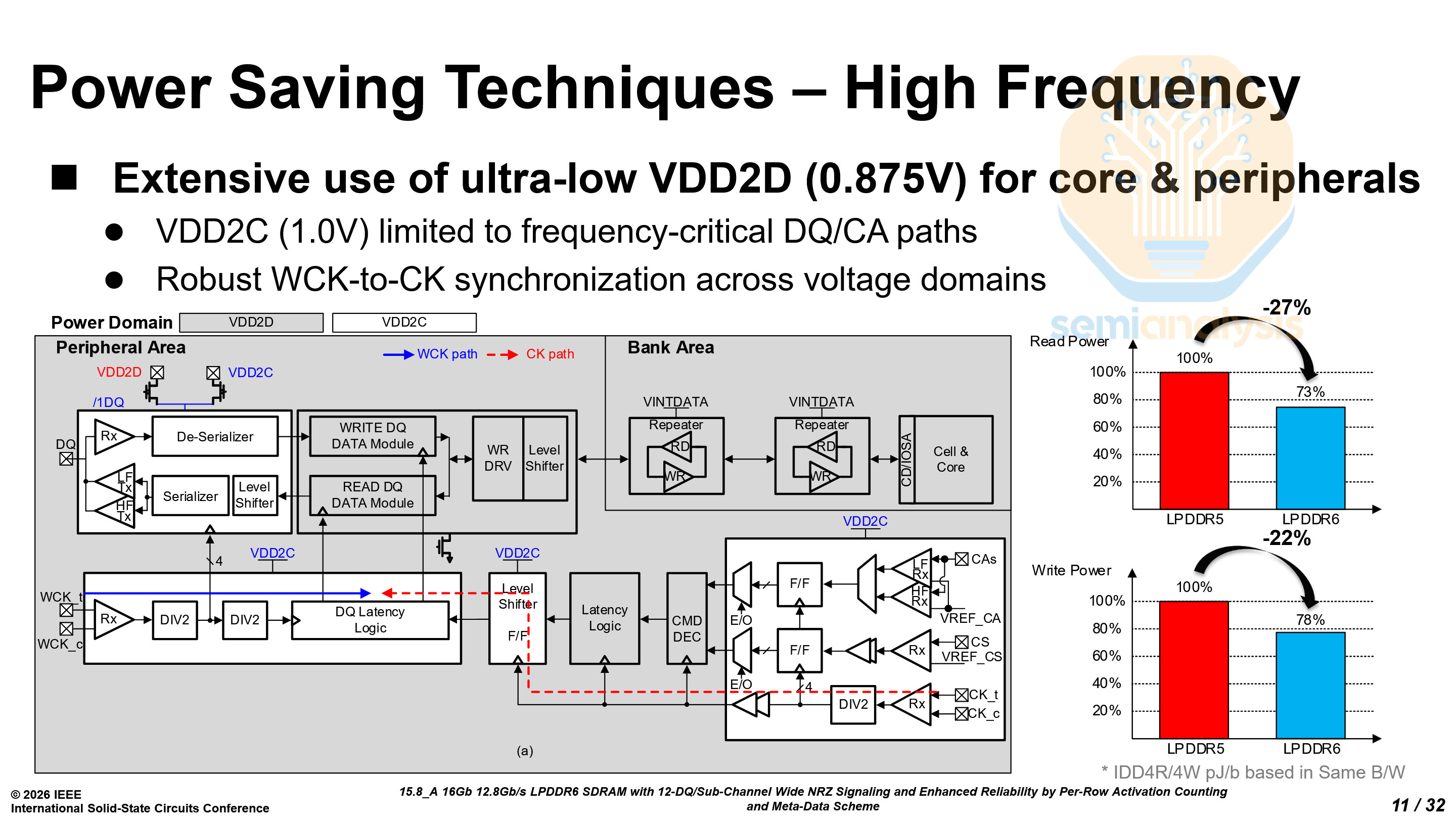
LPDDR6 has two constant power domains, VDD2C at 0.875V and VDD2D at 1.0V. By carefully choosing which peripheral logic is using which power domain, read power has been reduced by 27% and write power reduced by 22%.
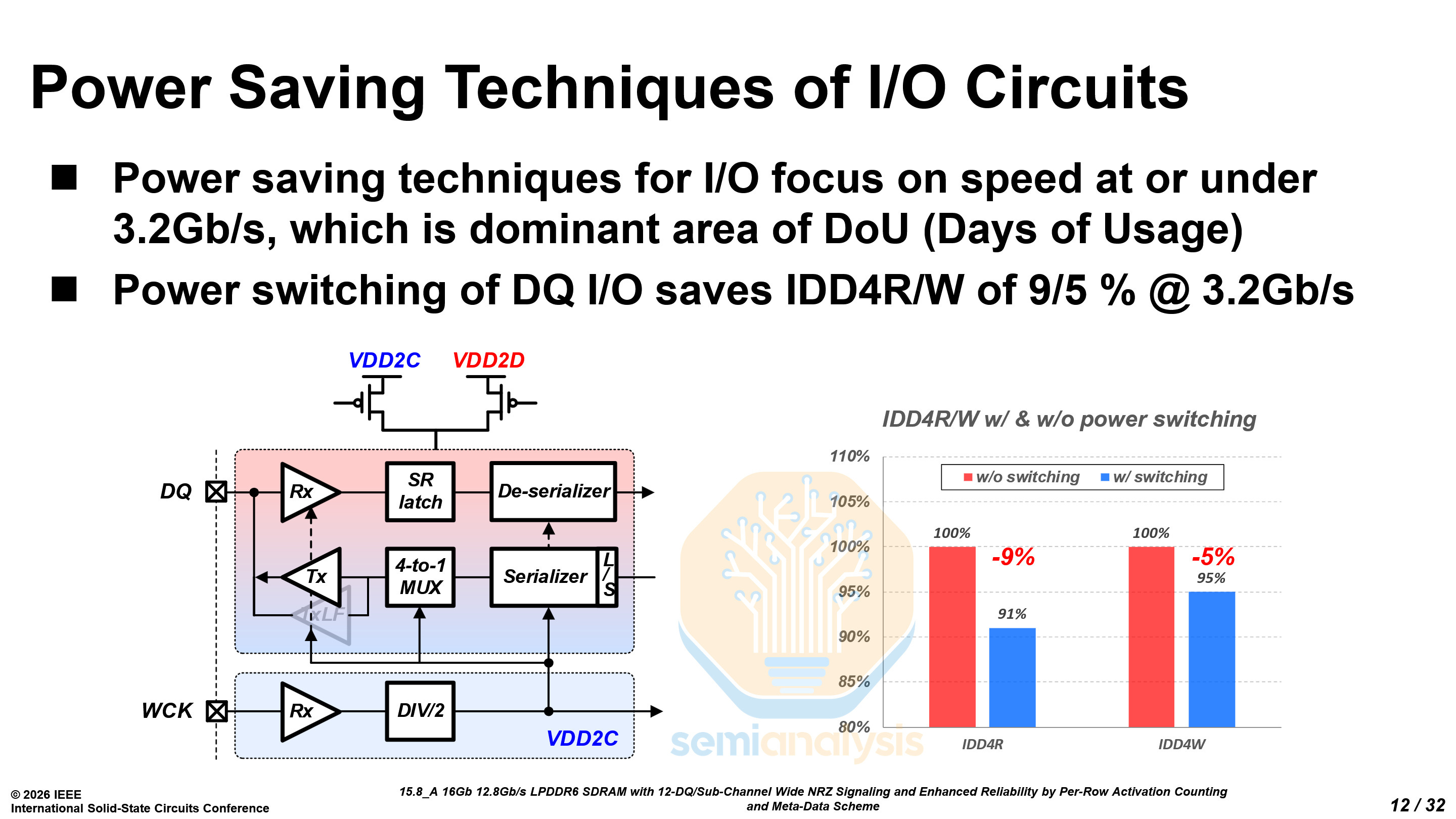
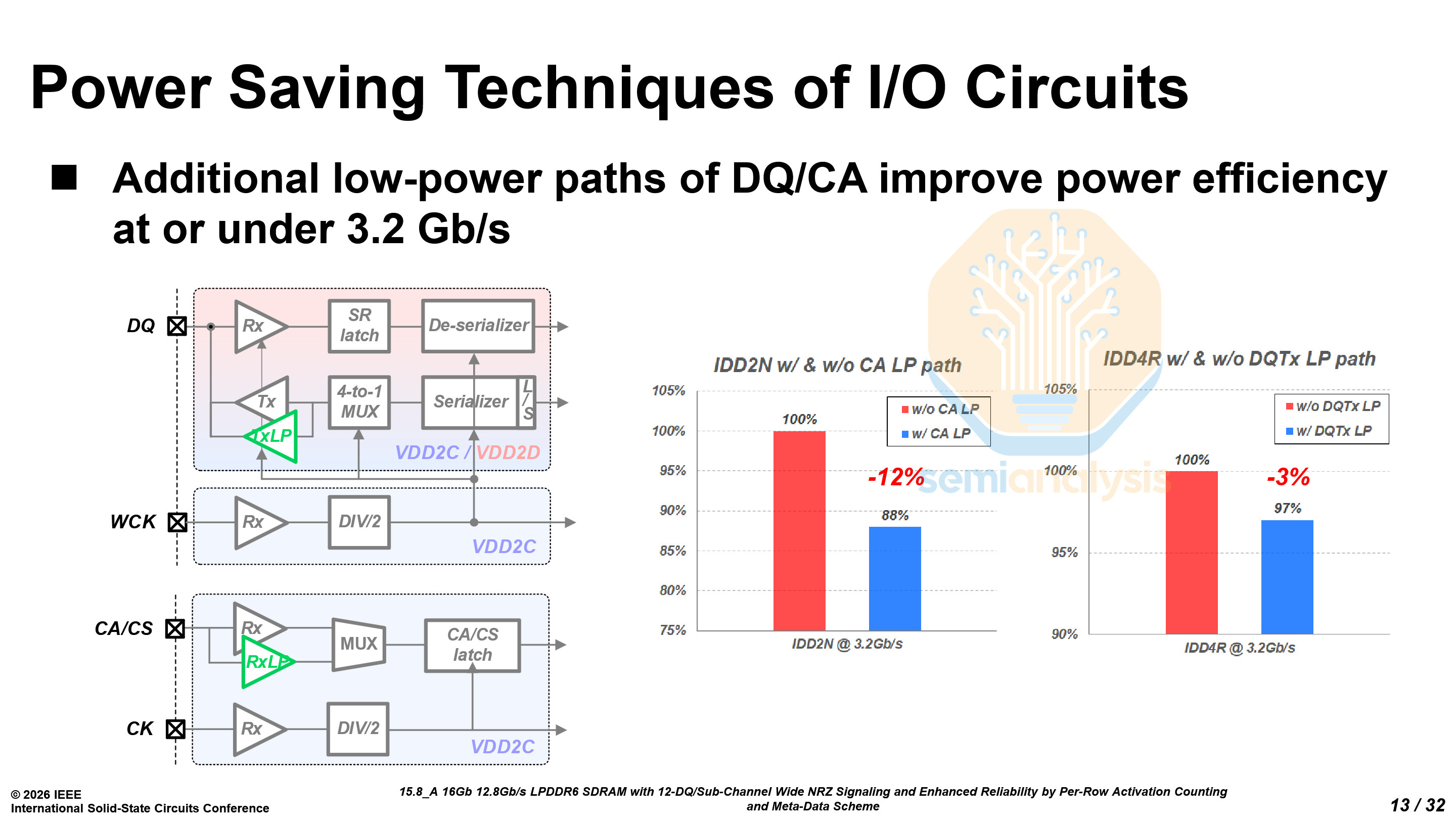
LPDDR is primarily used at low data rates of 3.2 Gb/s and below when idling. Samsung focused heavily on saving power at these lower data rates through careful use of the voltage domains, reducing both standby and read/write power consumption.
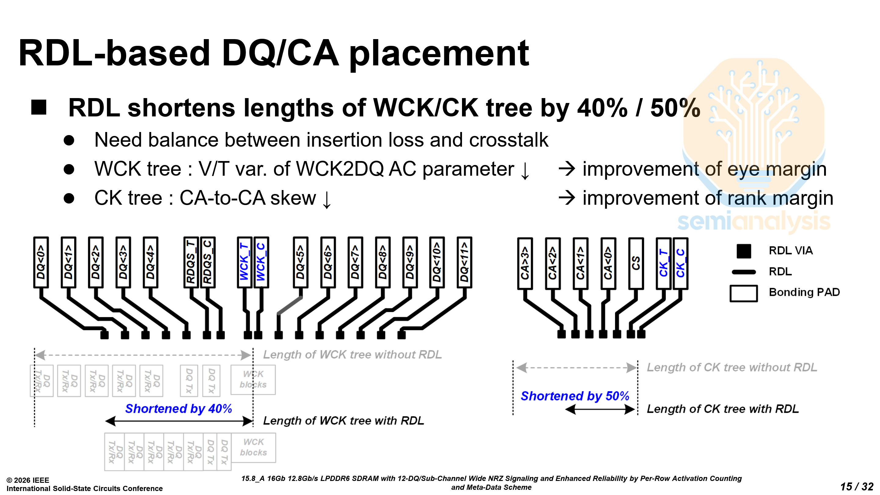
By using a redistribution layer (RDL), Samsung can locate related circuits closer together physically. This shortens critical delay paths and reduces their sensitivity to voltage and temperature variation. At the high frequencies of LPDDR6, tighter timing and reduced variation are essential.
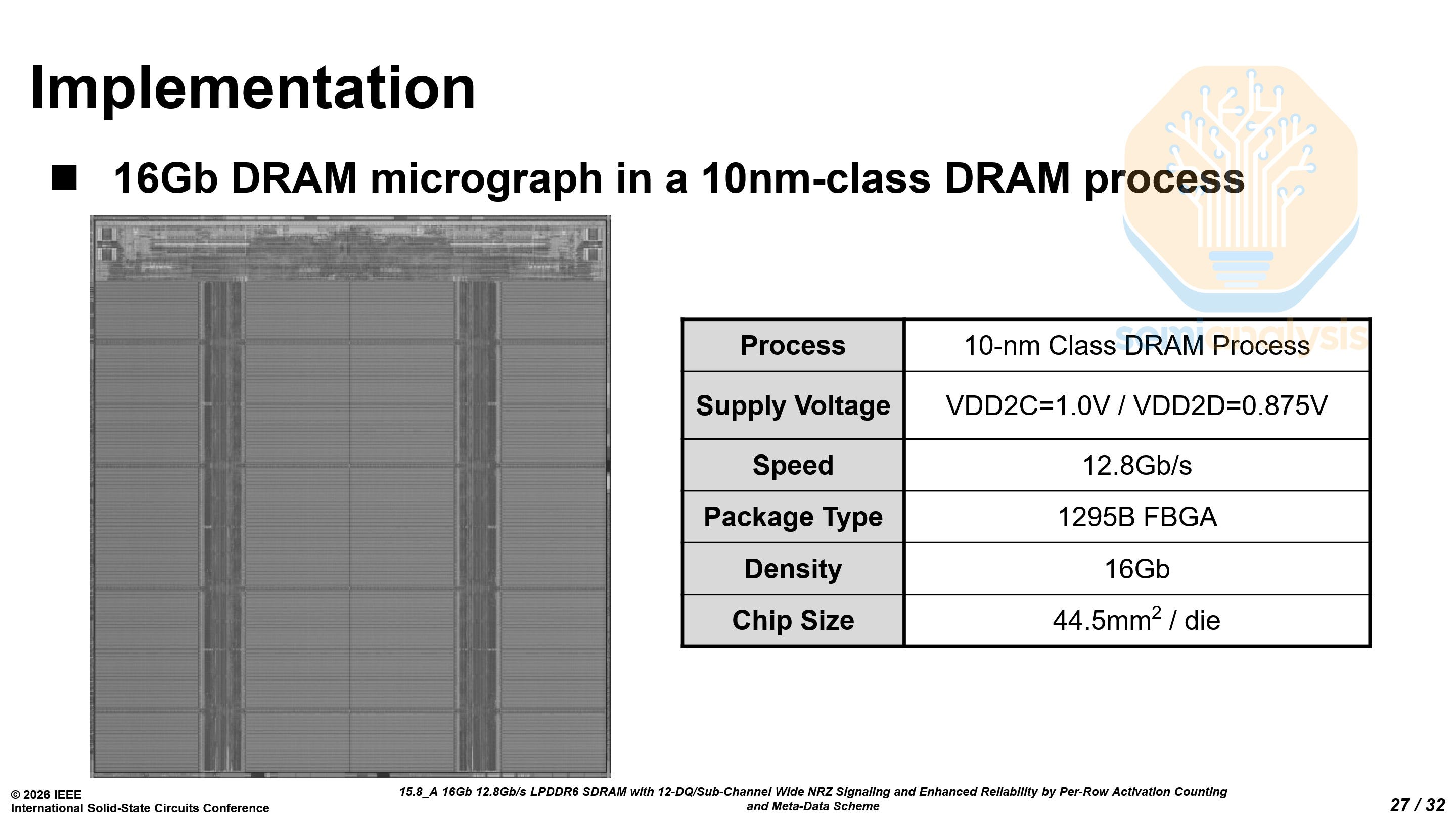
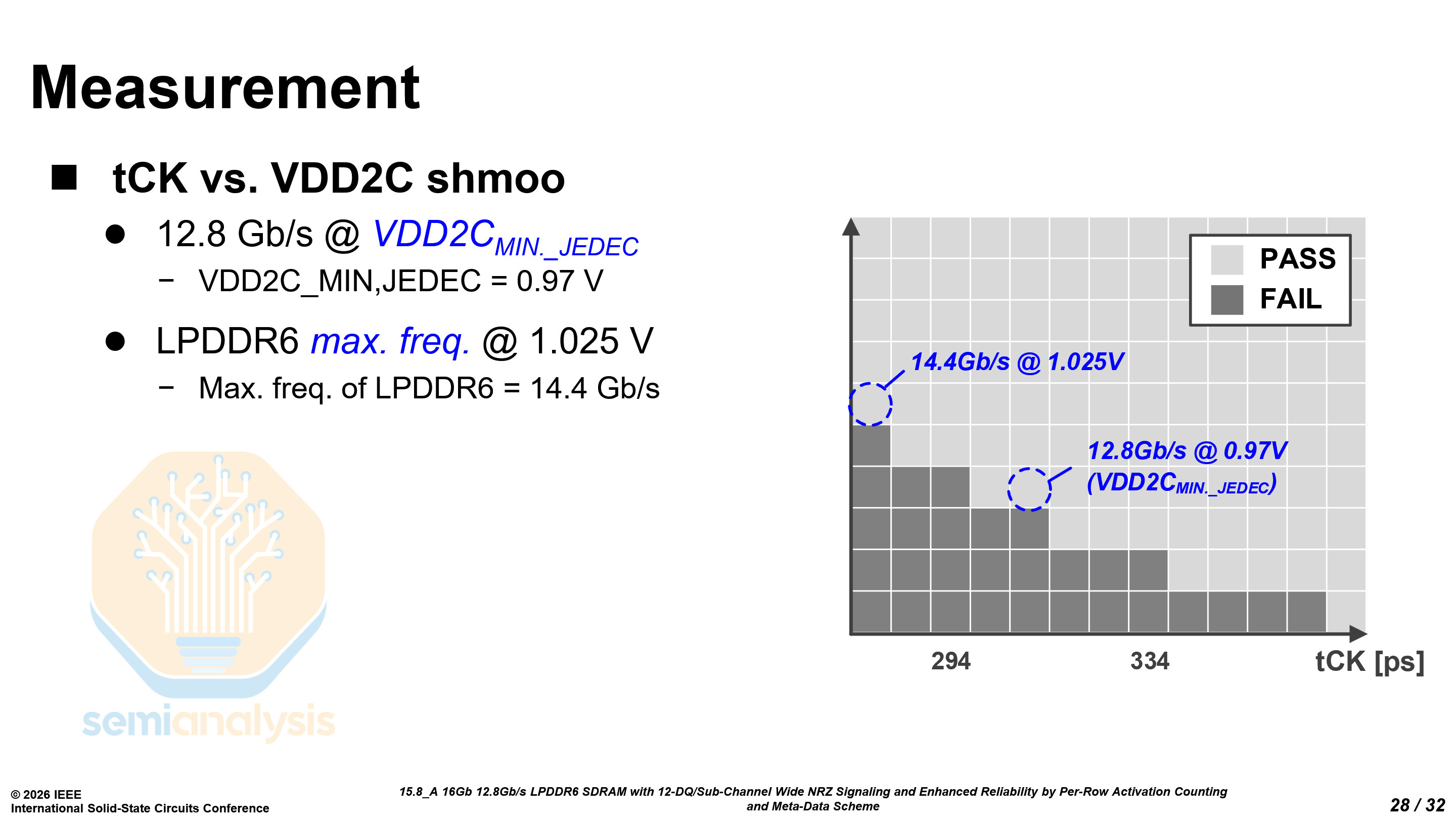
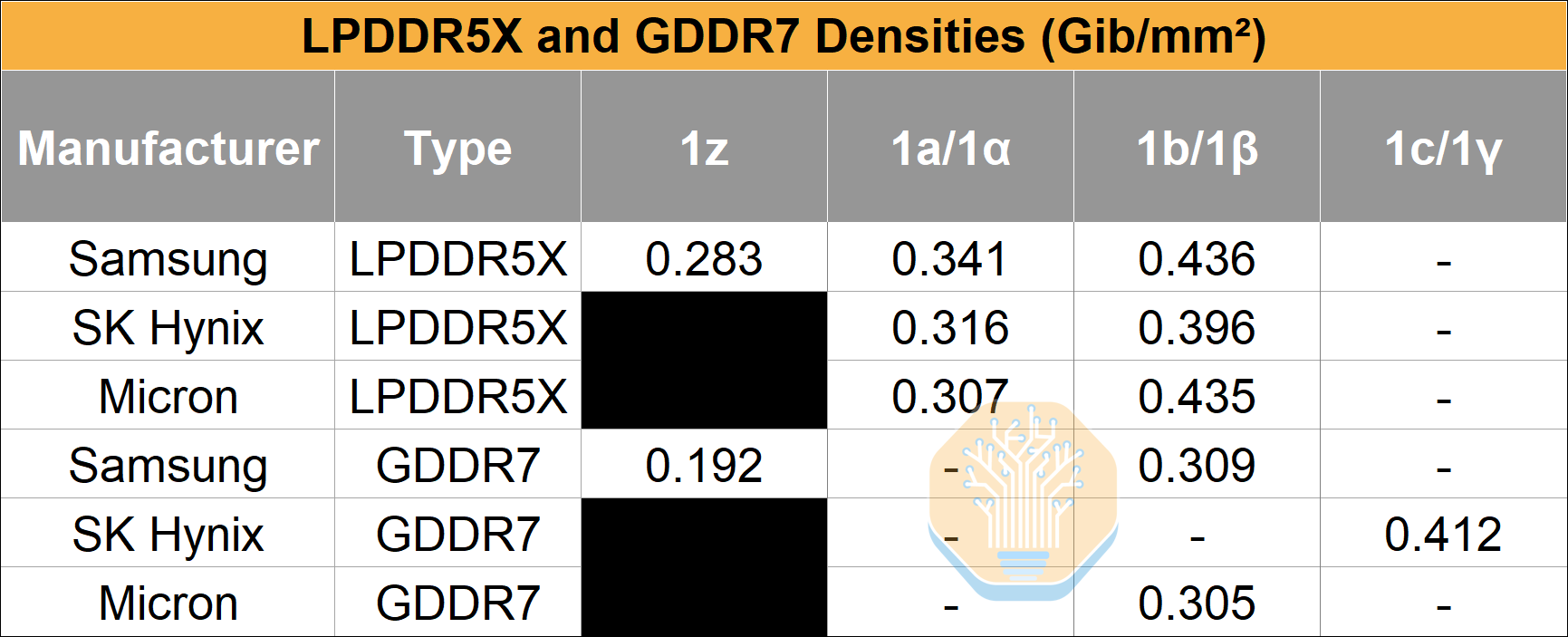
Samsung’s LPDDR6 can reach a data rate of 12.8 Gb/s at 0.97V, and up to 14.4 Gb/s at 1.025V. Each 16 Gb die is 44.5 mm², with a density of 0.360 Gb/mm² on an unknown 10nm-class process. This is considerably lower than the density of LPDDR5X on 1b at 0.447 Gb/mm² and only slightly higher than the density of LPDDR5X on 1a at 0.341 Gb/mm². While the area penalty from the dual sub-channel architecture does partially contribute, there seem to be other problems with the LPDDR6 as well. The memory density described leads us to believe that this prototype LPDDR6 chip was manufactured on their 1b process.
Samsung SF2 LPDDR6 PHY - Paper 37.3
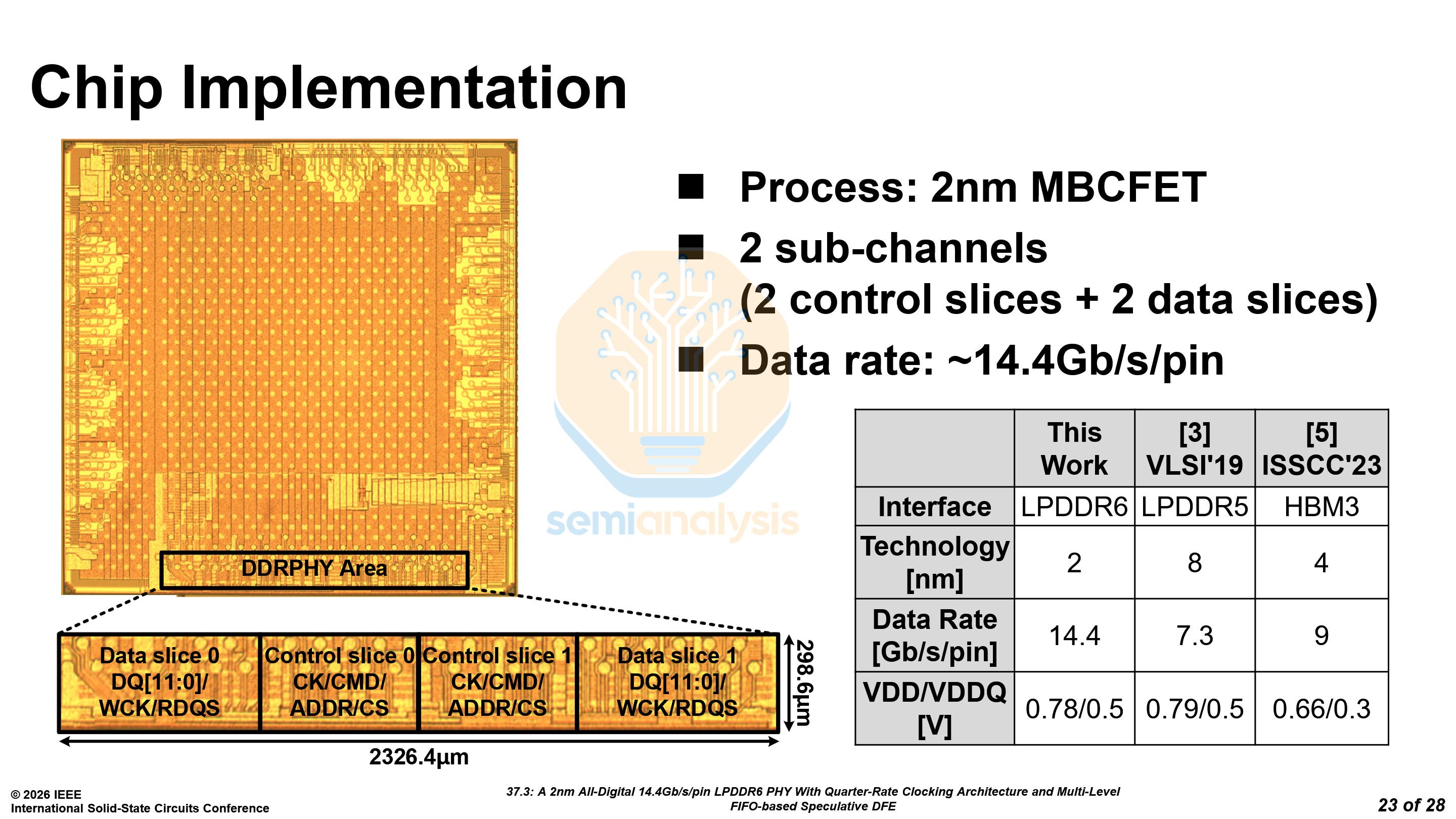
Samsung also unveiled PHYs on the logic die interface with LPDDR6. The PHYs are fabricated on their new SF2 process and support up to 14.4 Gb/s. The PHYs take up 2.32 mm of shoreline and 0.695 mm² of area, with bandwidth densities of 16.6 Gb/s/mm and 55.3 Gb/s/mm² respectively.
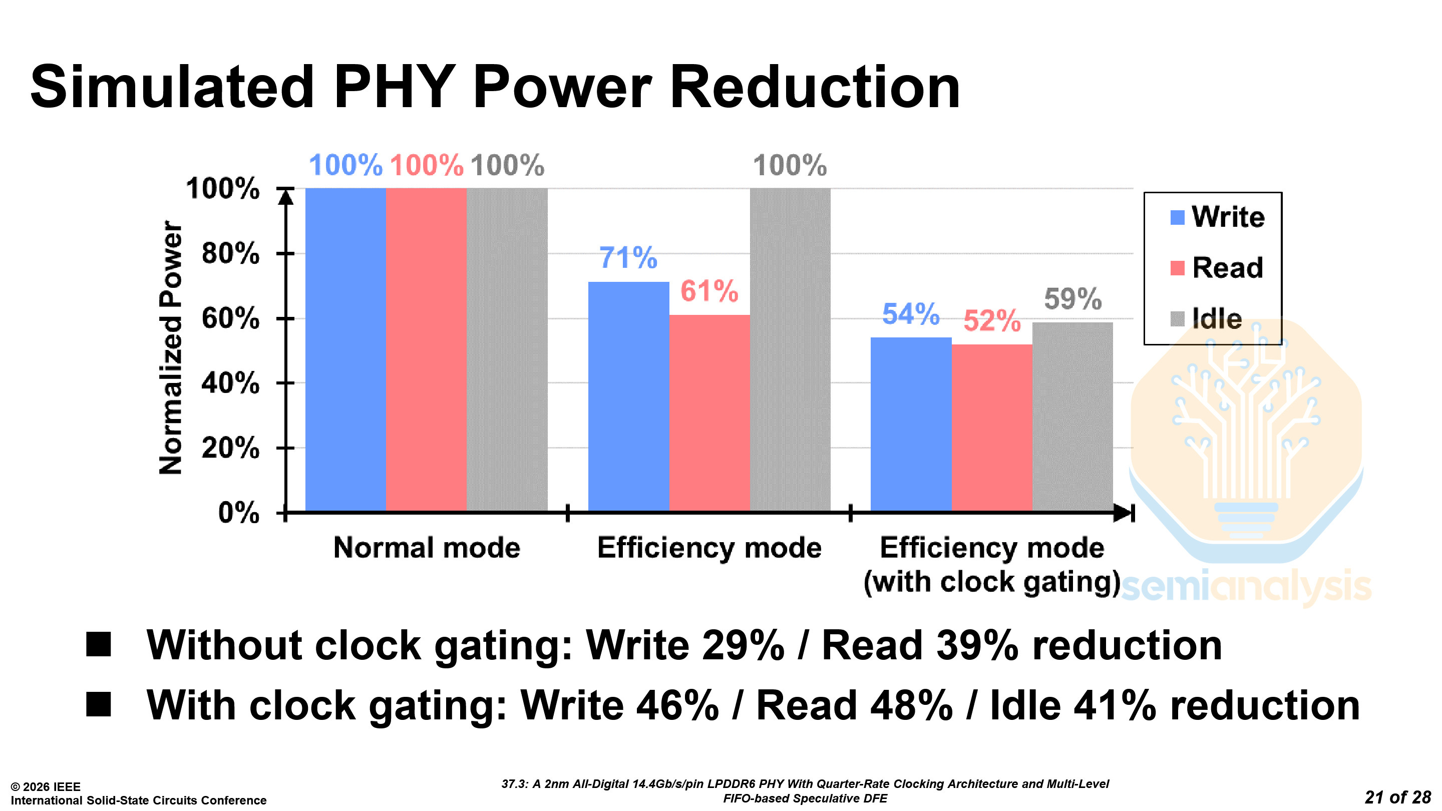
The PHYs also support the efficiency mode implemented by the LPDDR6 chips, which can reduce read power by 39% and write power by 29%.
The PHYs can augment the efficiency mode by gating the high-speed clock path for the inactive secondary sub-channel. With clock-gating, the power reduction reaches almost 50% for reading and writing, and idle power is reduced by 41%.
SK Hynix 1c LPDDR6 - Paper 15.7
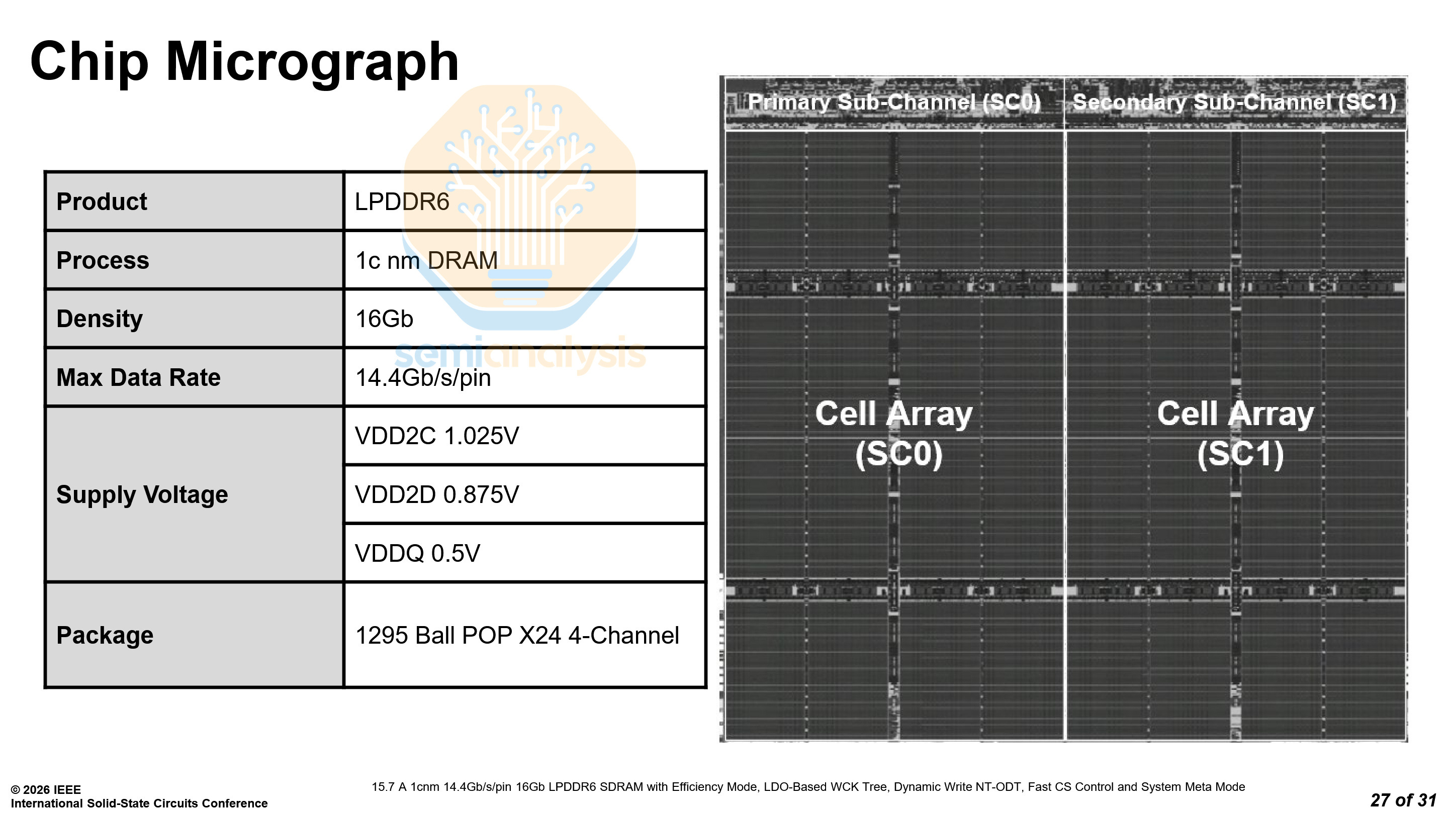
SK Hynix unveiled their first 1c DRAM products, both in LPDDR6 and in GDDR7 packages. Their LPDDR6 can operate at a data rate of up to 14.4 Gb/s, 35% faster than the fastest LPDDR5X, and at lower power.
Although SK Hynix did not state the area or density of the LPDDR6 chip, we estimate the bit density will reach 0.59 Gb/mm², based on the relative density increase of their GDDR7.
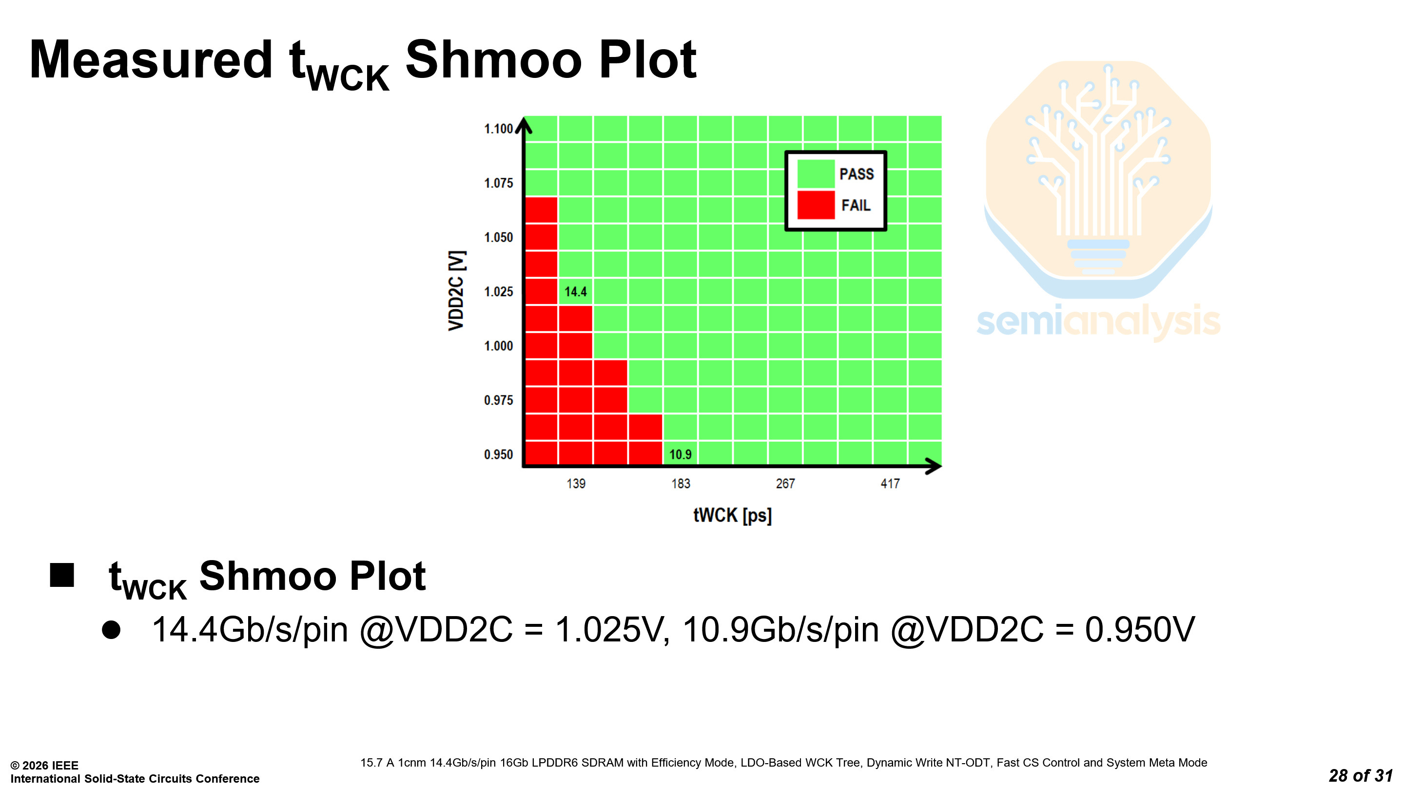
In their shmoo plot, SK Hynix showed that they can reach a data rate of 14.4 Gb/s at 1.025V, the same as Samsung. However, they can only reach 10.9 Gb/s at 0.95V as compared to Samsung’s 12.8 Gb/s at 0.97V. This indicates that SK Hynix may have worse power efficiency at lower pin speeds when compared to Samsung, having to run at higher voltages to maintain reliability.
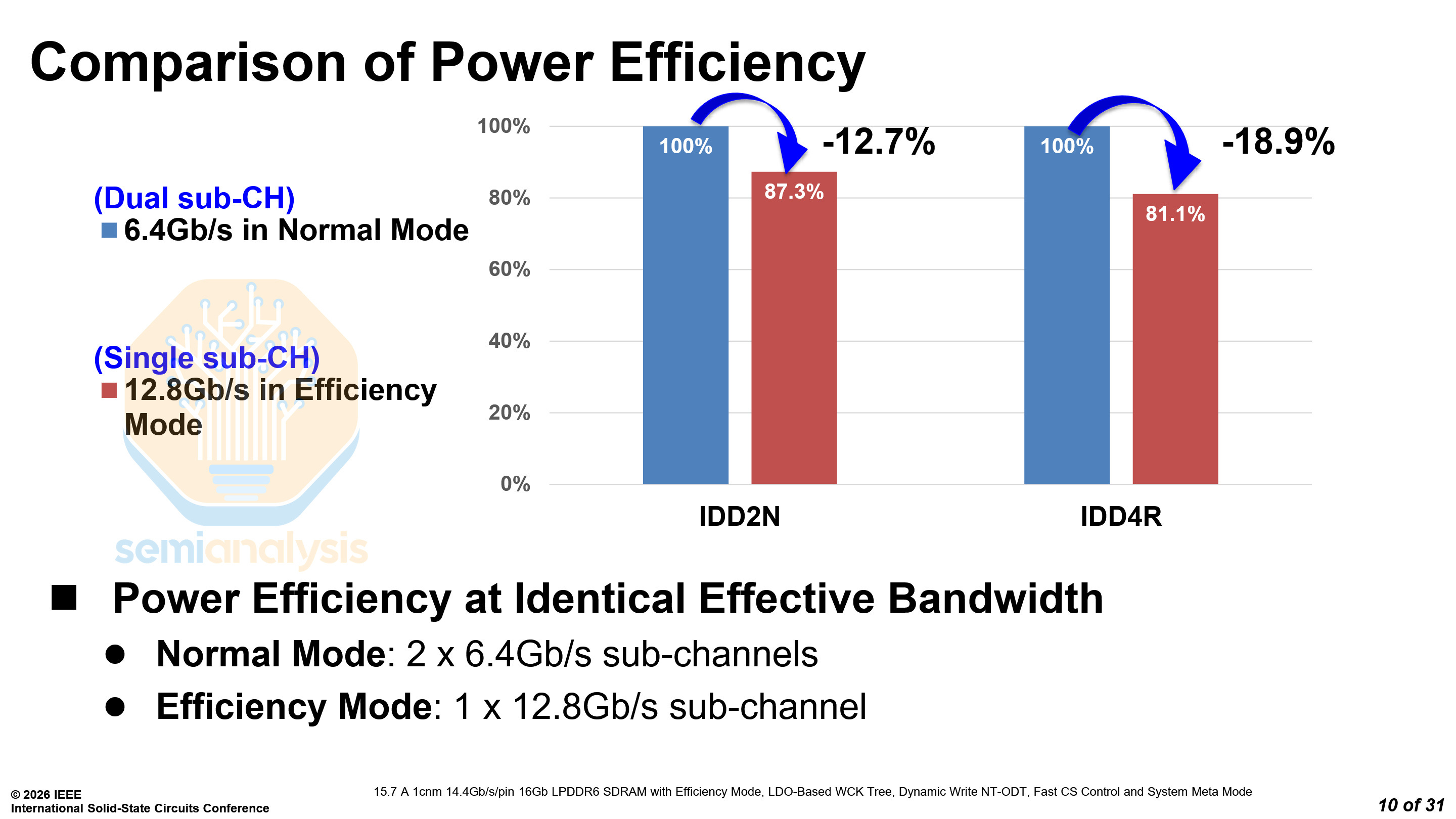
Like Samsung’s LPDDR6, SK Hynix’s LPDDR6 also features two modes, a normal mode and an efficiency mode. The efficiency mode runs at 12.8 Gb/s over a single sub-channel, with 12.7% and 18.9% lower standby and operational current draw respectively compared to normal mode.
SK Hynix 1c GDDR7 - Paper 15.9
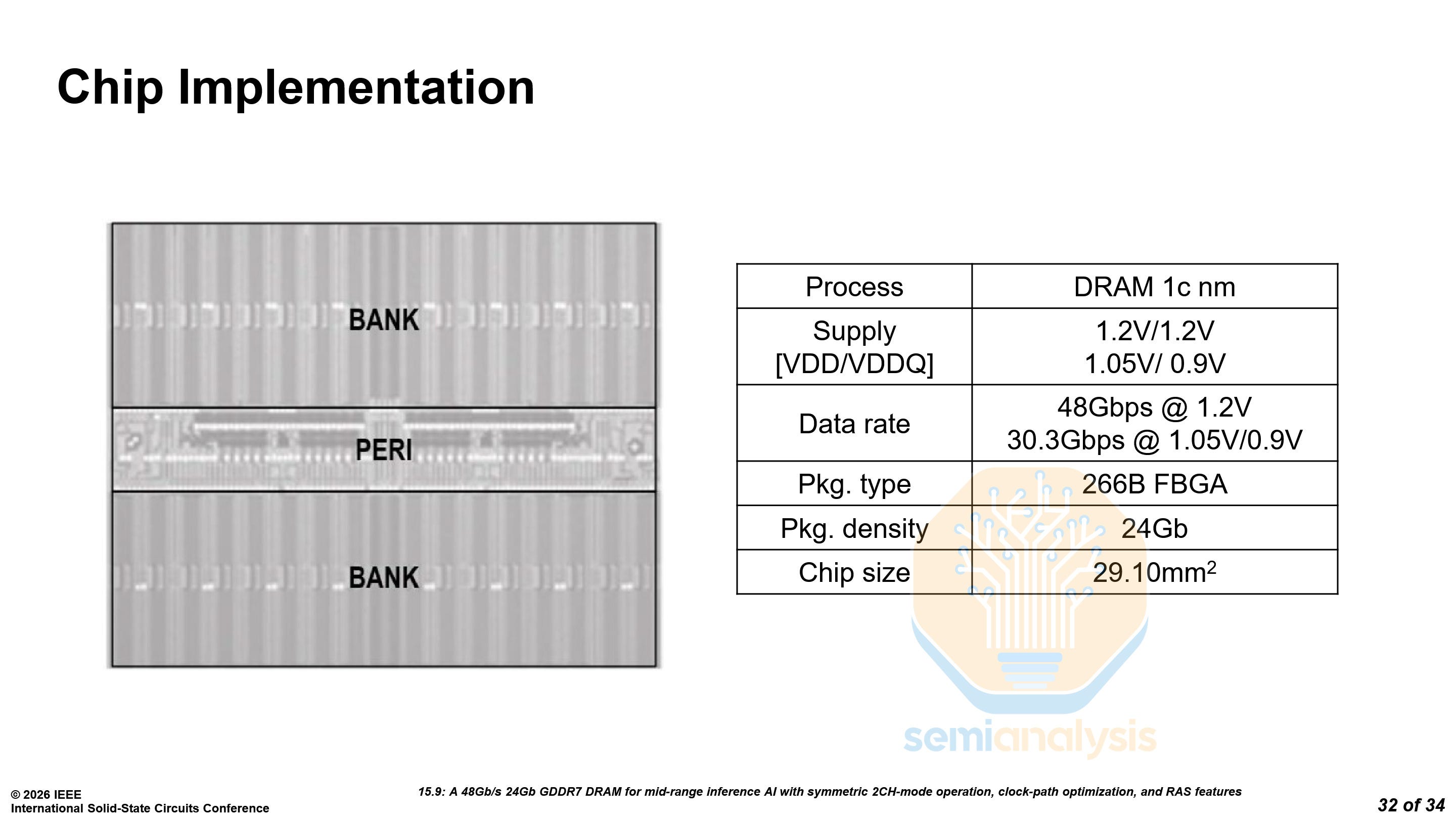
While the LPDDR6 is a generational leap with new memory technology, SK Hynix’s GDDR7 on their 1c process shows an even greater improvement, clocking up to 48 Gb/s at 1.2V/1.2V. Even at only 1.05V/0.9V, it can clock up to 30.3 Gb/s, higher than the 30 Gb/s memory in the RTX 5080.
The bit density achieved is 0.412 Gb/mm², compared to 0.309 Gb/mm² on Samsung’s 1b process, and 0.192 Gb/mm² on Samsung’s older 1z process.
GDDR7 has lower bit density than LPDDR5X, usually around 70% of the latter. Although it has much higher data rates, this comes at a cost, both in terms of power and area.
GDDR7’s lower density is a result of the significantly higher periphery area for high access speeds. The actual memory arrays thus make up a smaller percentage of die area. This more complex logic control circuit is required for the PAM3 and QDR (4 symbols per clock cycle) signaling used in GDDR7.
GDDR7 is mainly used in gaming GPU applications that require high memory bandwidth at lower cost and capacity compared to HBM. NVIDIA had announced the Rubin CPX large-context AI processor in 2025 with 128GB of GDDR7, but this has all but vanished from the 2026 roadmaps as NVIDIA focuses on rolling out their Groq LPX solutions instead.
Samsung 4F² COP DRAM - Paper 15.10
We have extensively covered challenges in continuing to scale DRAM.

At VLSI 2025, SK Hynix detailed their own 4F² Peri-Under-Cell (PUC) DRAM. At ISSCC, Samsung disclosed their own implementation of a 4F² Cell-on-Peripheral (COP) DRAM. PUC and COP are the same architecture with different names.
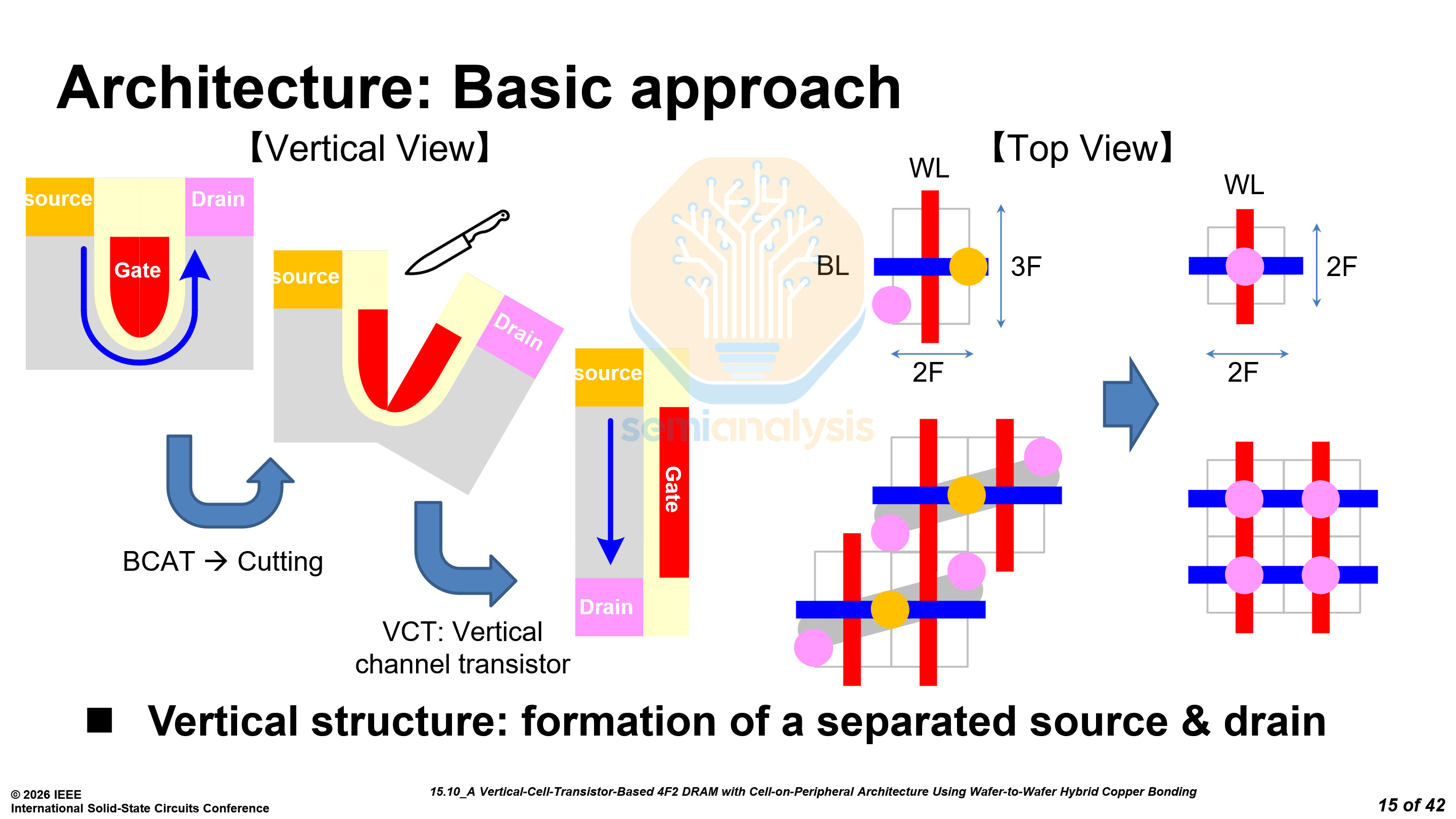
The architecture for 4F² cells is the same as SK Hynix’s, with vertical channel transistors (VCT), and capacitors above the drain.
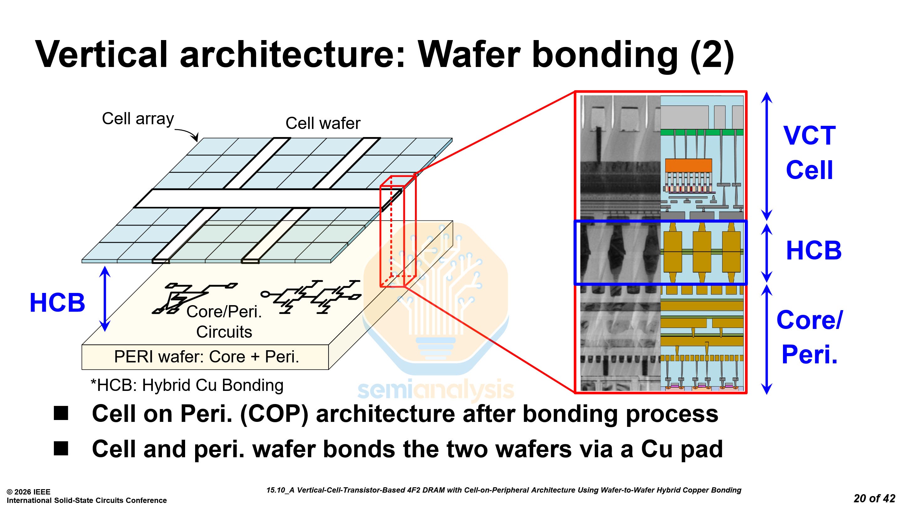
The vertical architecture presented by Samsung is essentially the same as that used by SK Hynix, with a cell wafer hybrid bonded on top of a peripheral wafer. With this architecture, it is possible to use a DRAM node for the cell wafer while using a more advanced logic node for the periphery.
Samsung notes that hybrid bonding for COP has already been used for NAND. This is true for other NAND manufacturers, but Samsung has not brought hybrid bonding for NAND into high volume production and is still years away from doing so.
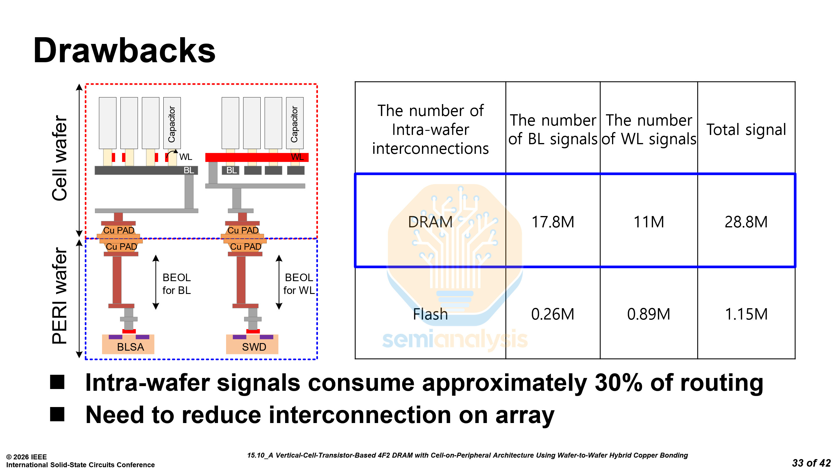
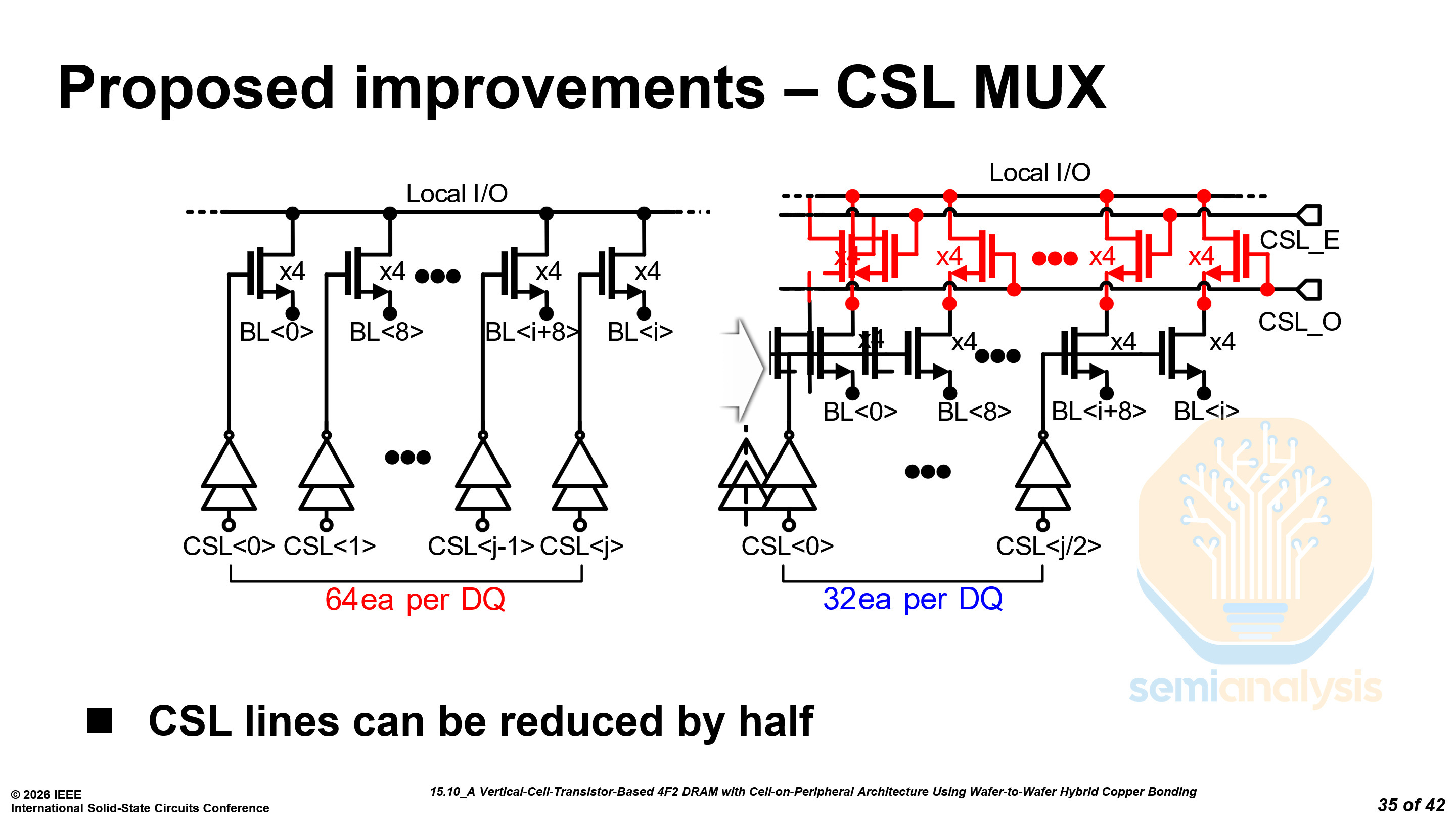
Moreover, the number of inter-wafer connections for DRAM is an order of magnitude higher than for NAND and requires much tighter pitches. To reduce the number of inter-wafer interconnections, Samsung has employed two novel approaches.
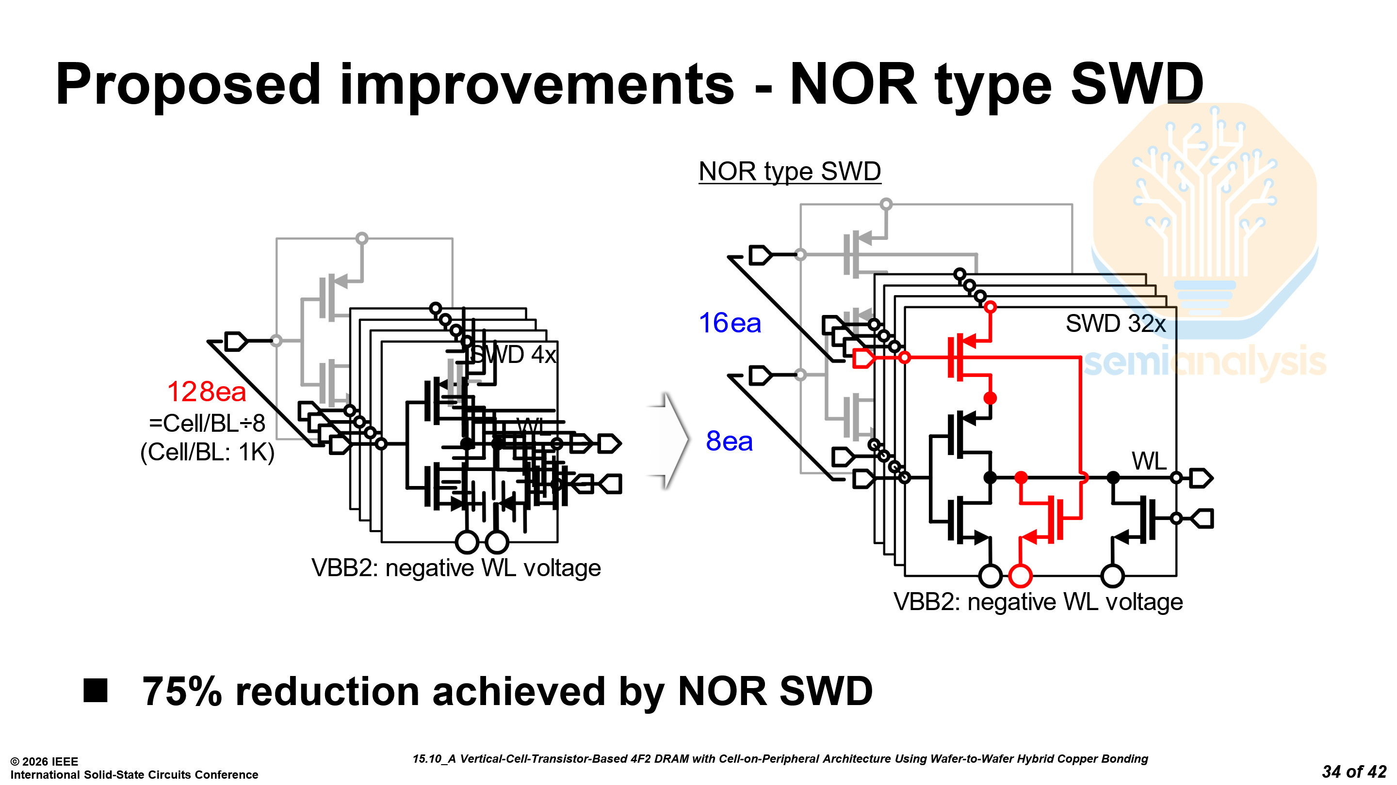
First, they have reorganized the sub-wordline drivers (SWD) from 128 per cell block to 16 groups of 8. This reduces the number of signals required for the SWD by 75%.
Next, they split the column select into an even and an odd path. This requires twice the multiplexers (MUX) but halves the column select line (CSL) count to 32 per data pin.
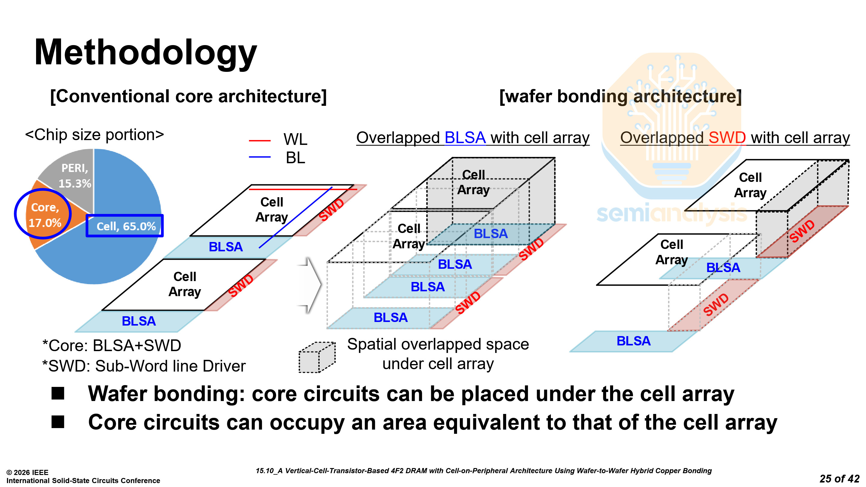
With hybrid bonding, the core circuitry, that is, bitline sense amplifiers (BLSA) and SWD can be placed under the cell array. The goal is for the core circuits to occupy the same area as the cell array to increase overall density.
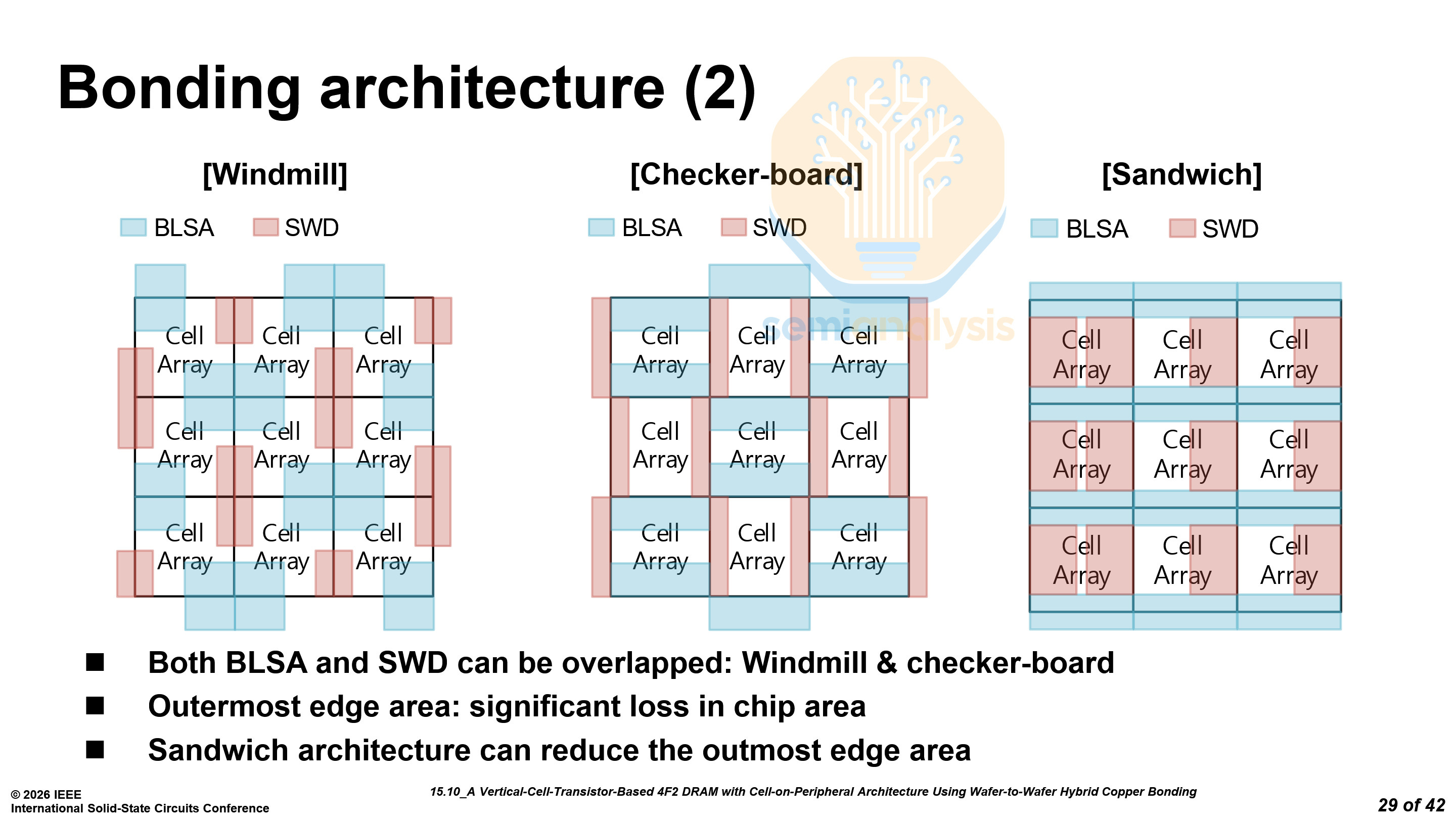
Samsung adopted the “sandwich” structure, which allows them to maximize the area efficiency of the core circuitry, and reduce the edge region area, which is not under any cells.
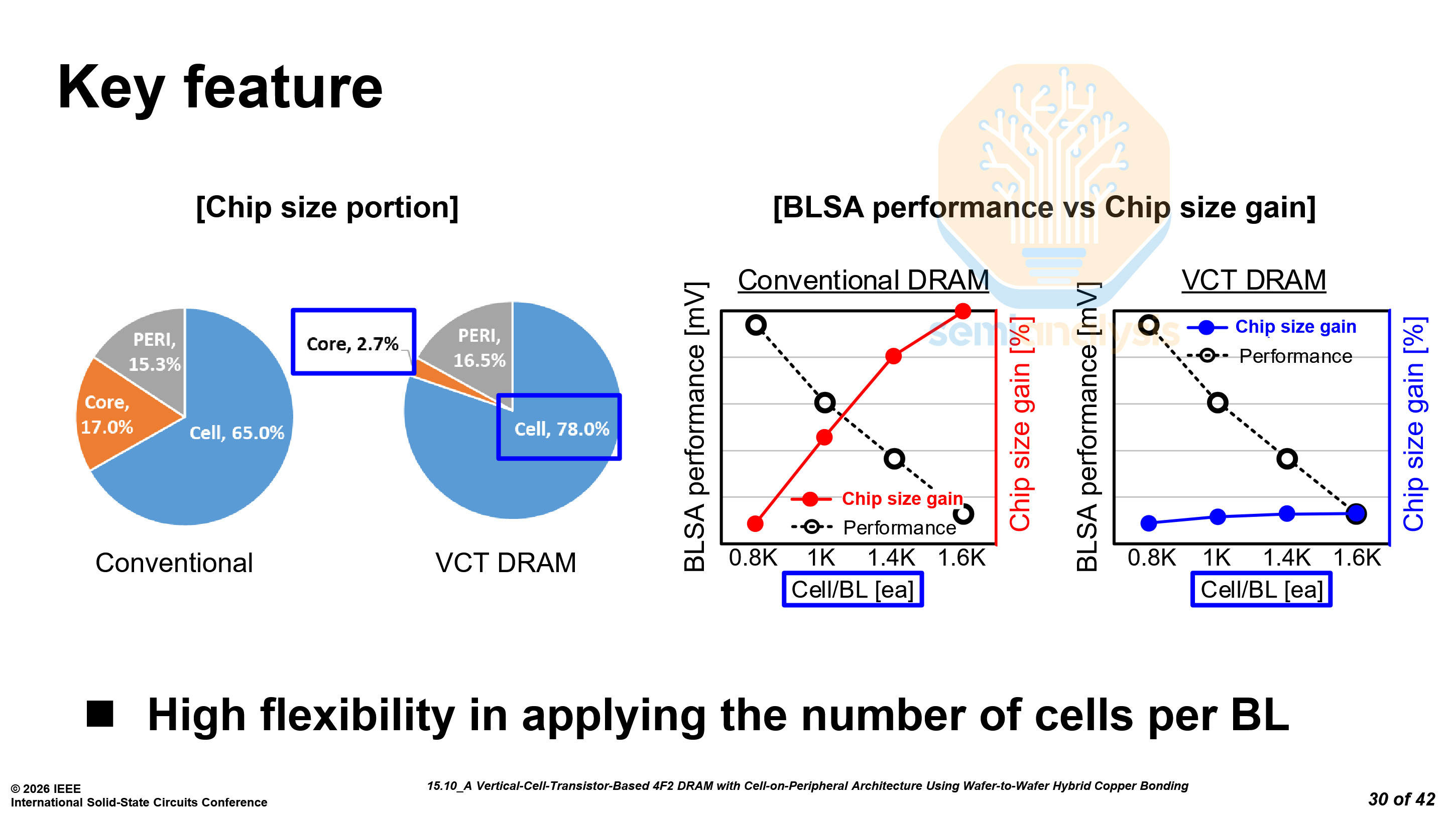
The area used by the core circuitry was reduced from 17.0% down to only 2.7%, a significant improvement, directly translating to overall die size reductions.
In traditional DRAM, increasing the number of cells per bitline would result in a significant increase in chip area, while for VCT DRAM, the increase is almost negligible as the core circuitry is all below the cells.
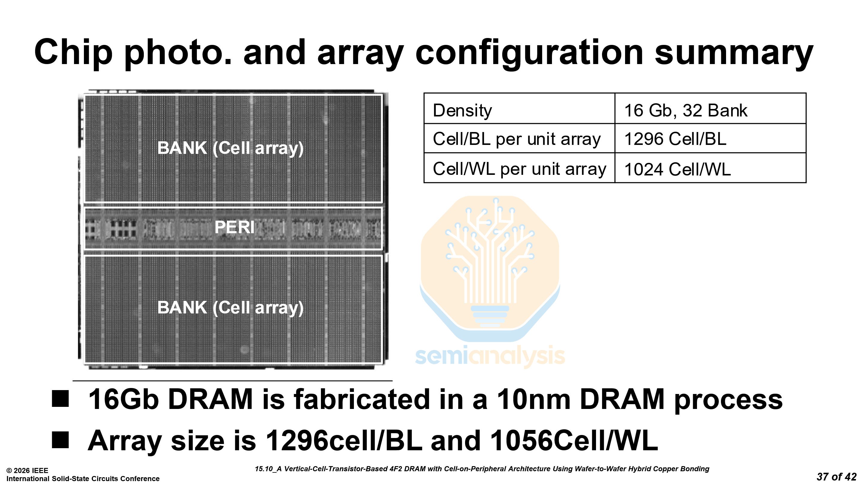
Samsung did not provide any density figures for this chip, only stating that it was a 16 Gb chip on a 10nm DRAM process.
Samsung noted that the VCT DRAM suffers from the floating-body effect, increasing leakage and reducing retention time. Mitigating this effect remains a key challenge for 4F² adoption.
Despite these challenges, we still expect 4F² hybrid bonded DRAM to arrive in the latter part of the decade as early as the generation after 1d. Our memory model tracks the timing and ramp of each node in detail. The current memory pricing landscape largely incentivizes the ramp and introduction of new nodes with higher bit densities to improve bit output per fab. On the otherhand, performance/$ of memory is highly sought after more than capacity for many use cases.
SanDisk/Kioxia BiCS10 NAND - Paper 15.1
SanDisk and Kioxia demonstrated their BiCS10 NAND, with 332 layers and 3 decks. This is the highest reported NAND bit density, at 37.6 Gb/mm², dethroning the previous champion, SK Hynix’s 321L V9.
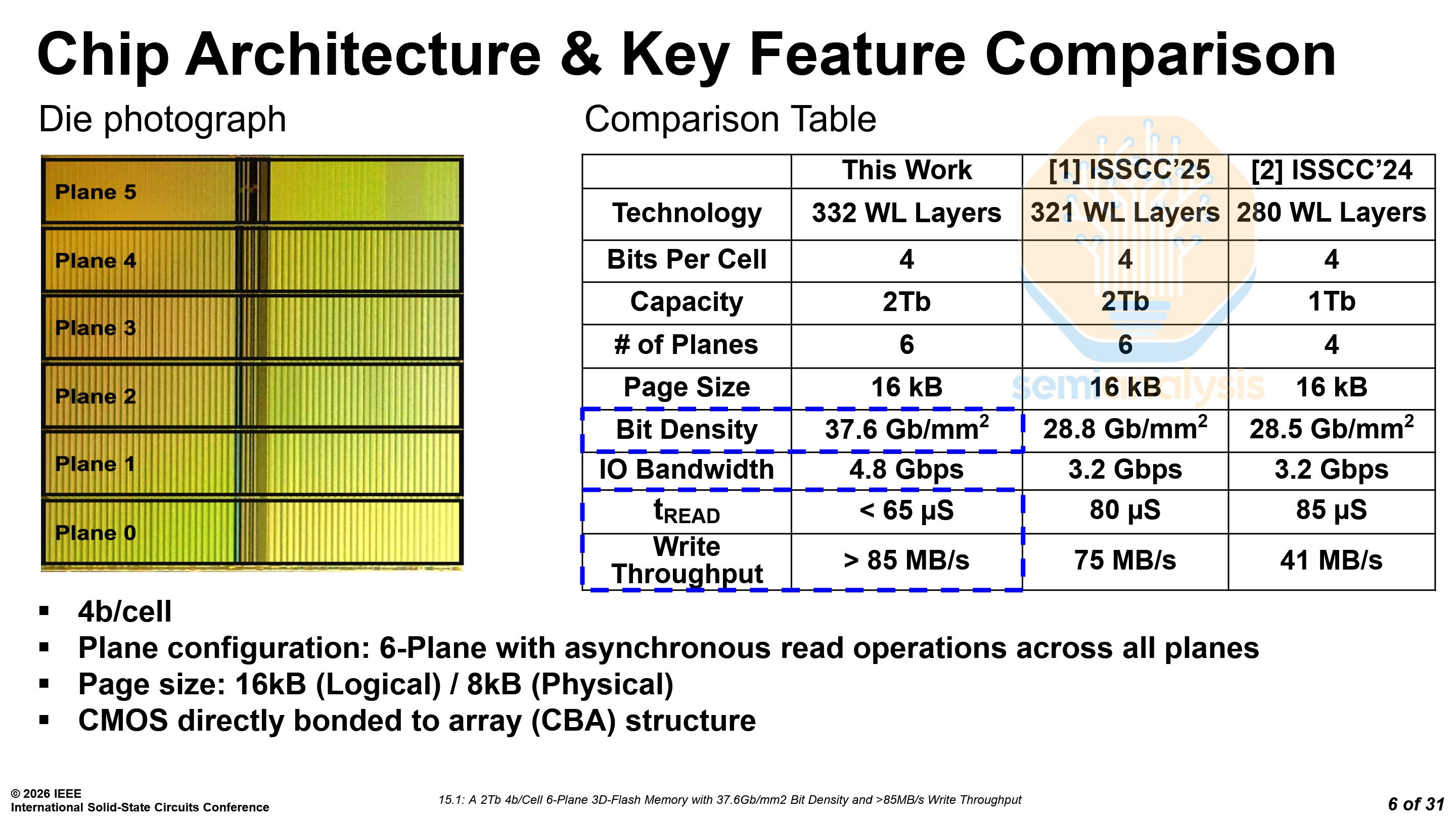
Despite using a similar architecture with 6 planes, 3 decks, and a similar number of layers, SK Hynix falls behind, with 30% lower bit density. In a QLC configuration, BiCS10 has a bit density of 37.6 Gb/mm², while SK Hynix’s V9 has a bit density of only 28.8 Gb/mm². While in a TLC configuration, the densities are 29 and 21 Gb/mm² respectively, another example of SK Hynix’s trailing position.
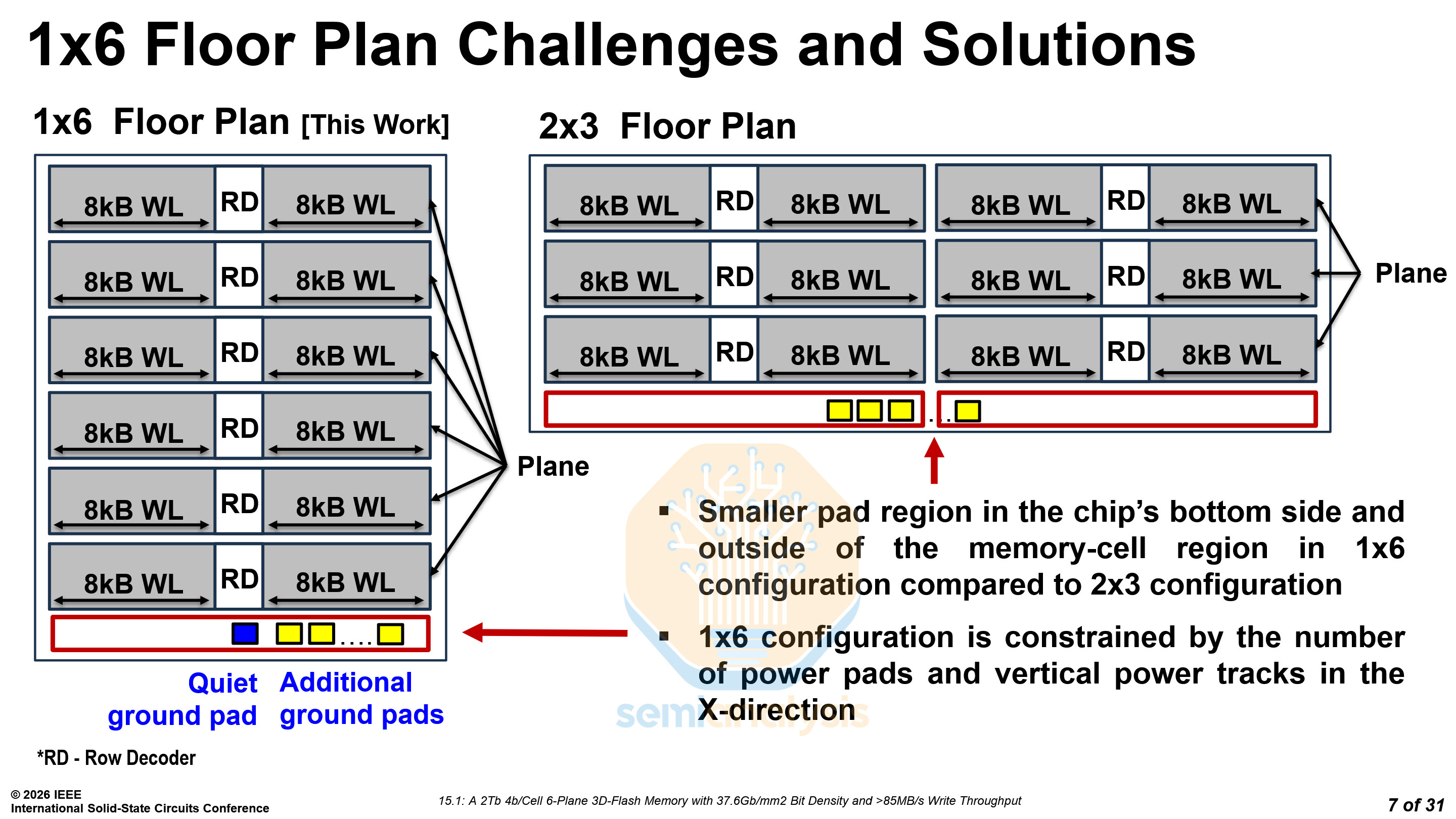
Moreover, BiCS10 features a 6-plane configuration, increasing IO bandwidth by 50%. There are two ways to implement a 6-plane configuration, 1×6 and 2×3. SK Hynix chose to use a 2×3 configuration, while SanDisk and Kioxia have decided to use a 1×6 configuration.
A 1x6 configuration has fewer ground pads and reduces area by 2.1%. However, the lower number of ground pads and vertical power tracks constrains power distribution.
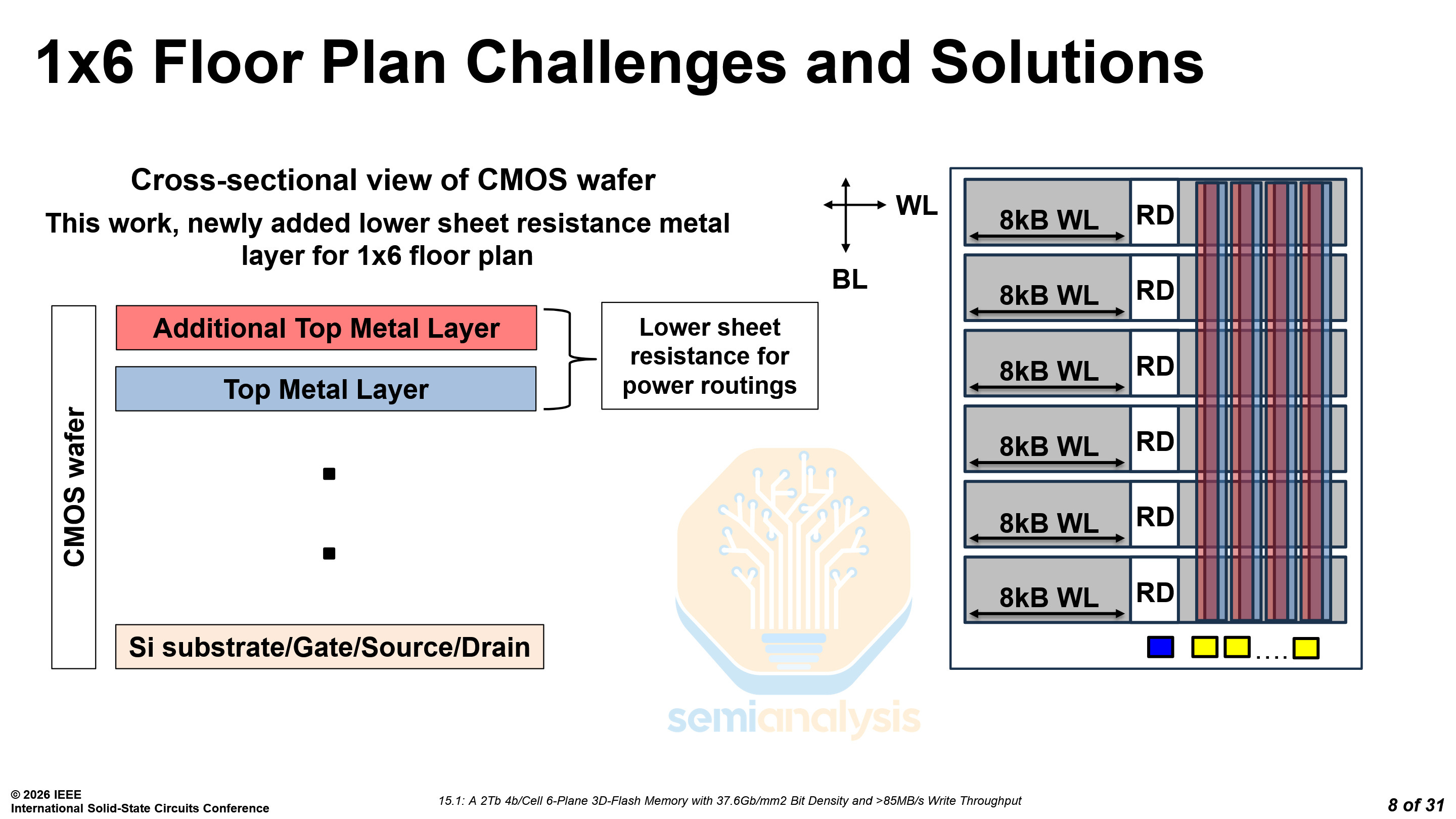
By using the CBA (Cell Bonded Array) architecture, SanDisk and Kioxia are able to customize the CMOS wafer process. By adding another top-metal layer in parallel to the existing one, they created a stronger power grid and overcame their power distribution constraints.
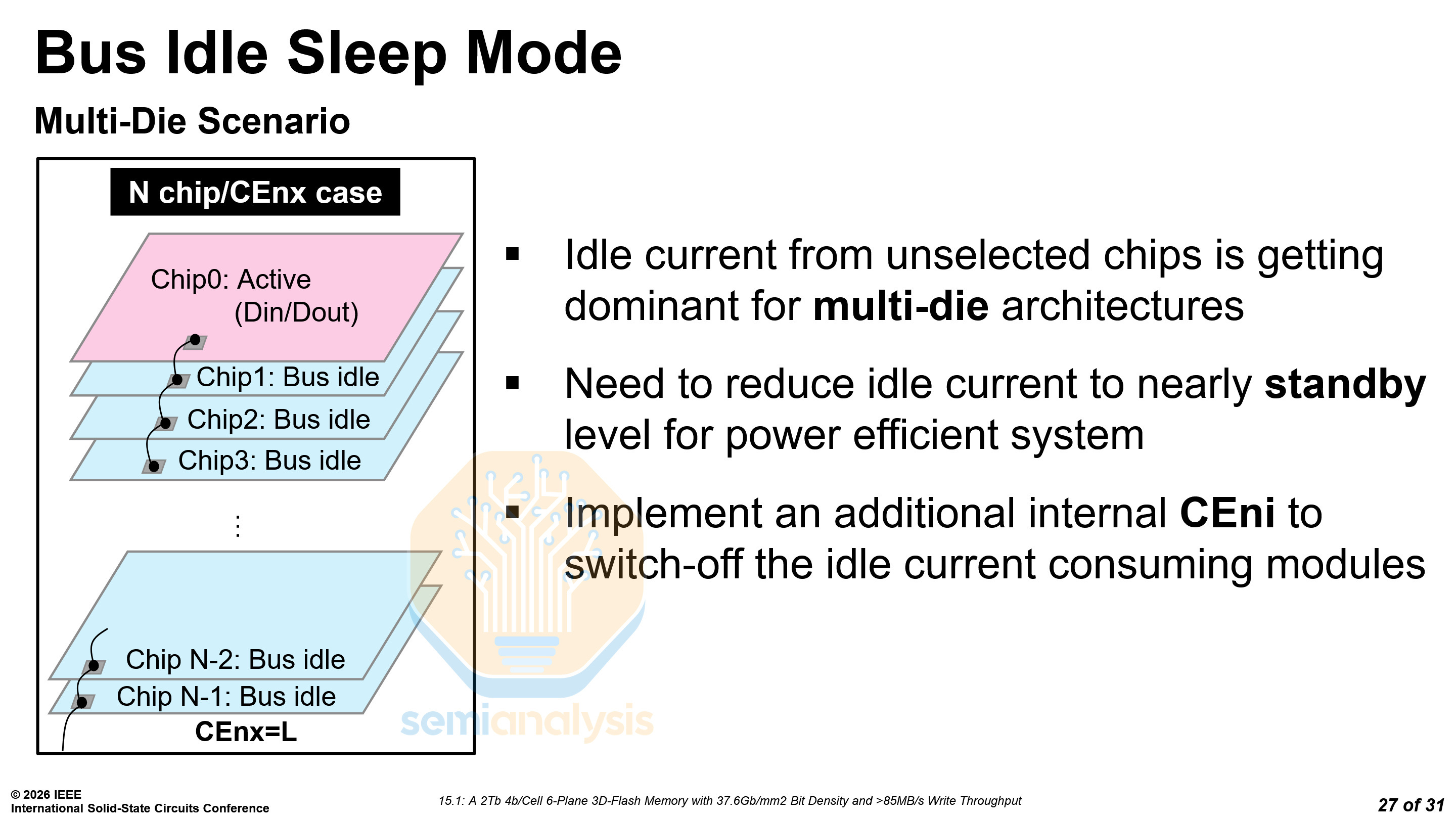
Stacking more dies is essential to increasing storage density. However, in multi-die architectures, the idle current from unselected dies is approaching the active current of the selected die. SanDisk implemented a gating system to fully shut down the data path of the unselected dies, reducing the idle current by two orders of magnitude.
MediaTek xBIT Logic-based Bitcell - Paper 15.2
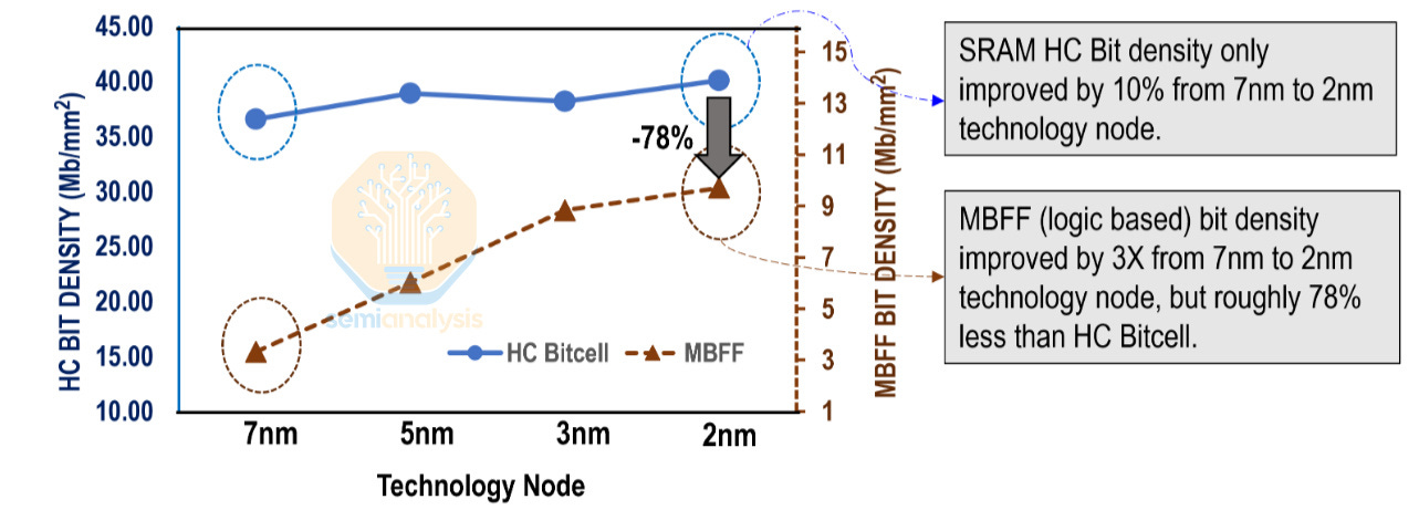
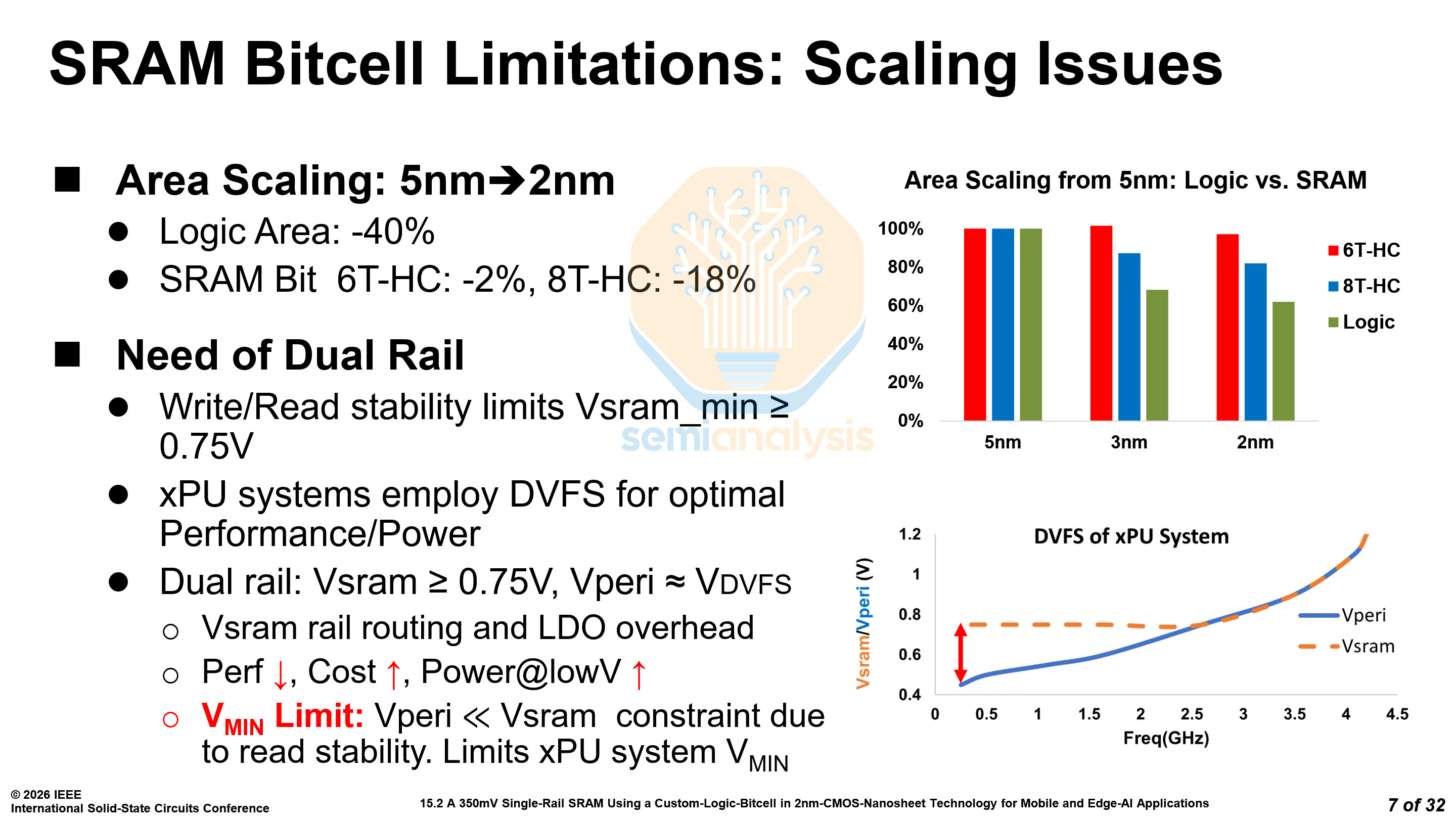
SRAM scaling is dead. Despite logic area decreasing by 40% from N5 to N2, 8-transistor high-current SRAM bitcells have only decreased in area by 18%. 6-transistor high-current (6T-HC) bitcells are even worse, only decreasing by 2%. Assist circuitry has scaled more, but it's not free lunch.
It is well known that N3E’s high-density bitcell is a regression from N3B’s, falling back to N5’s density. In this paper, MediaTek shed some light on the high-current bitcell. N3E’s high-current bitcell increased in area by 1-2% over N5. The density decreased from ~39.0 Mib/mm² to ~38.5 Mib/mm². Do note these figures do not account for assist circuitry overhead.
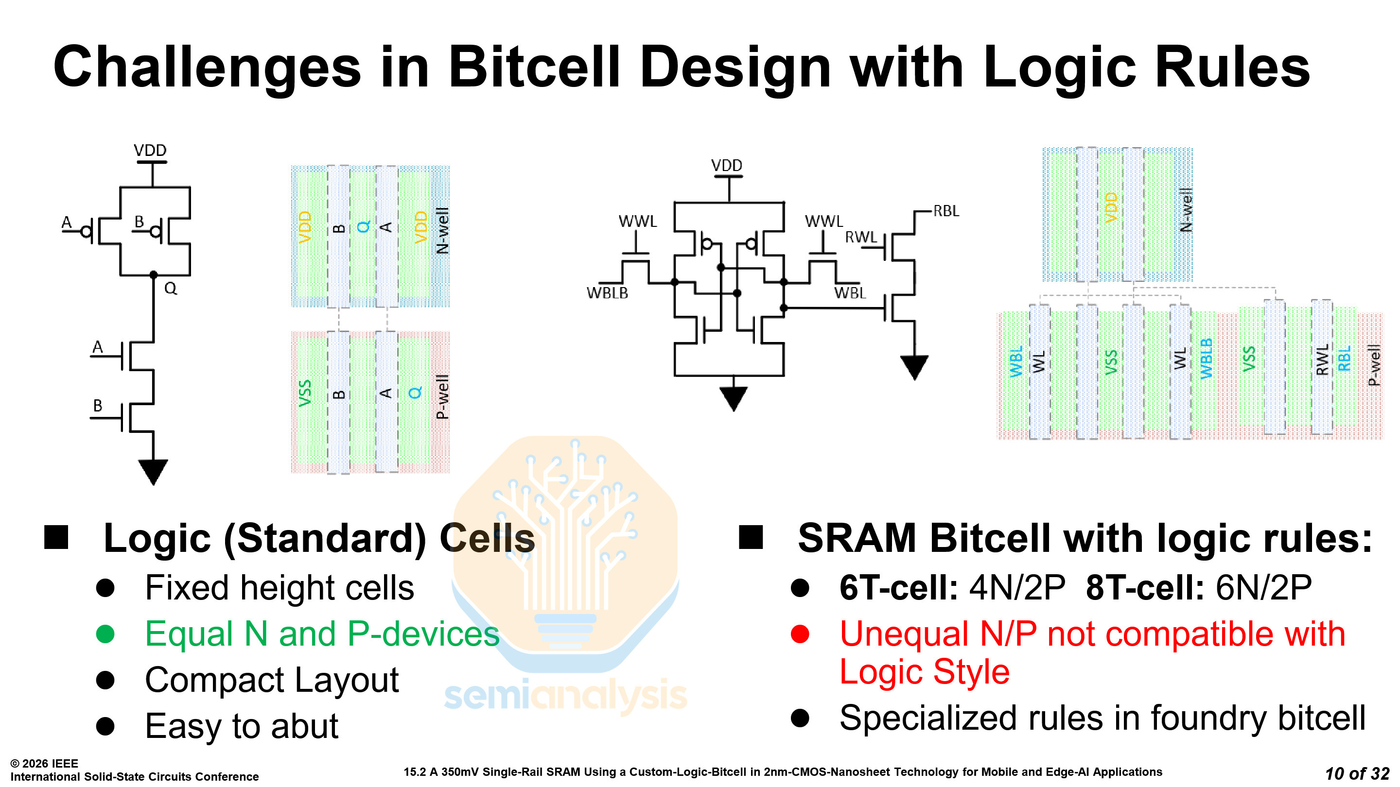
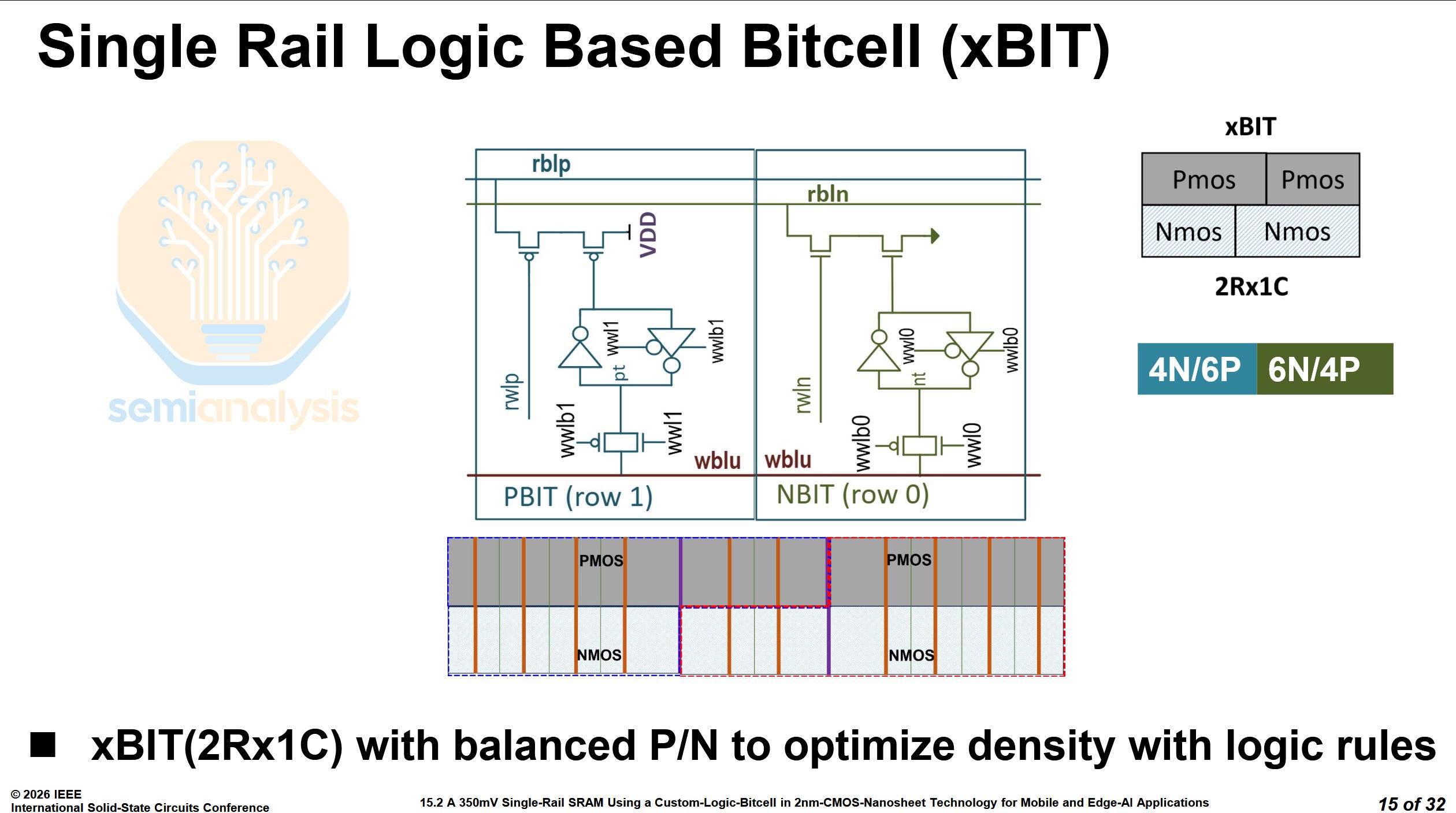
In modern logic nodes, 6T bitcells have 4 NMOS and 2 PMOS transistors, while 8T bitcells have 6 and 2 respectively. The unequal number of NMOS and PMOS transistors requires specialized rules and makes layout more inefficient. MediaTek’s novel bitcell is a 10-transistor cell, named the xBIT, with 4 NMOS and 6 PMOS transistors or vice versa. The two variants of the bitcell can be arranged together into a rectangular block, with 20 transistors, storing 2 bits.
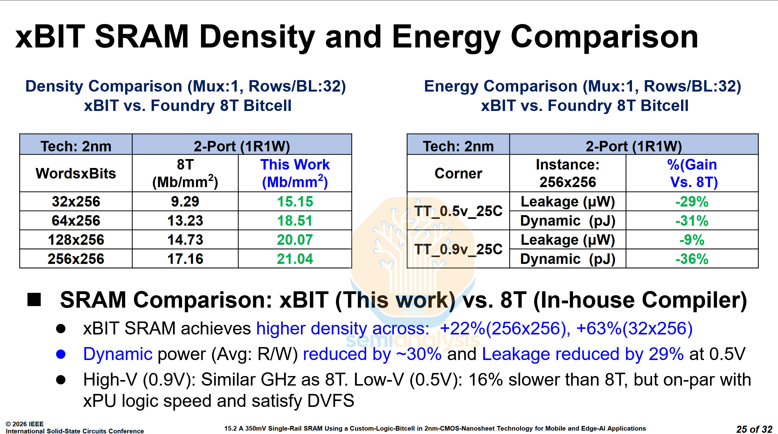
When compared to the PDK’s standard 8T bitcells, the xBIT achieved 22% to 63% higher density, with the largest gains at lower wordline widths. Power has also improved greatly, with the average read/write power reduced by over 30%, and leakage reduced by 29% at 0.5V. At 0.9V, performance was similar to an 8T bitcell and at 0.5V, although it was 16% slower than the 8T bitcell, it was fast enough not to be the bottleneck in a processor, and the voltage range was large enough for voltage-frequency scaling.
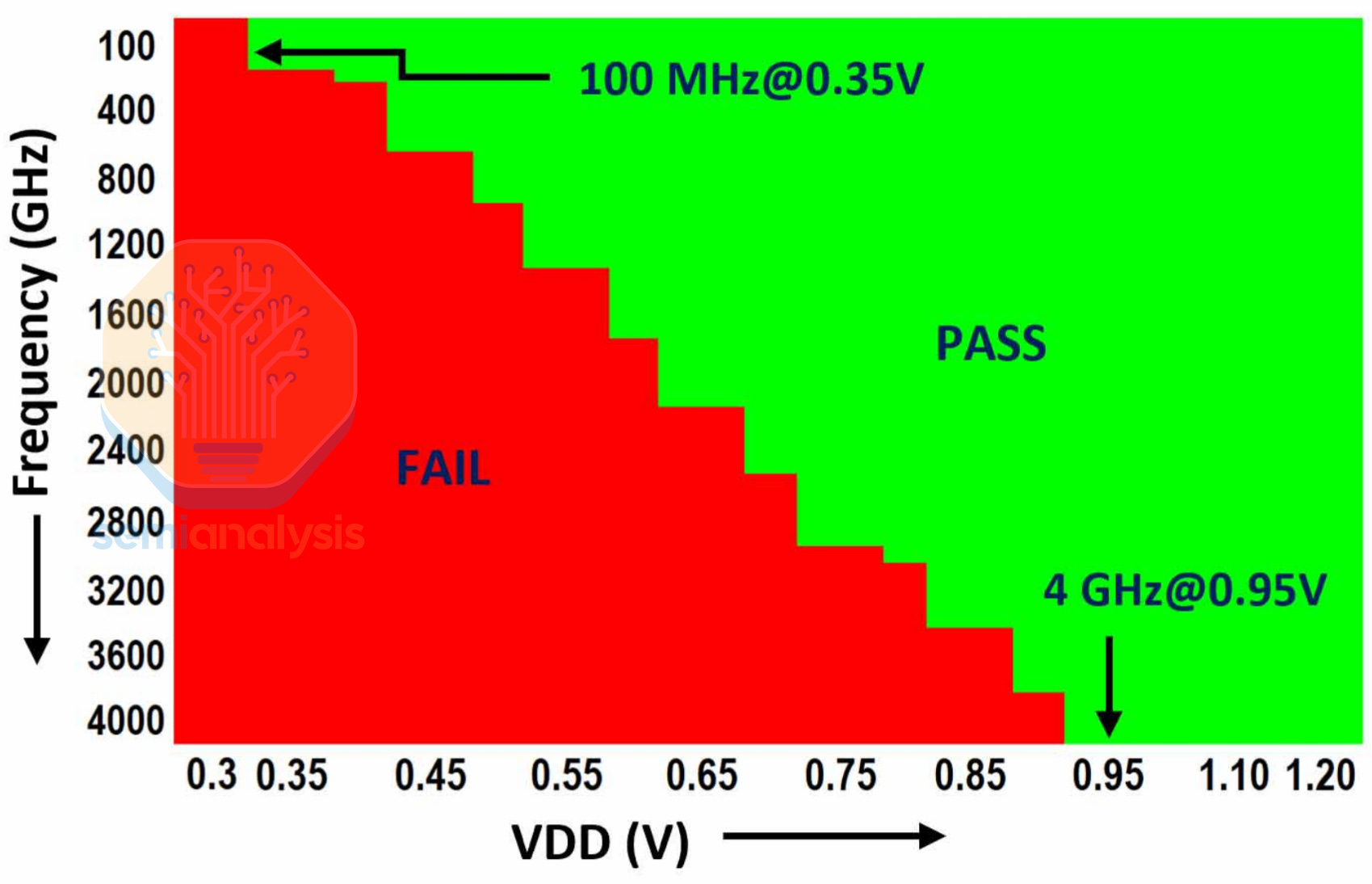
MediaTek also showed a shmoo plot of the xBIT cell, going from 100 MHz at 0.35V, up to 4GHz at 0.95V.
We will be doing a deep dive into SRAM and its scaling factors in an upcoming newsletter article.
TSMC N16 MRAM - Paper 15.4
TSMC presented an updated STT-MRAM on their N16 node, building on their previous work from ISSCC 2023. TSMC is positioning the MRAM as an embedded non-volatile memory (eNVM), for use in automotive, industrial, and edge applications, which do not need the most advanced technology but instead reliability.
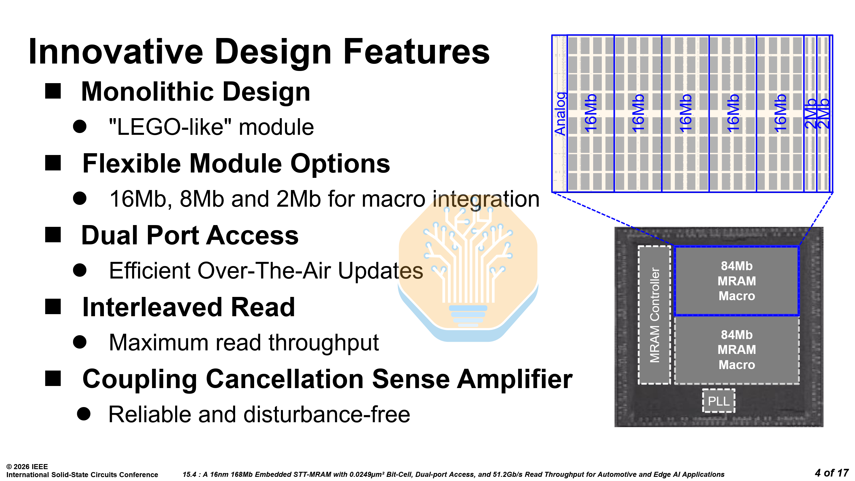
The MRAM features dual-port access so reads and writes can occur simultaneously — critical for over-the-air (OTA) updates in automotive, where the system cannot halt reads while firmware is being written.
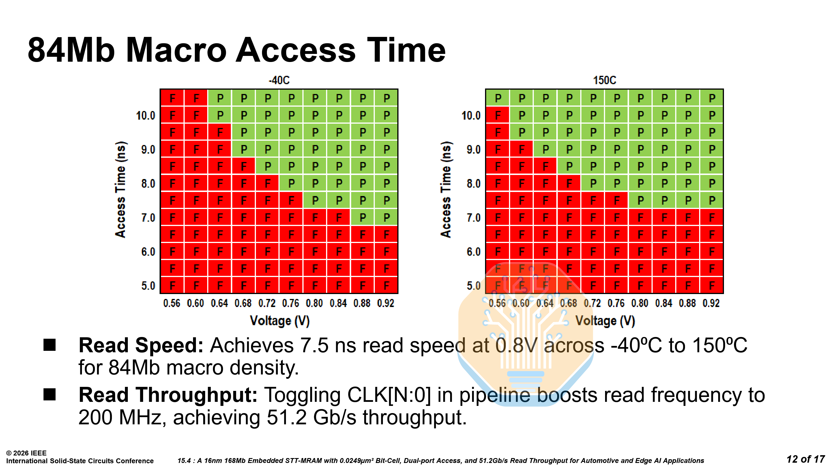
It features interleaved reads across modules with independent clocks, raising throughput to 51.2 Gb/s at 200 MHz. On silicon, the 84 Mb macro achieves 7.5ns read access time at 0.8V across -40 °C to 150 °C.
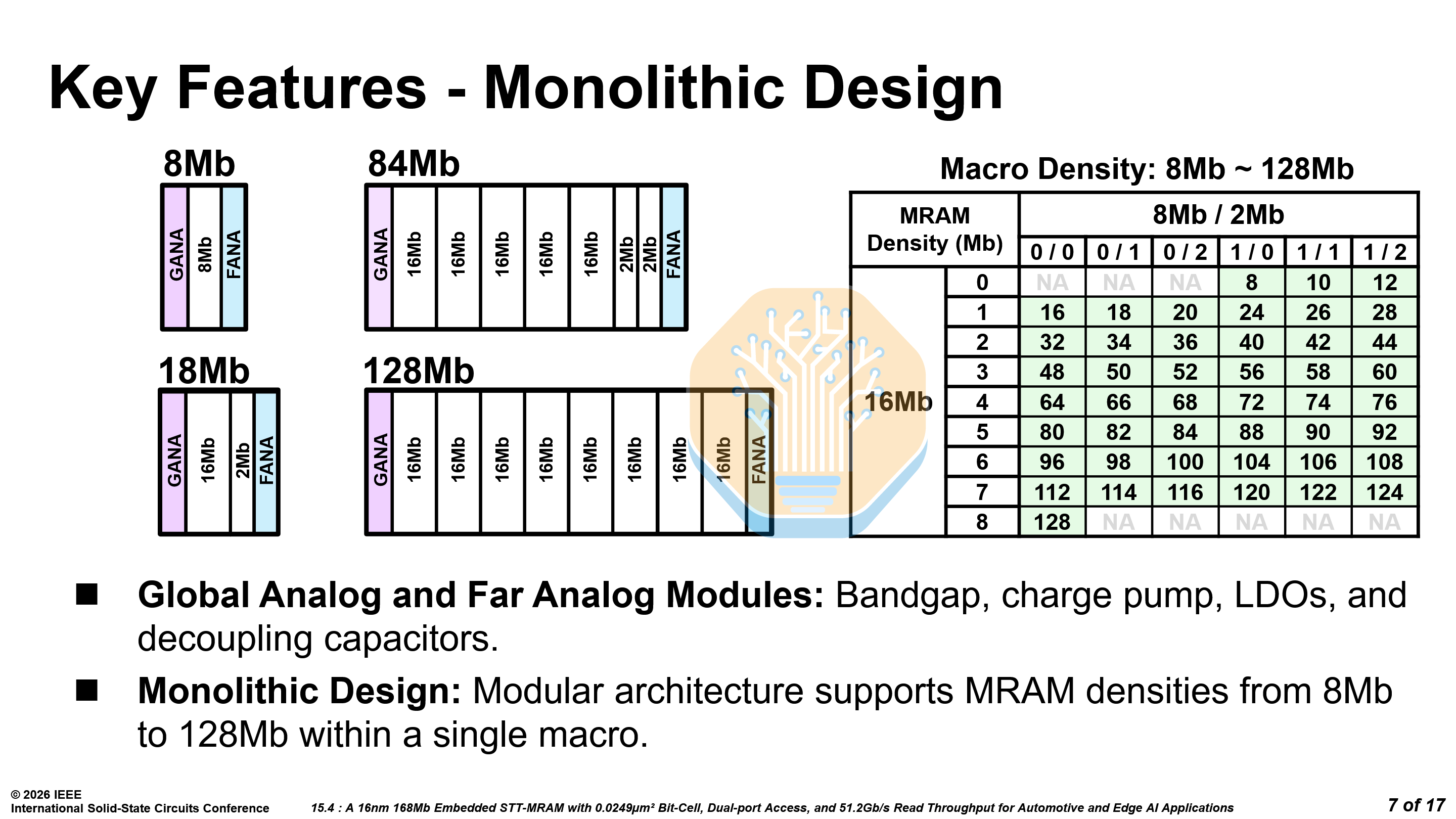
The architecture is modular — configurable in 16 Mb, 8 Mb and 2 Mb modules that compose into macros from 8 Mb to 128 Mb. By combining large 16 Mb modules with a few smaller 2 Mb and 8 Mb modules, the capacity can be fine tuned to the needs of any design. For example, 5× 16 Mb modules and 2× 2 Mb modules form an 84 Mb macro.
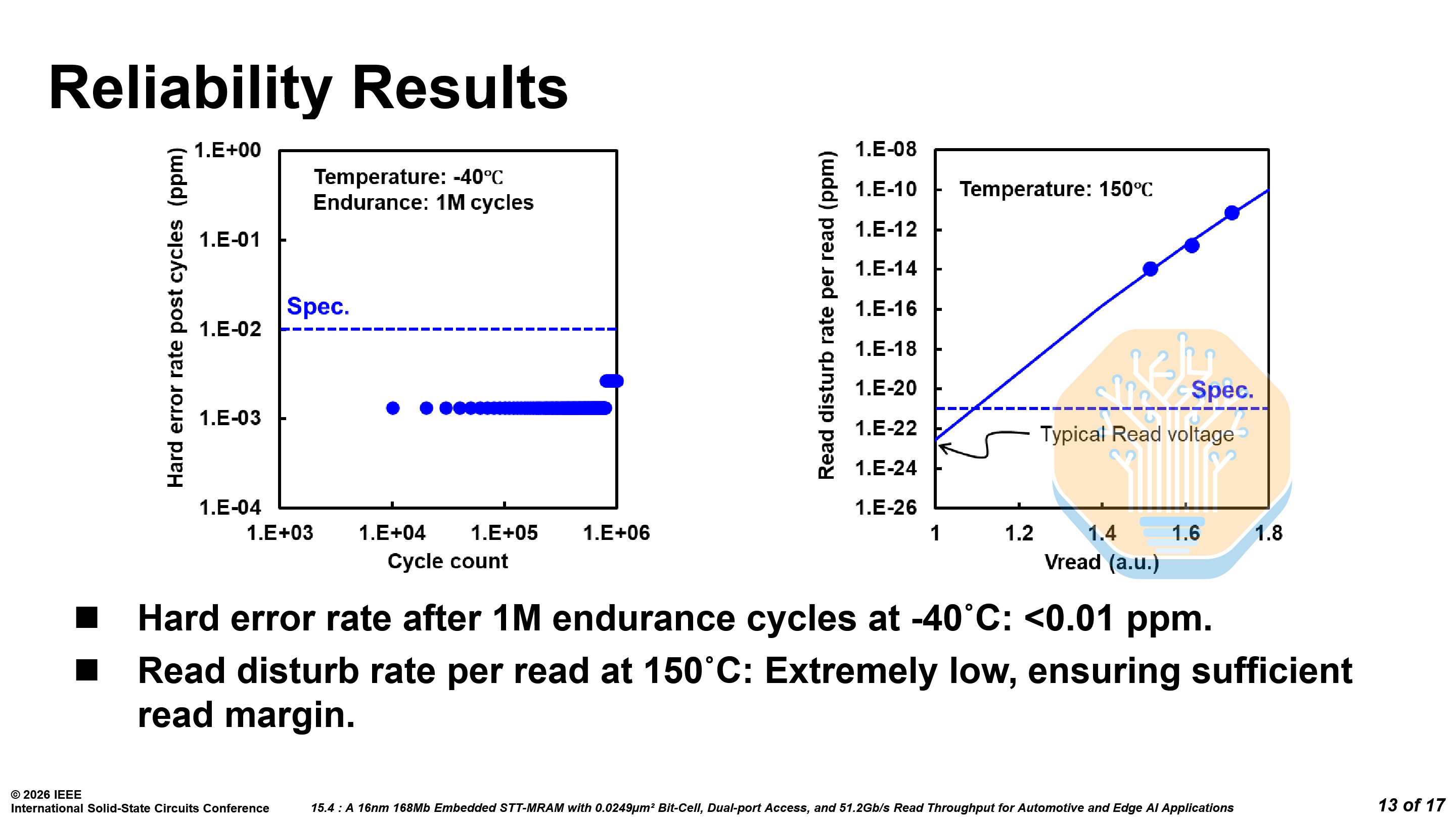
As stated earlier, reliability is where embedded MRAM lives or dies. After 1 million endurance cycles at -40 °C, the hard error rate stays well below 0.01 ppm — well within ECC correction range. Read disturb at 150 °C is below 10⁻²² ppm at typical read voltages, effectively negligible. The 168 Mb test chip passes reflow and supports 20-year retention at 150 °C, meeting stringent automotive requirements.
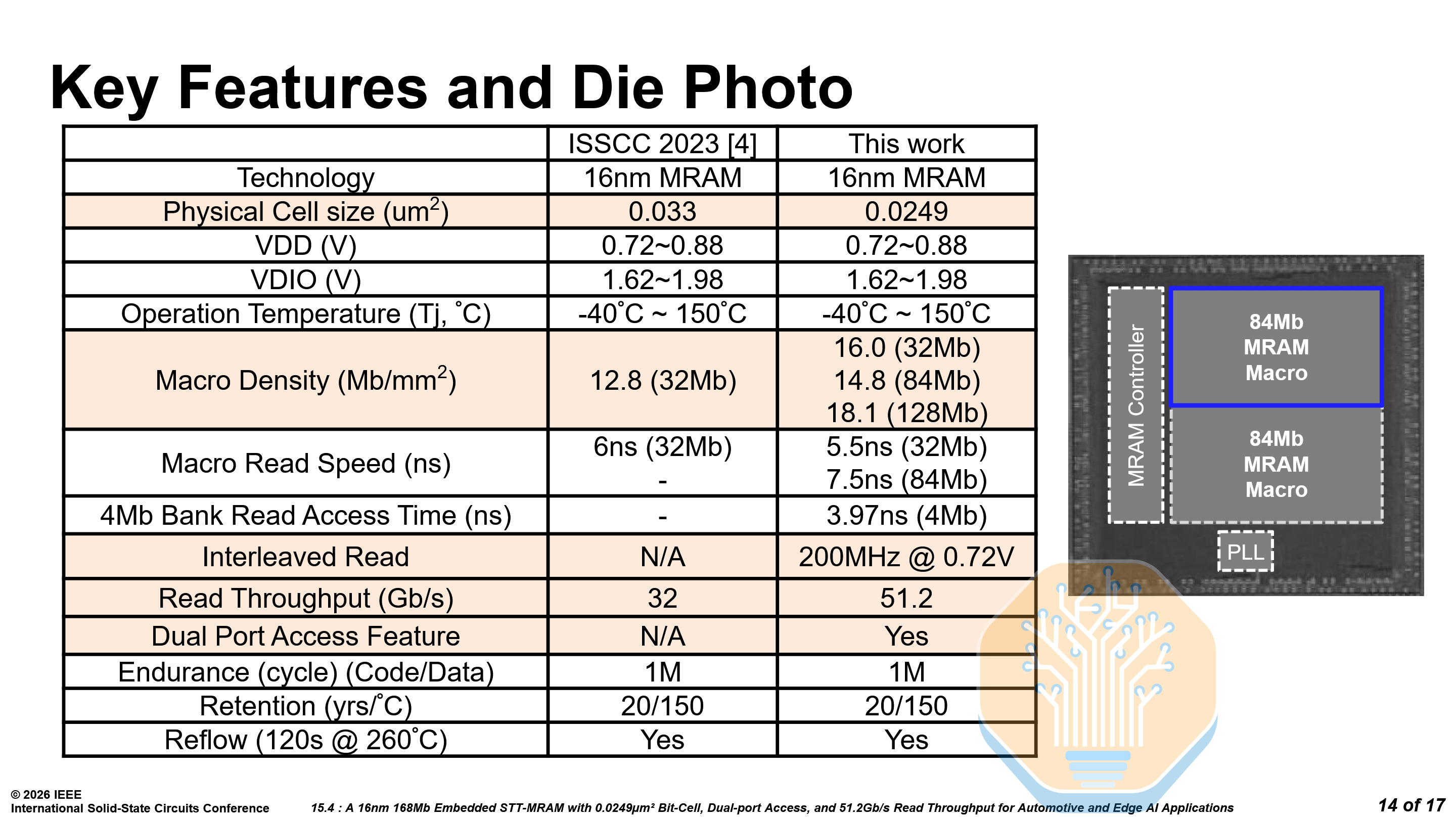
Compared to the old MRAM on the same N16 node, the bitcell has shrunk 25% from 0.033 µm² to 0.0249 µm², and macro density increases to 16.0 Mb/mm² iso-capacity. The read speed drops from 6 ns to 5.5 ns iso-capacity, and the dual-port access and interleaved reads are entirely new.
While Samsung Foundry also published work on 8LPP eMRAM this year, TSMC’s is far more promising. It targets the needed features, has great performance, and is on a cheaper N16 node.
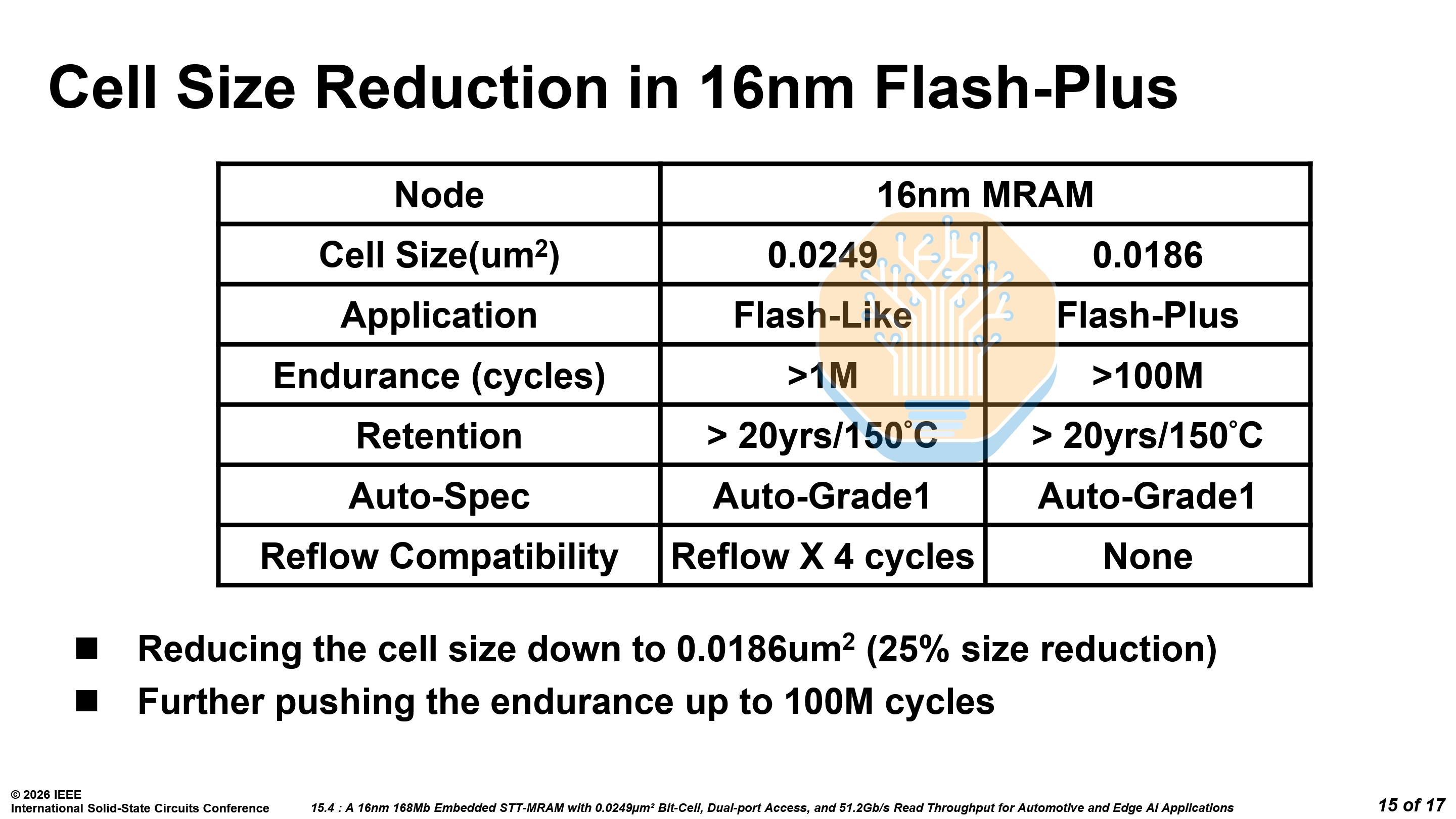
TSMC is already planning the next-generation “Flash-Plus” variant with a 25% smaller bitcell and 100× higher endurance.
Optical Networking
Several papers from major optics vendors tackled optical interconnects that will carry data between next-generation AI accelerators both within and between datacenters.
Nvidia DWDM - Paper 23.1
The choice of optical signaling format will affect the go-to-market timeline for scale-up co-packaged optics (CPO). Nvidia is ramping up production of COUPE optical engines that support 200G per lane PAM4 for scale-out switching in the near-term.
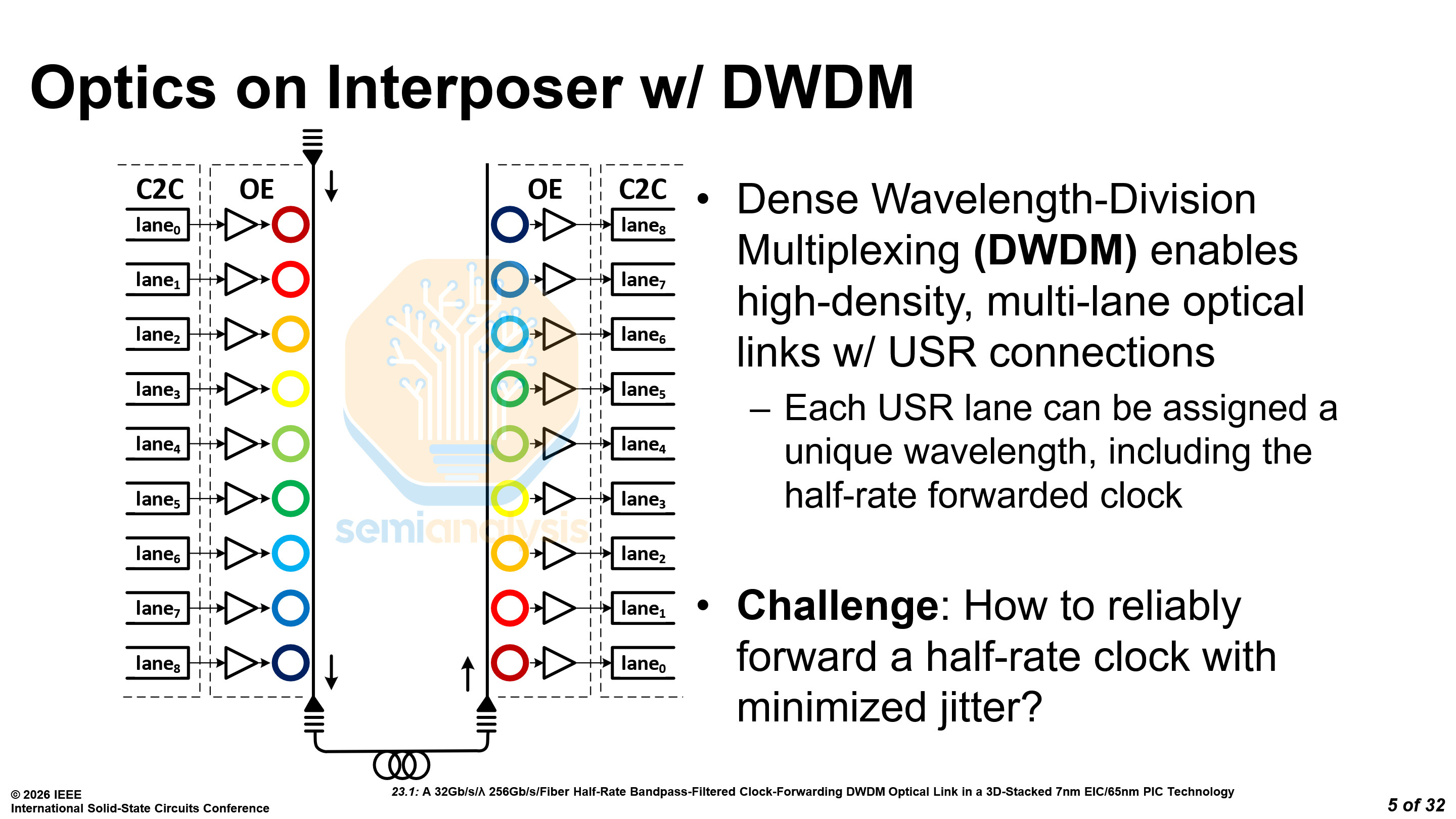
However, at ISSCC, Nvidia proposed using 32 Gb/s per lambda, with 8 wavelengths multiplexed using DWDM. A 9th wavelength is used for clock forwarding at half rate — that is 16 Gb/s.
Clock forwarding means that SerDes can be made somewhat simpler by removing the Clock and Data Recovery (CDR) circuit as well as other circuitry, improving energy and chip shoreline efficiency.
Earlier in March, just before OFC 2026, the formation of the Optical Compute Interconnect MSA (OCI MSA) was announced, and it will focus on a 200 Gb/s Bi-directional link, with each of transmit and receive formed using 4 lambdas of 50G NRZ, which will be sent bi-directionally across the same fiber. Did I hear anyone mention OCS?
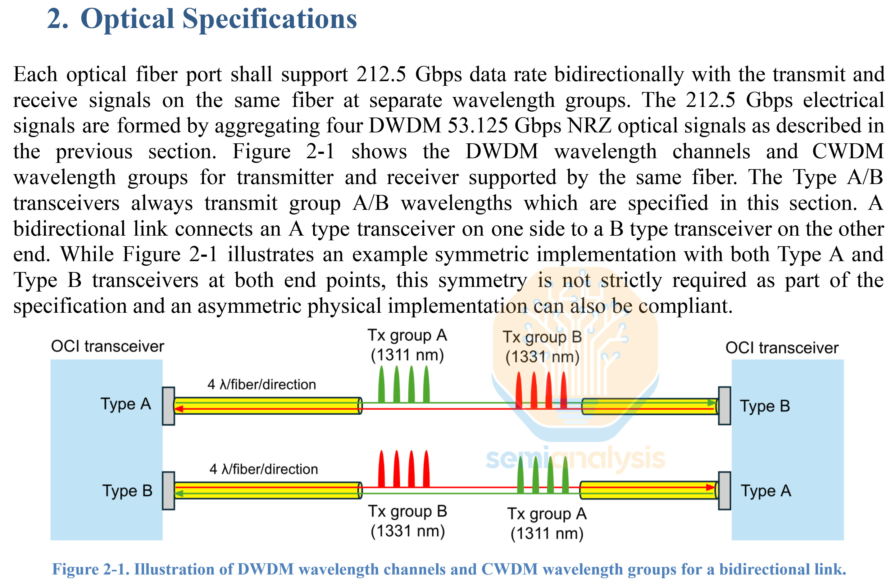
Interestingly, the OCI MSA did not make use of an additional wavelength for clock forwarding, and it appears that reserving all wavelengths for actual data transmission is the priority.
Much of Nvidia’s published research on scale-up CPO has centered on DWDM, though today’s CPO optical engines are oriented around 200G PAM4 DR Optics, which makes more sense for scale-out networking. The OCI MSA centering around DWDM for scale-up optics resolves this apparent contradiction, as it is now clear that Nvidia and others will center around the use of DWDM for scale-up and DR Optics for scale-out.
The OCI MSA also illustrates different implementations, an On-Board Optics (OBO), a version of CPO that is integrated via the substrate on the ASIC package, and a version where the optical engine is integrated directly on the interposer. The implementation illustrated in the middle figure (b) will be the most common one used for scale-up and scale-out CPO for the next few years, but it still requires some form of serialized links that can pass through the ASIC substrate and will still require some form of SerDes on both sides. For example, UCIe-S could be used as a protocol for such transmission.
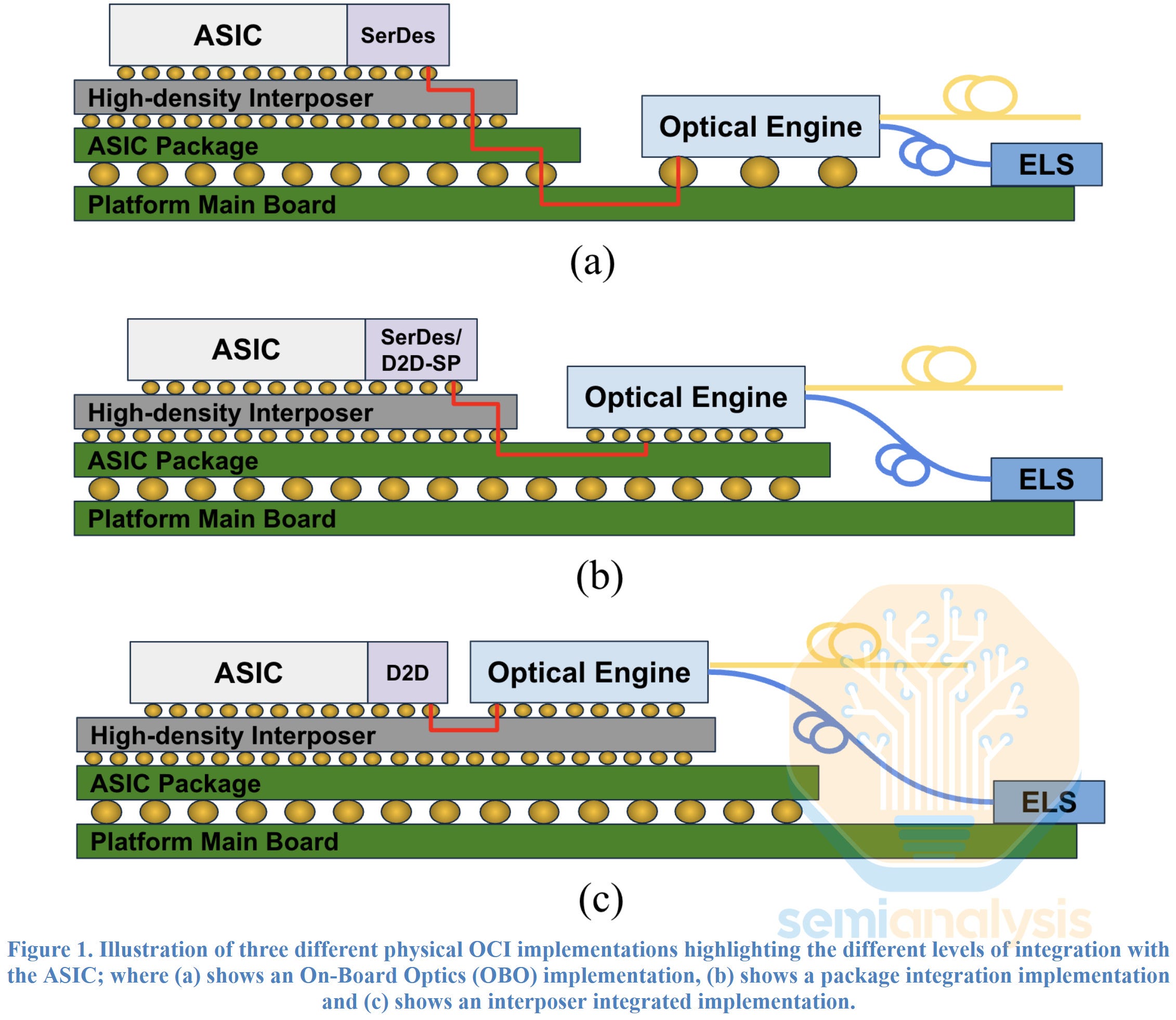
The “Final Boss” when it comes to implementing CPO will be when the optical engine can be integrated onto the interposer itself, connecting to the ASIC using a parallelized die to die (D2D) connection as depicted in (c) above. This could considerably improve shoreline bandwidth density, enable much higher radix and improve energy efficiency. This implementation thus unlocks benefits of CPO in ways that the other implementations cannot, but achieving it is still a few years away and requires further improvements in advanced packaging technology.
Marvell Coherent-Lite Transceiver - Paper 23.2
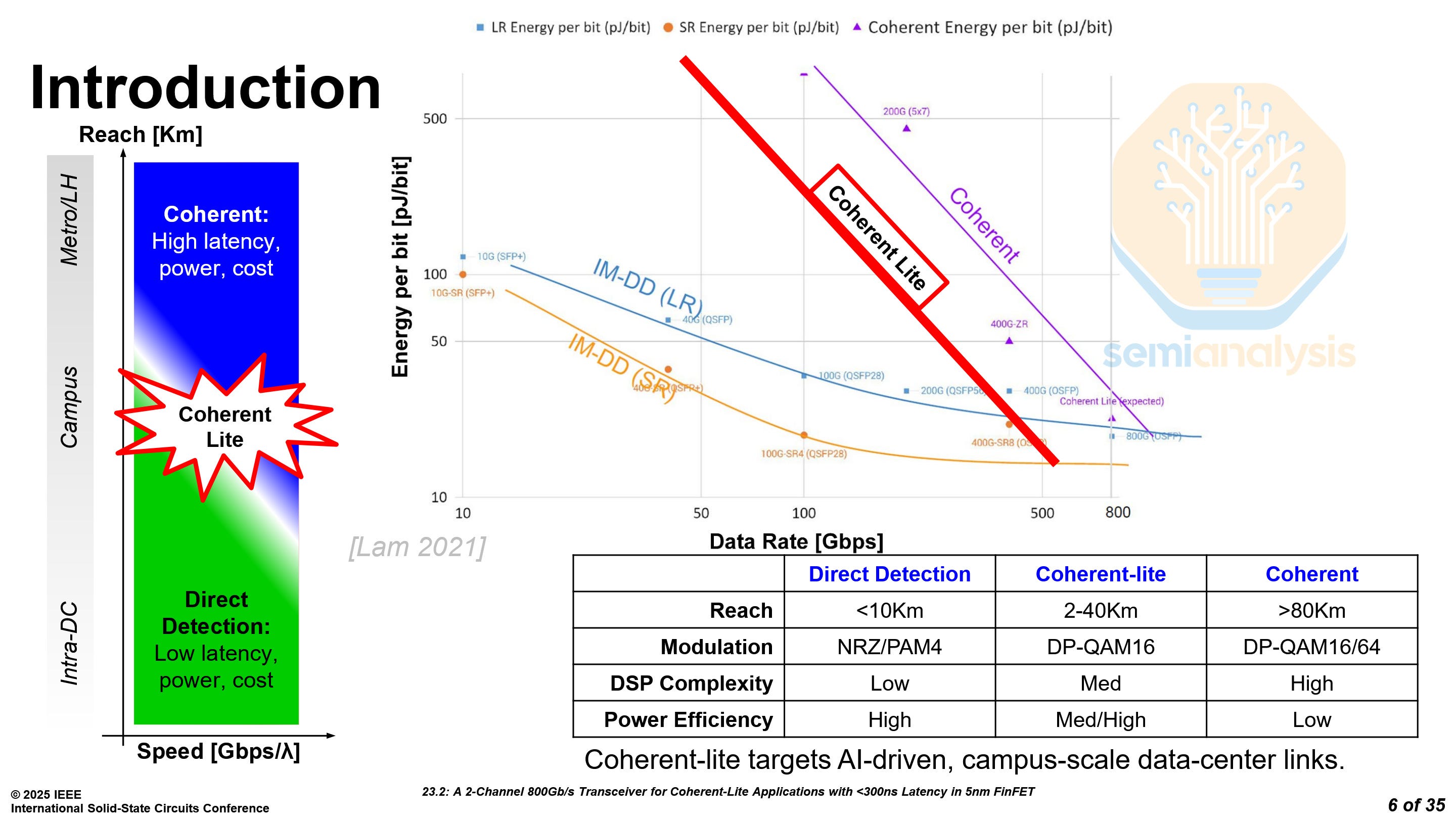
Marvell presented an 800G transceiver for coherent-lite applications. Traditional transceivers have a limit on how far they can reach, less than 10 kilometers. Coherent transceivers support much further reach, but they are complex, consume more power, and are more expensive. Marvell’s Coherent-lite transceiver targets a middle ground with respect to power consumption, cost and range, which is perfect for large datacenter campuses with links spanning at most tens of kilometers.
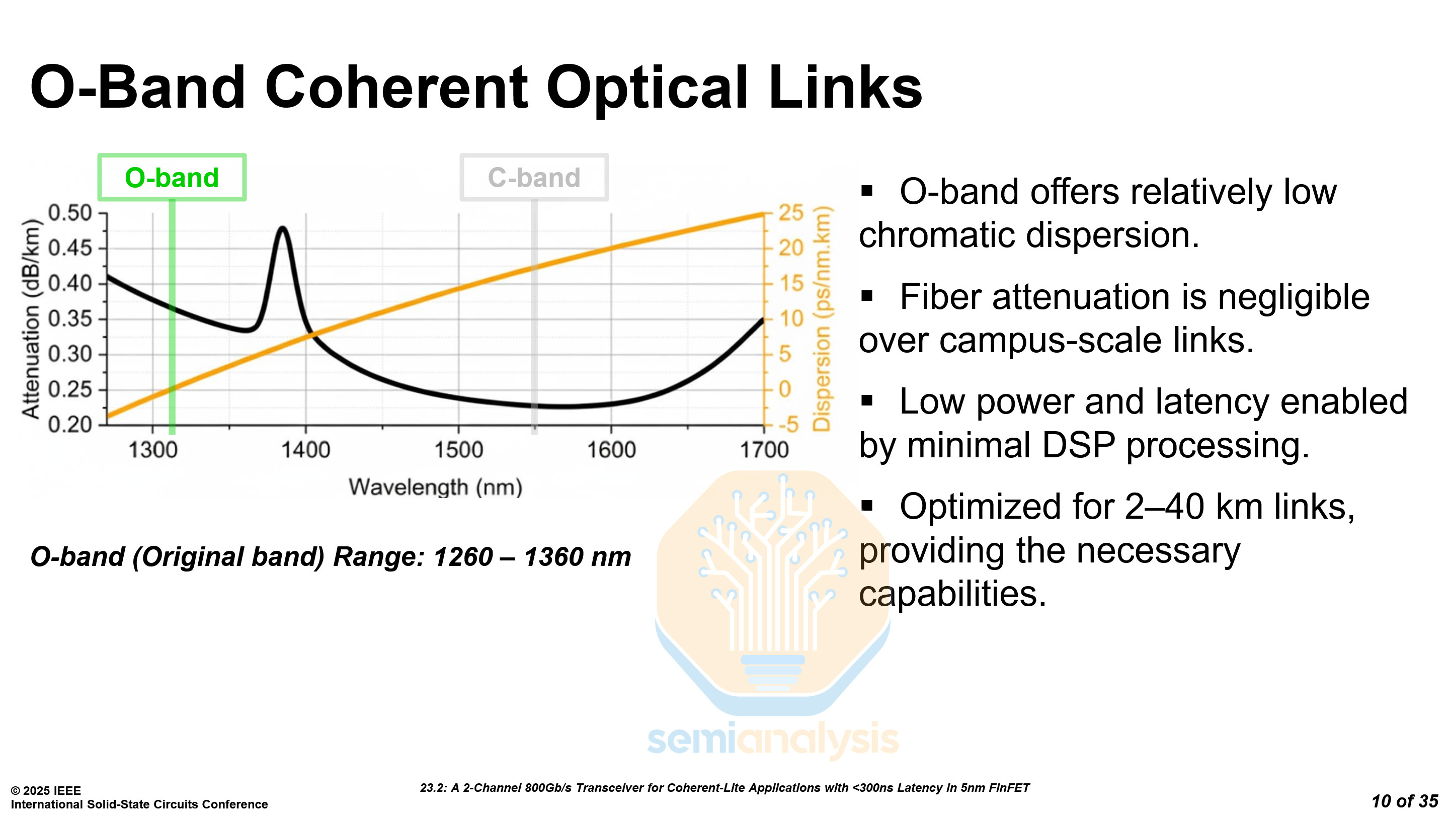
Coherent transceivers primarily use C-band wavelengths for their low attenuation. However, the long-haul links in which coherent transmission is used typically have a very high dispersion, needing heavy DSP processing. The long range of traditional Coherent optics can often be overkill for datacenter campuses with buildings that are only tens of kilometers apart.
Coherent-Lite transceivers instead use O-band wavelengths, which have near-zero dispersion over the relatively short distances on a datacenter campus. This enables minimal DSP processing, saving power and reducing latency.
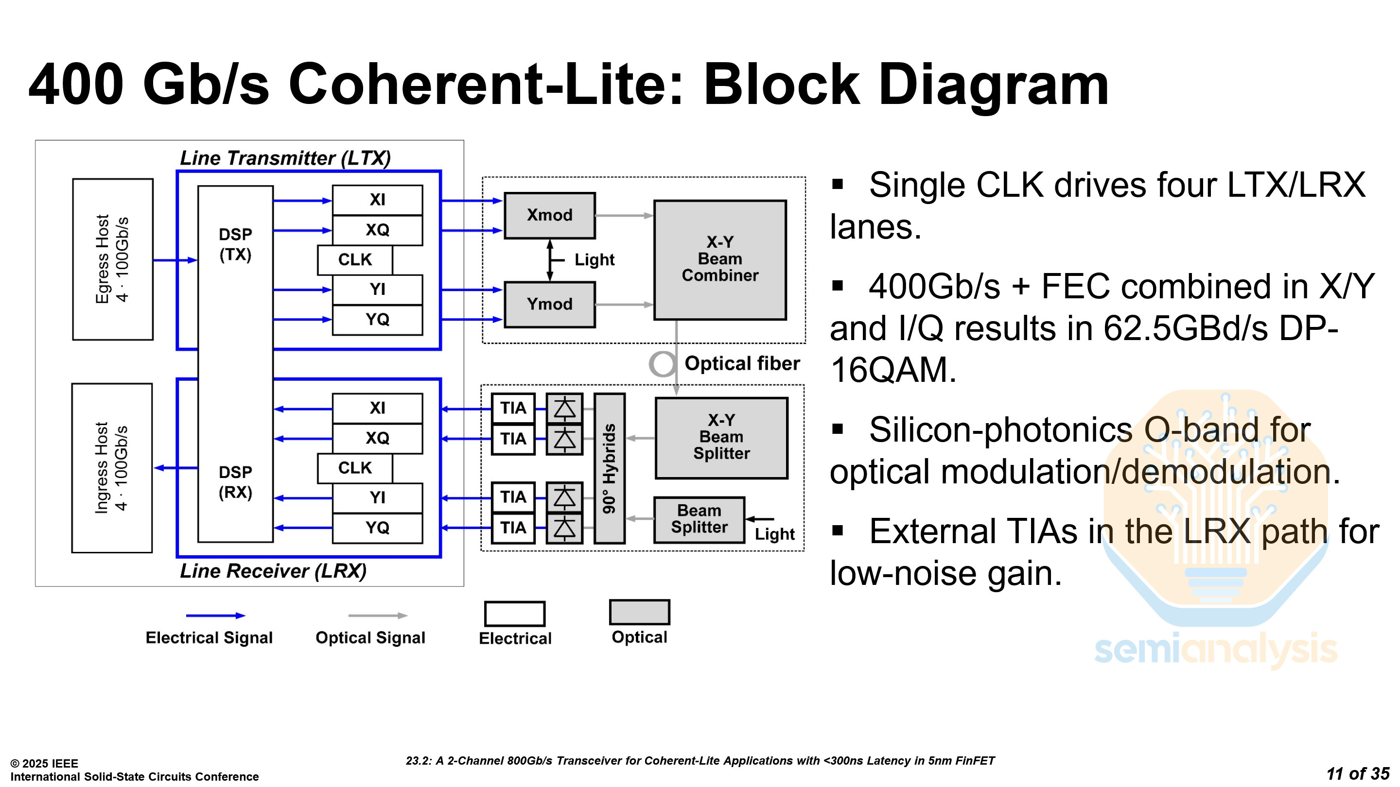
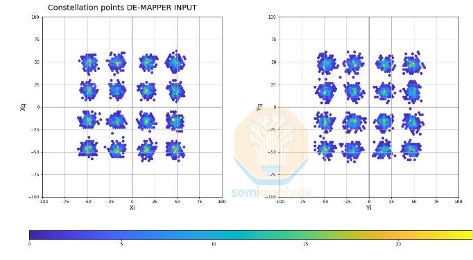
The Coherent-lite transceiver is a DSP-based pluggable module consisting of two 400G channels. Each 400G channel runs a dual polarization QAM and consists of two parallel modulation streams, X and Y.
The key to this demonstration is highlighting other methods of scaling channel bandwidth that are optimized for the campus application.
Higher-order modulation coupled with the dual polarization using X and Y axes delivers 400G channel bandwidth. There are 8 bits per channel for a total of 32 constellation points as demonstrated above. These 8 bits times the 62.5 GBd signal rate equals ~400G of total bandwidth.
This modulation scheme is not entirely new to the industry, but it is now being brought into the datacenter campus setting for use in those shorter links.
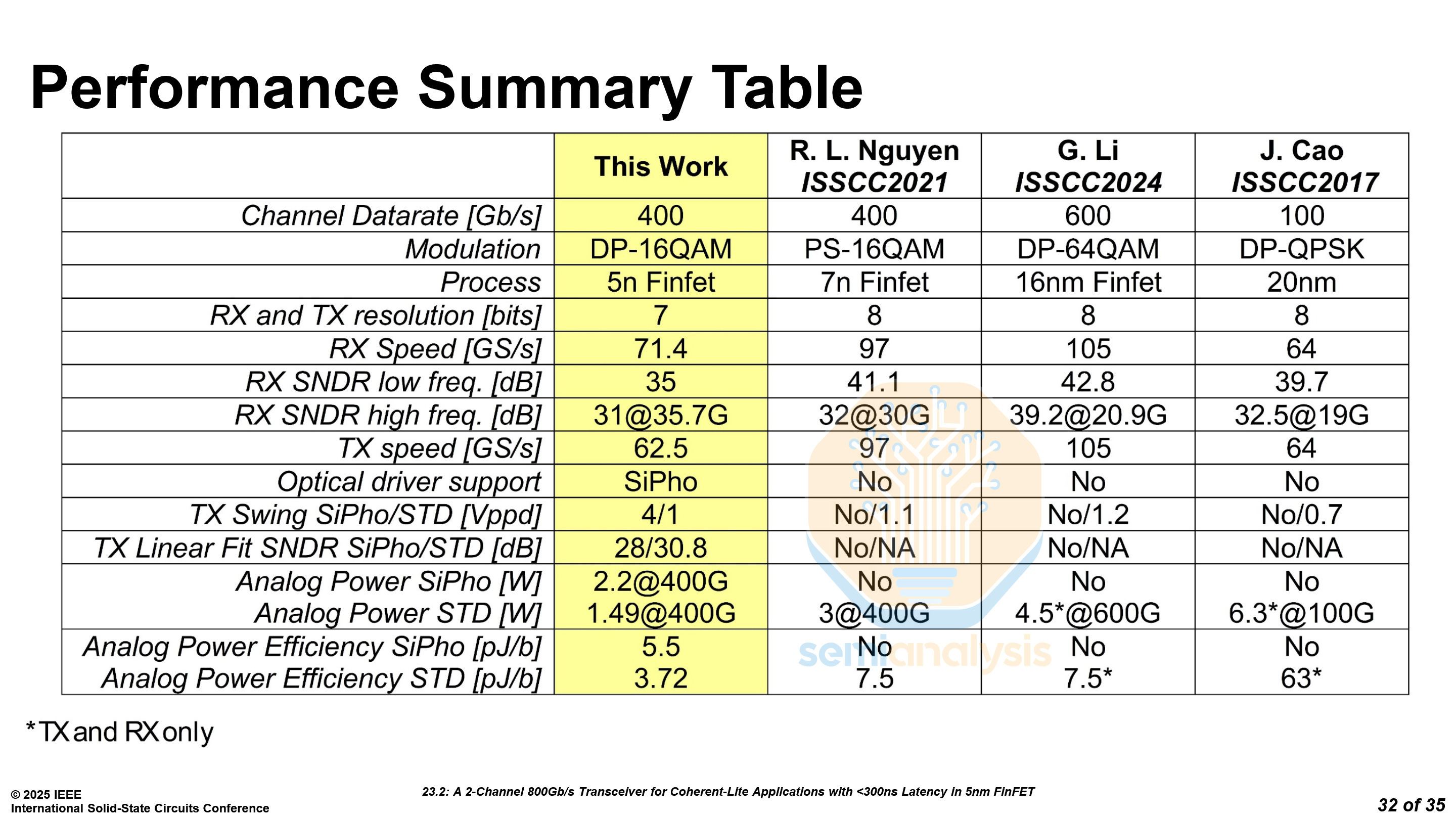
Marvell’s approach significantly reduces power to only 3.72 pJ/b excluding silicon photonics, half of other full-fledged coherent transceivers. Their measurements were taken over a fiber length of 40km, with a latency of less than 300 ns.
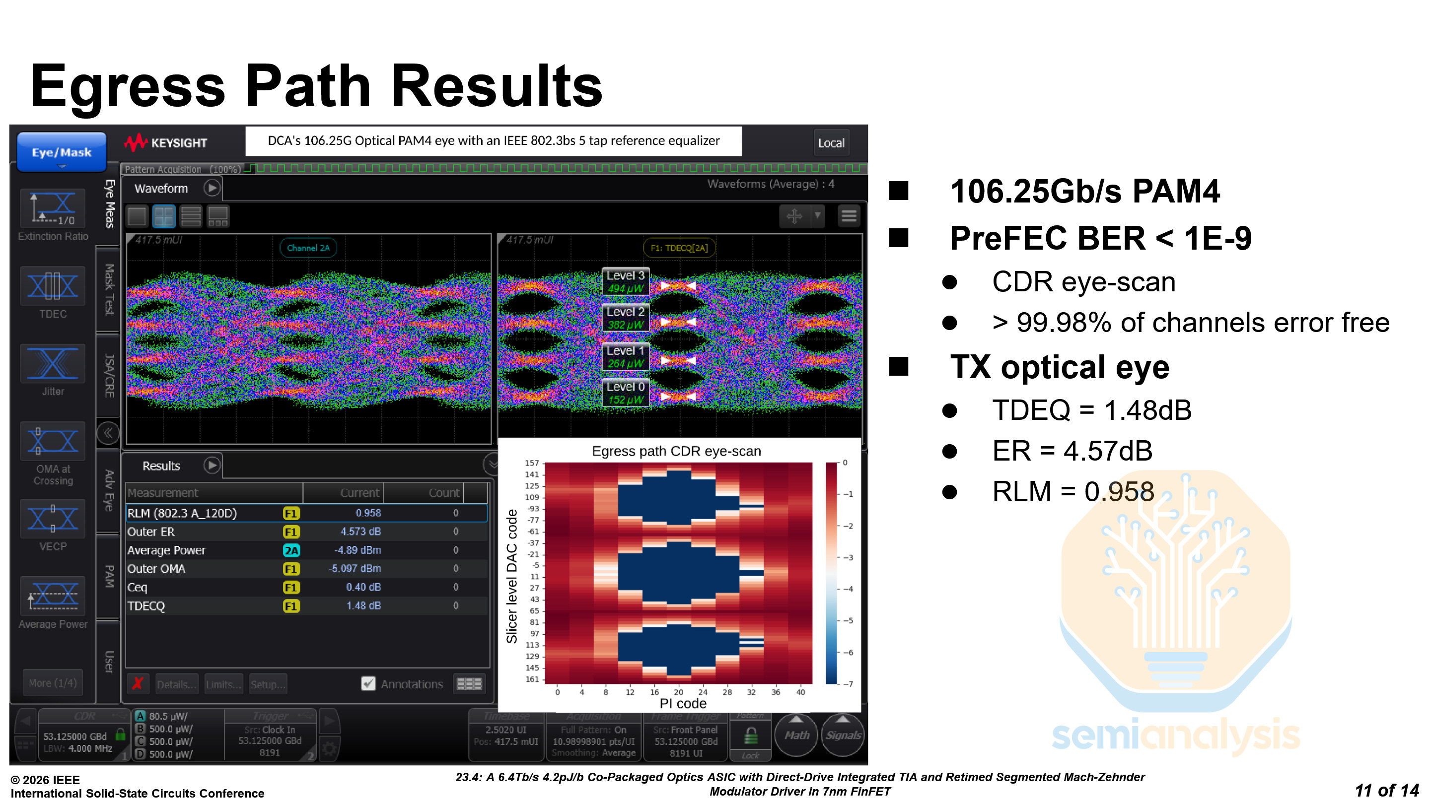
Broadcom 6.4T Optical Engine - Paper 23.4
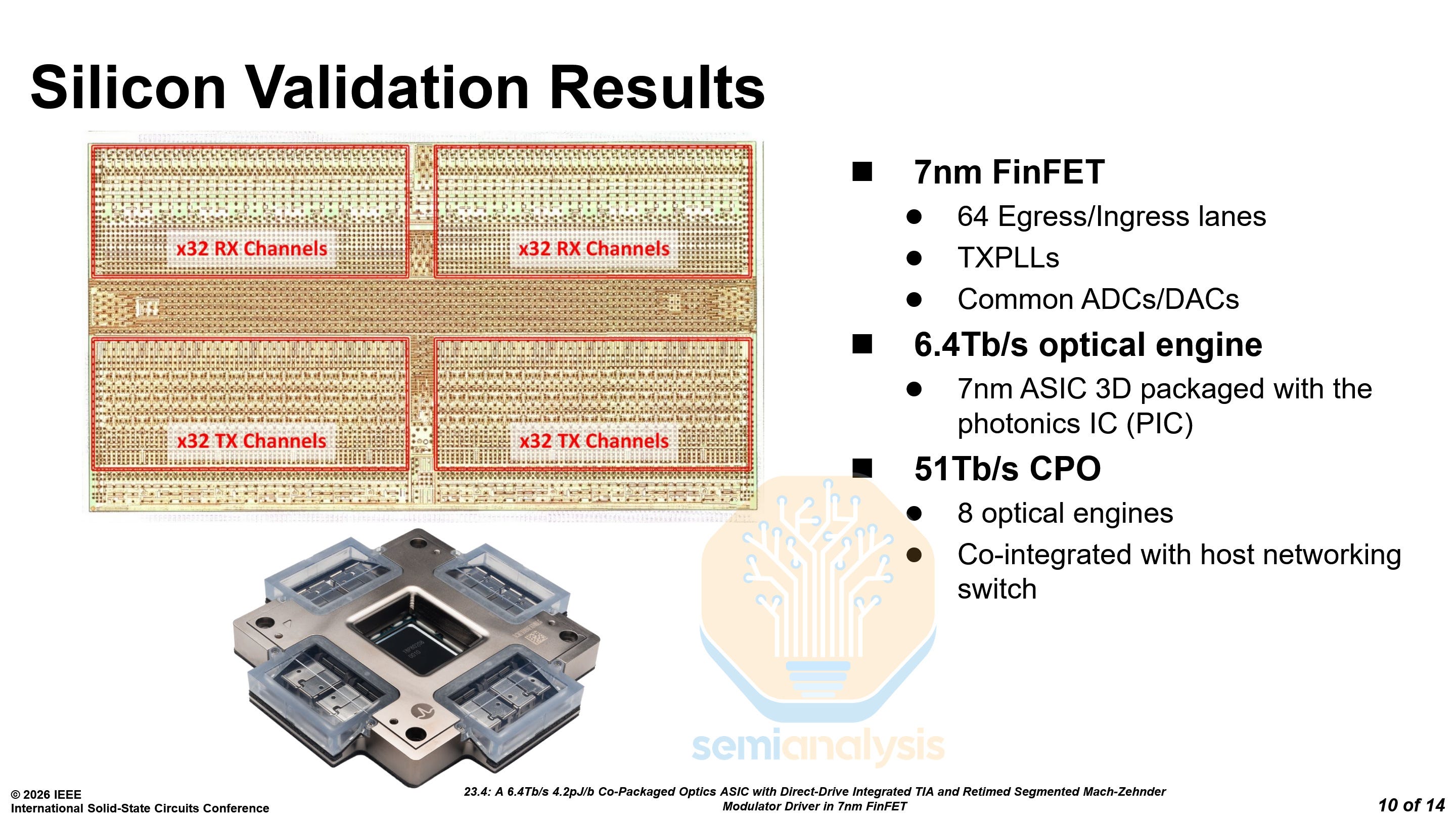
Broadcom showcased progress on their 6.4T MZM optical engine (OE) consisting of 64 lanes of ~100G using PAM4 modulation. The optical engines were tested in a Tomahawk 5 51.2T CPO system. One CPO package consists of eight 6.4T OEs, each with a PIC and an EIC, on TSMC’s N7 process.
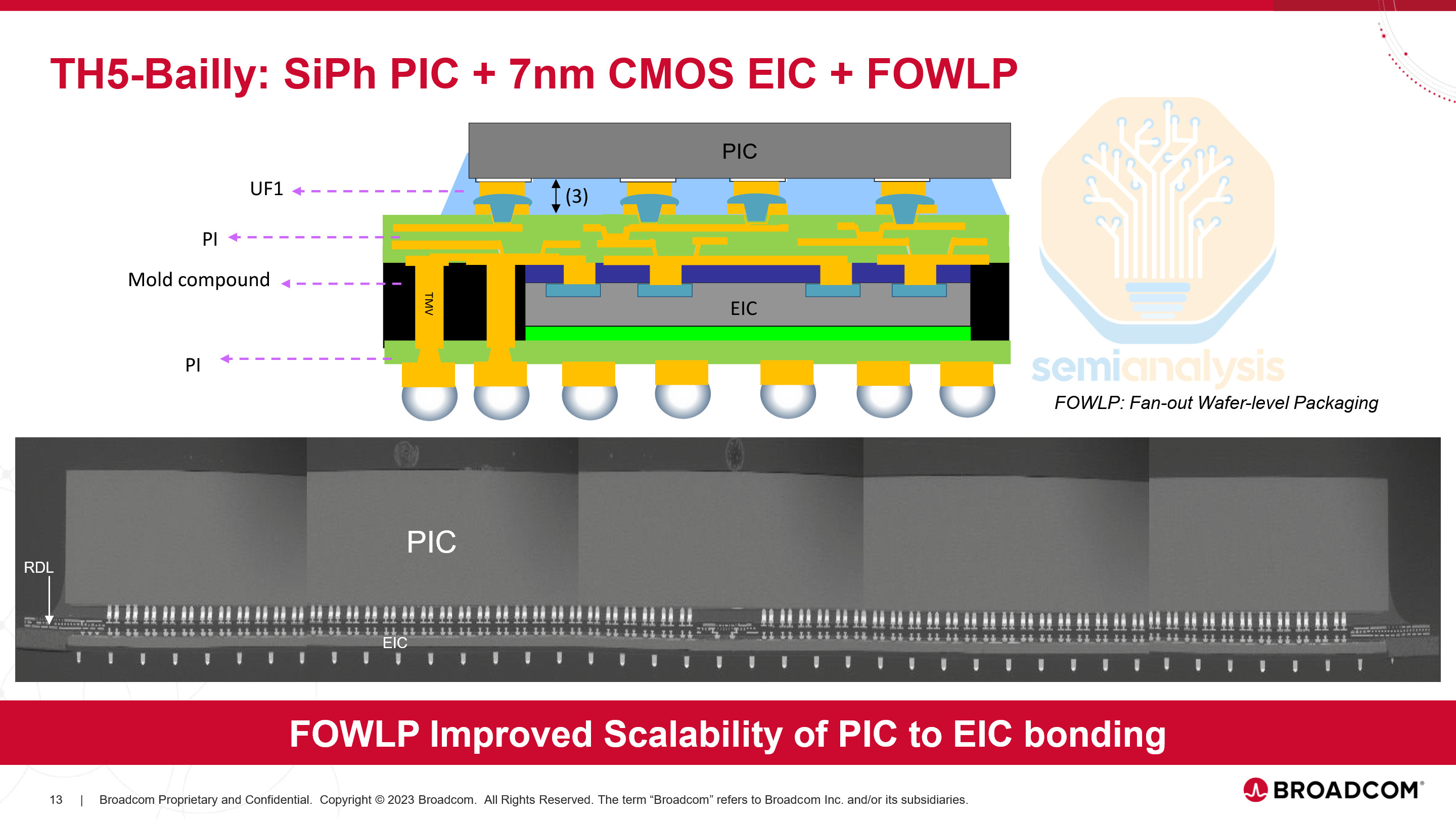
While Nvidia uses COUPE, Broadcom uses a Fan-Out Wafer-Level Packaging approach for this OE. Broadcom will be switching to COUPE in the future, but older generation products like this OE still use other supply chain partners. Here are the promising results from their demonstration:
High-Speed Electrical Interconnects
As multi-die designs become the norm, die-to-die interconnects are a critical bottleneck. Major foundries and chip designers presented approaches to pushing bandwidth density and energy efficiency on both organic substrates and with advanced packaging.
Intel UCIe-S - Paper 8.1
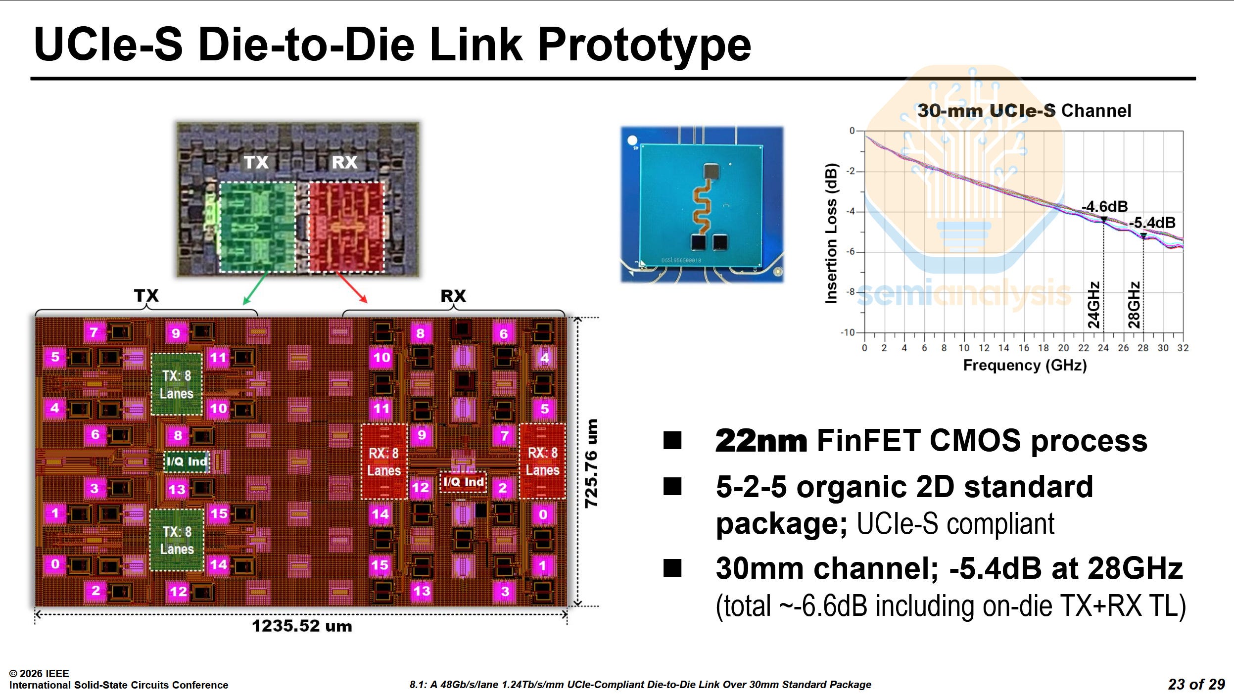
Intel presented their UCIe-S compatible die-to-die (D2D) interface. It can reach up to 48 Gb/s/lane over 16 lanes with UCIe-S and up to 56 Gb/s/lane with a custom protocol. It works on a standard organic package for a distance of up to 30mm. Interestingly, it was manufactured on Intel’s 22nm process.
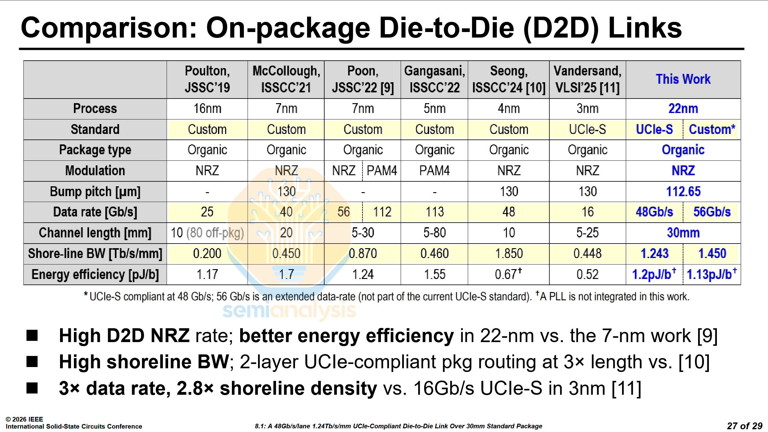
At VLSI 2025, Cadence demonstrated their own UCIe-S die-to-die interconnect on N3E. Despite the node disadvantage, Intel has managed to best Cadence’s interconnect in data rate, channel length and shoreline bandwidth, only losing out in energy efficiency.
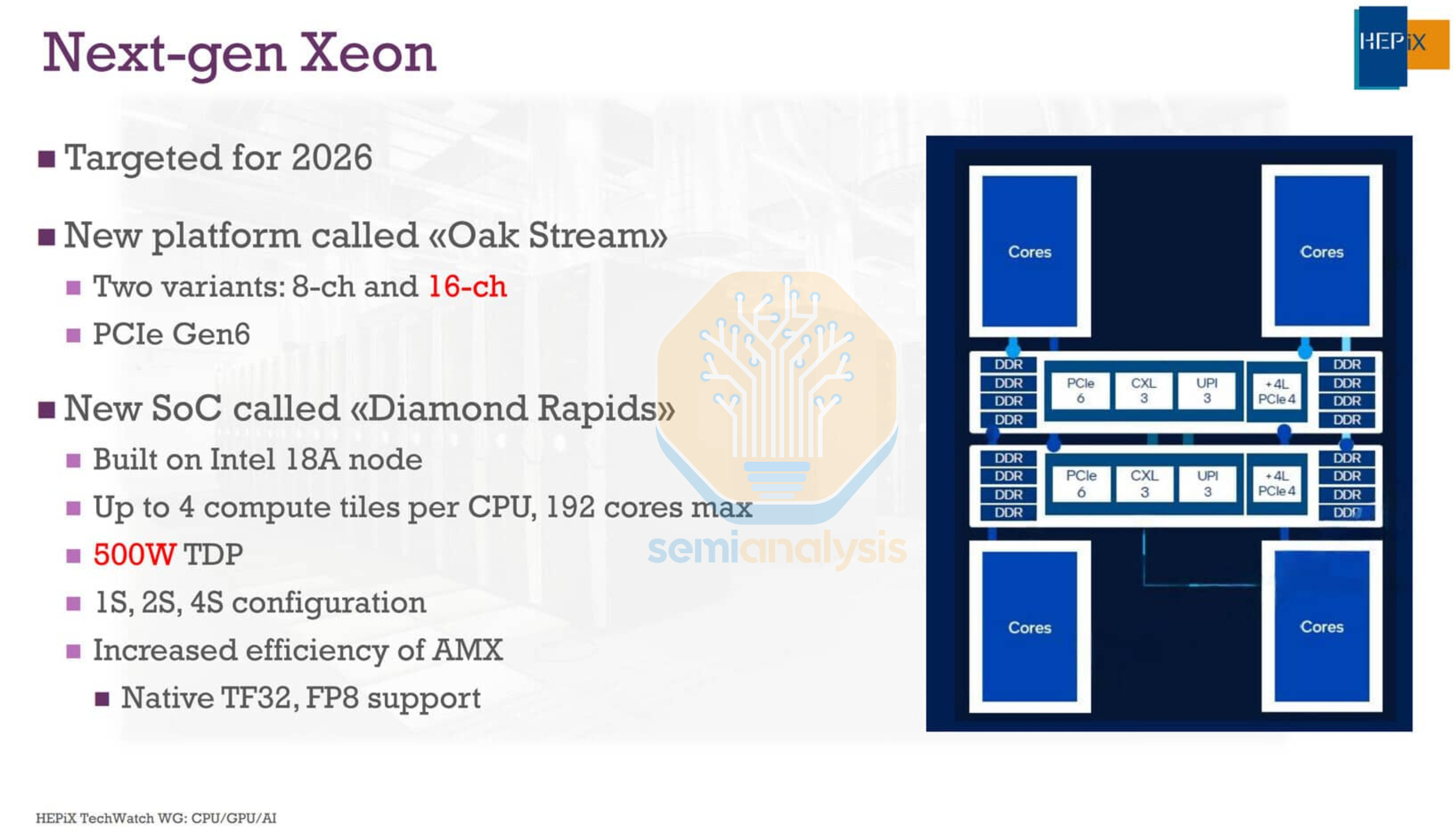
The interconnect presented by Intel is likely to be a prototype of what will be used on their Diamond Rapids Xeon CPUs. Efficiency should be much better when designed on the Intel 3 process compared to this 22nm test chip and could serve to replace the advanced packaging approaches like EMIB on Granite Rapids. As we have covered in our article on the Landscape of Datacenter CPUs, Diamond Rapids consists of two IMH dies, and 4 CBB dies. With the long traces between each CBB die to both IMH dies, we believe this link is a viable candidate to connect the dies over standard package substrate, negating the need for EMIB.
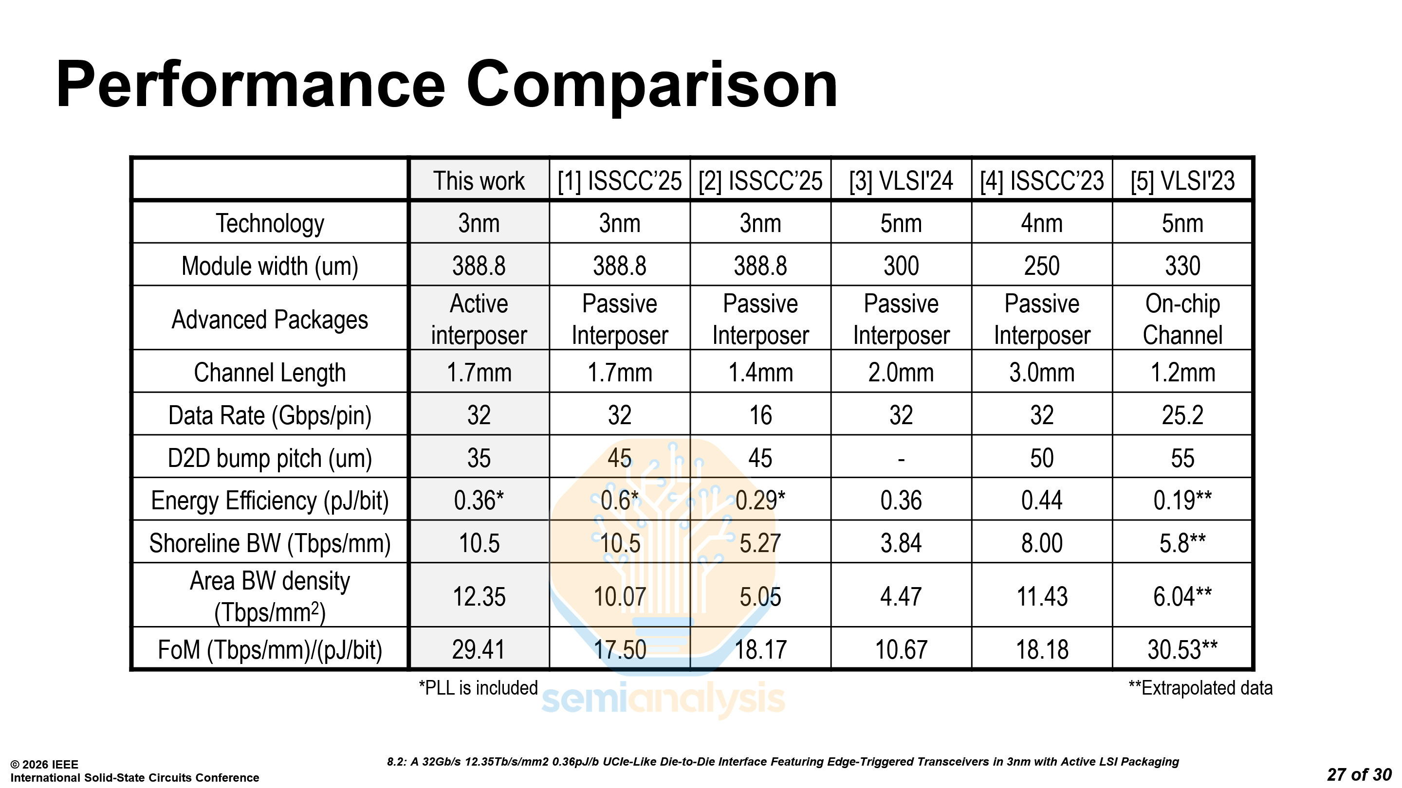
TSMC Active LSI - Paper 8.2
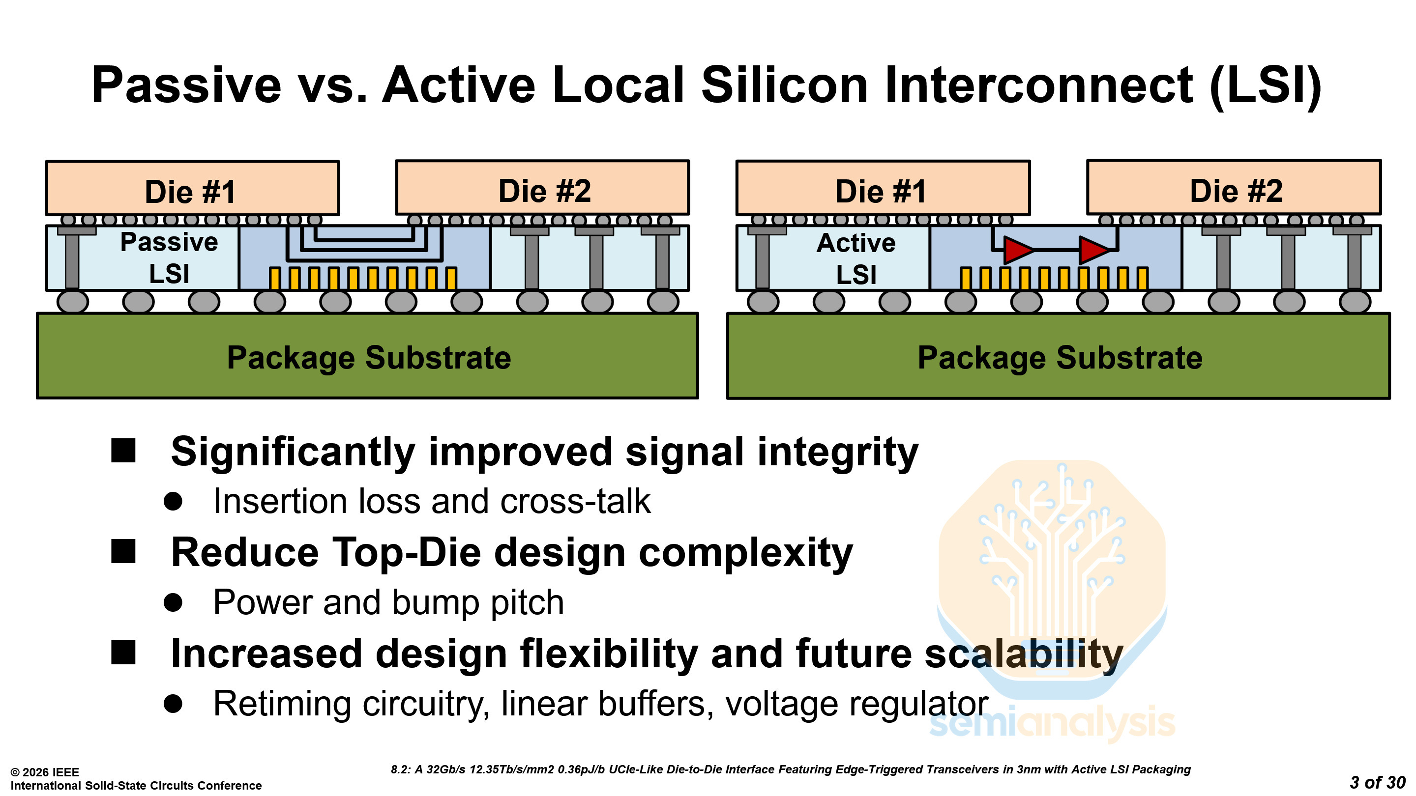
TSMC’s advanced packaging division presented their Active Local Silicon Interconnect (aLSI) solution. As opposed to standard CoWoS-L or EMIB, aLSI improves signal integrity and reduces the complexity of PHYs and SerDes on the top dies.
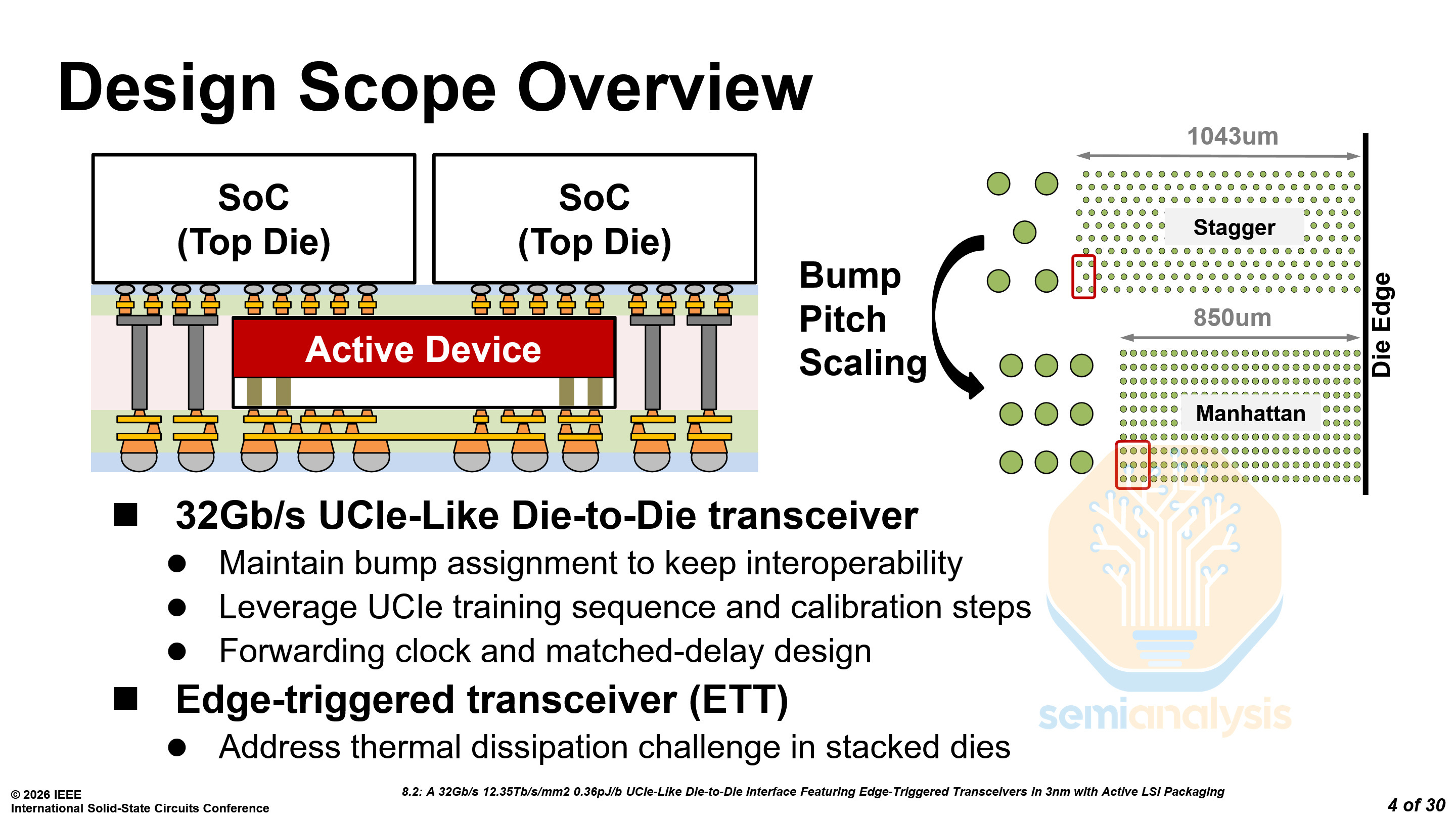
The device that TSMC showed used a 32 Gb/s UCIe-like transceiver. Due to aLSI improving signal integrity, the area of the transceivers could be decreased, and the bump pitch could also be reduced from 45 µm to 38.8 µm. The combination of a tighter pitch and a switch to a Manhattan grid allowed them to reduce the PHY depth from 1043 µm to 850 µm, saving space that designers can reallocate to compute, memory, or IO, or use to shrink the die. The transceiver is only UCIe-like and not true UCIe, as UCIe mandates a hexagonal bump map rather than the Manhattan grid used here.
As designers eke out every bit of die space for next-generation AI accelerators, the switch to aLSI is inevitable.
The ‘active’ part of aLSI comes from replacing the passive long-reach metal channel in the bridge die with active transistors forming an Edge-Triggered Transceiver (ETT) circuit to maintain signal integrity over longer reaches. This also reduces the signal driving requirements of the top die’s Transmit/Receive ports. ETT circuits within the aLSI only add an additional 0.07pJ/b to the energy cost, minimizing thermal concerns from adding active circuits in stacked dies. By moving the signal conditioning circuits to the bridge die, PHY area on the top die TX/RX can be reduced by using smaller pre-drivers and clock buffers and remove the need for signal amplification on the receive end.
The ETT integrates a driver, an AC-coupling capacitor (Cac), an amplifier with both negative and positive feedback, and an output stage. Running the signal through the Cac introduces peaks in the signal transition edges, which is then picked up by the dual-loop amplifier, hence the edge-triggered nomenclature. The amplifier leverages both positive and negative feedback loops to stabilize the voltage level. In this design, Cac is set to be 180 fF for a 1.7 mm channel length, with 2kΩ resistance on die A and 3kΩ on die B respectively.
These aLSI bridges can also integrate embedded deep trench capacitors (eDTC) along the front-end to improve power delivery to the PHY and D2D controllers. Instead of compromising the power grid by having a bridge die in the way, aLSI with eDTC improves both the power and signal routing along the D2D interfaces.
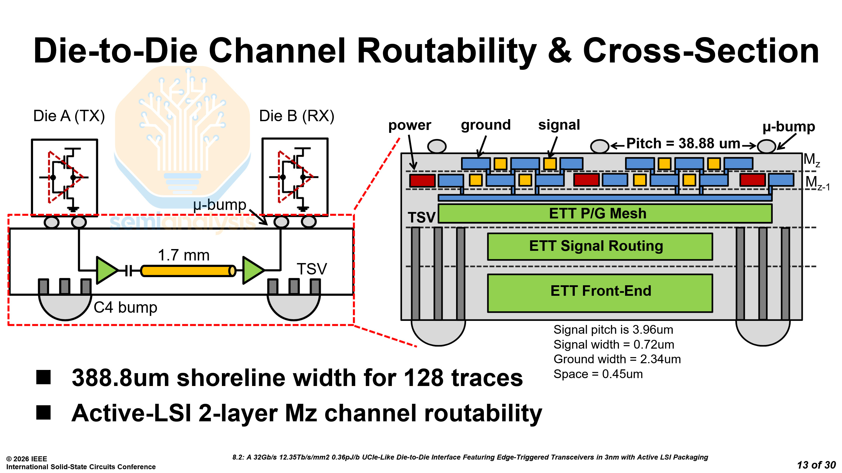
Only 388 µm of shoreline is required for 64 TX and 64 RX data lanes, coming out to a total area of 0.330 mm². Only the top 2 metal layers are required for routing the signals. The remaining metal layers can be used for the front-end circuitry.
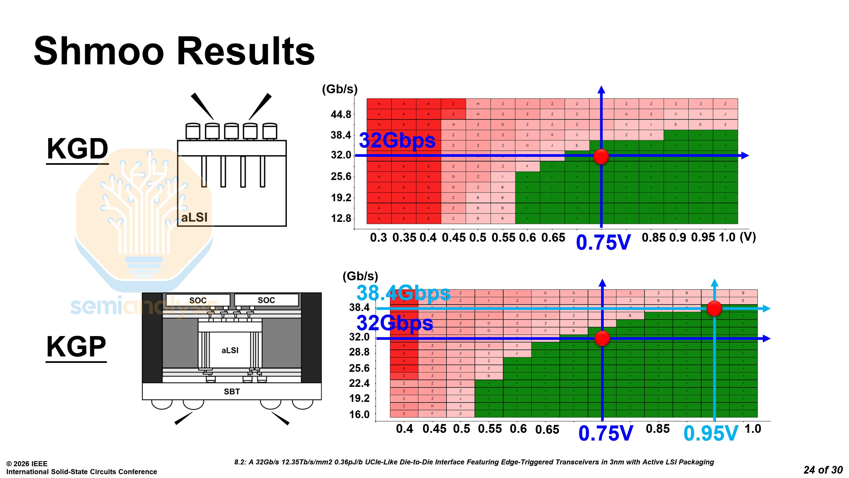
TSMC explained how the Active LSI can be tested at multiple stages. The first is Known Good Die (KGD) with just the LSI for die validation. Next is Known Good Stack (KGS) with the SoCs connected by the LSI for stack functionality. Lastly is Known Good Package (KGP) with the full assembly to comprehensively verify functionality, performance and reliability.
They showed shmoo plots at the KGD and KGP stages, both showing the interconnect hitting 32 Gb/s at 0.75V and 38.4 Gb/s at 0.95V.
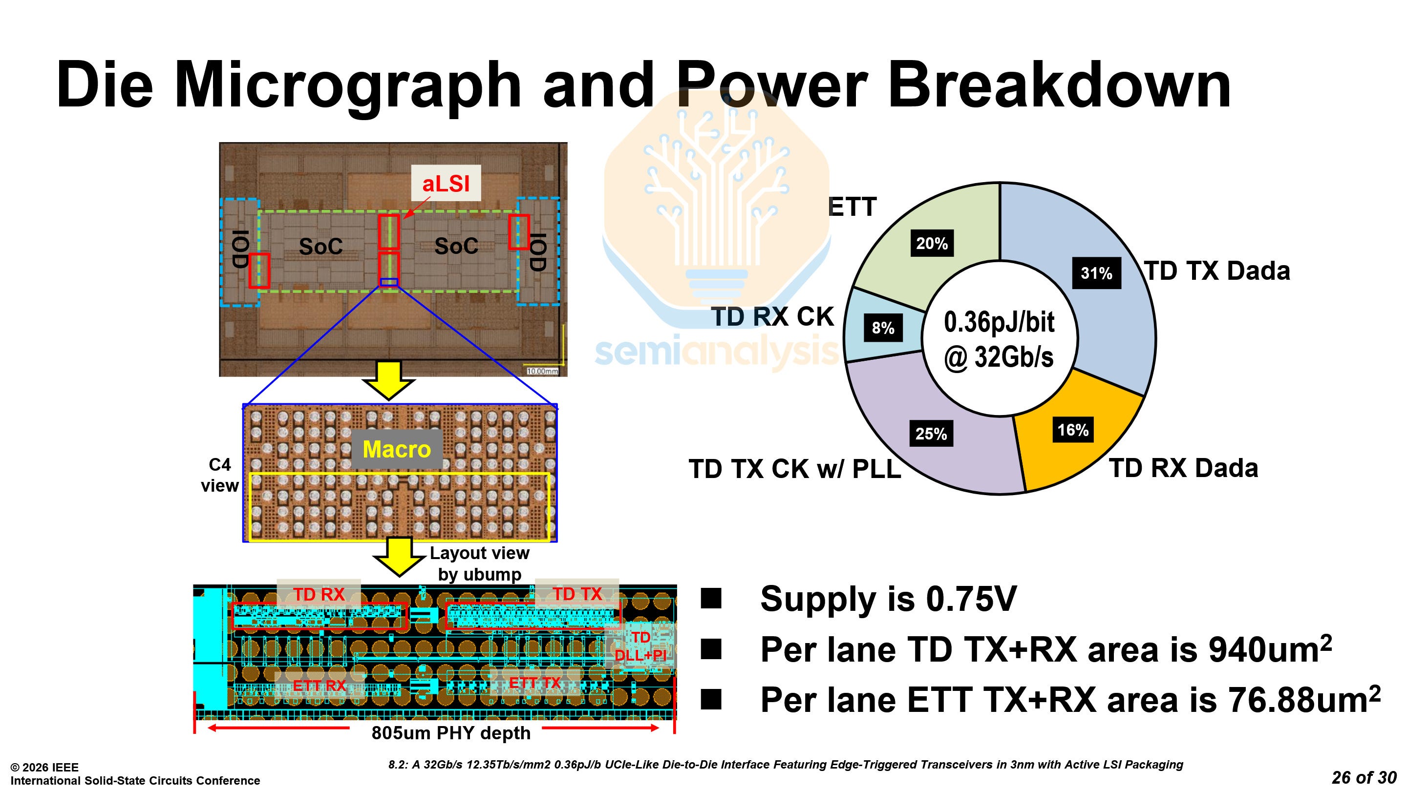
The package reveals two SoC dies and two IO dies. Interestingly, the test vehicle appears to match AMD’s MI450 GPU’s design, with 2 base dies connected to each other, 12 HBM4 stacks and 2 IO dies with Active LSI. Instead of each individual HBM4 stack having its own Active LSI, two HBM4 stacks share one.
As for the power, the total is only 0.36 pJ/b at 0.75V, with only 0.07 pJ/b being used by the ETT in the Active LSI. Below is a comparison with other D2D solutions.
Microsoft D2D Interconnect - Paper 8.3
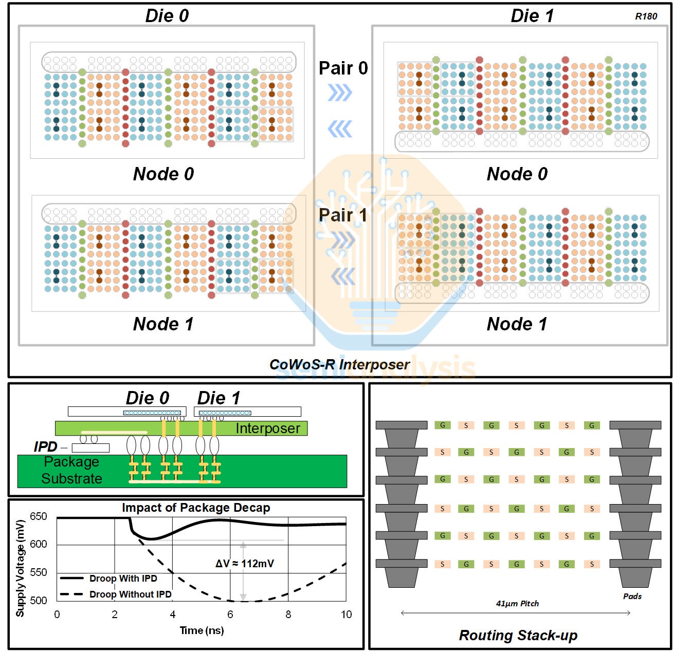
Microsoft also detailed their die-to-die (D2D) interconnect. Their test vehicle includes two dies and two pairs of D2D nodes for interconnection. A full mock-up of the power delivery network and routing were included to mimic clock gating and crosstalk.
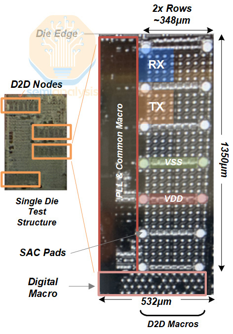
The interconnect on their test die occupied 532 µm of shoreline and had a depth of 1350 µm. The test vehicle was fabricated on TSMC’s N3P node, and the interconnect was tested at two data rates, 20 Gb/s at 0.65V, and 24 Gb/s at 0.75V.
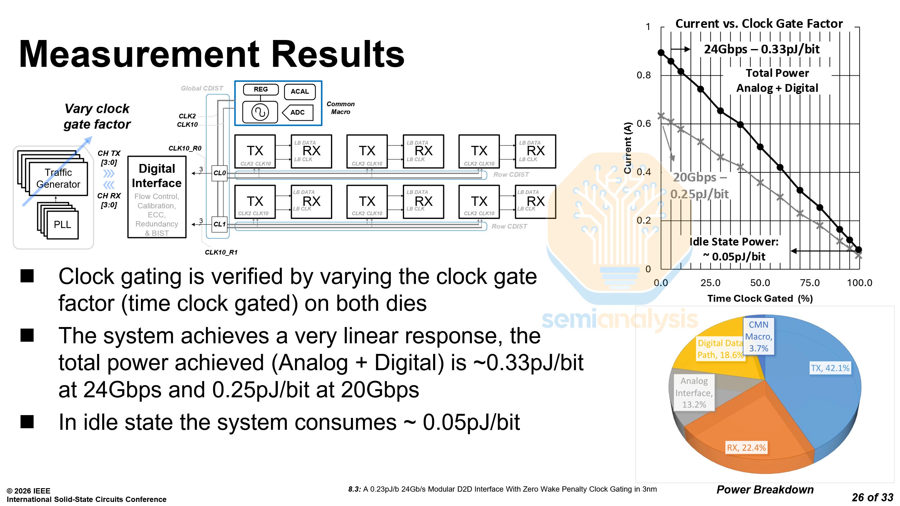
Microsoft reported two power consumption figures, one with both analog and digital system power, and one with only analog power. The latter is what most die-to-die interconnects report. At 24 Gb/s, the system power is 0.33 pJ/b and the analog power is 0.226 pJ/b, while at 20 Gb/s, the system power is 0.25 pJ/b and the analog power is 0.17 pJ/b. The power at idle state is 0.05 pJ/b.
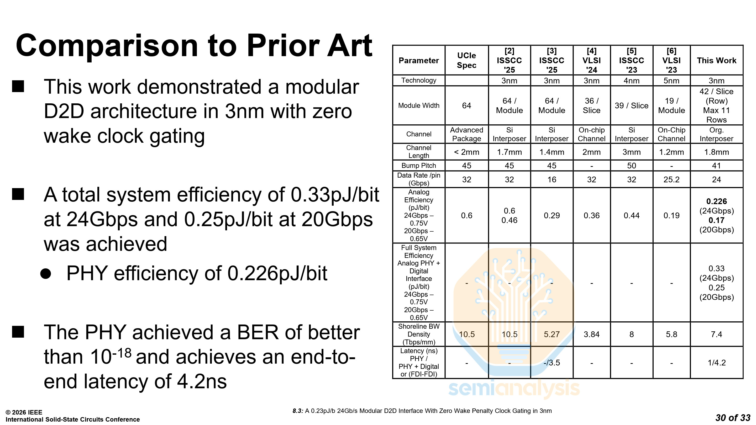
Microsoft also compared their interconnect to the same prior research as TSMC did for their Active LSI.
As we explained in a previous article, Microsoft’s Cobalt 200 CPU features two compute chiplets connected by a custom high-bandwidth interconnect. We believe that this presentation details that exact interconnect.
Processors
From small mobile CPUs to large AI accelerators, ISSCC featured first-time architectural breakdowns from MediaTek, Intel, AMD, Rebellions, and Microsoft. Many even included die shots.
MediaTek Dimensity 9500 - Paper 10.2
Every year, MediaTek presents a different aspect of their flagship mobile CPUs. This year is no different, and the focus of this year’s mobile CPU presentation was on boosting and thermal management.
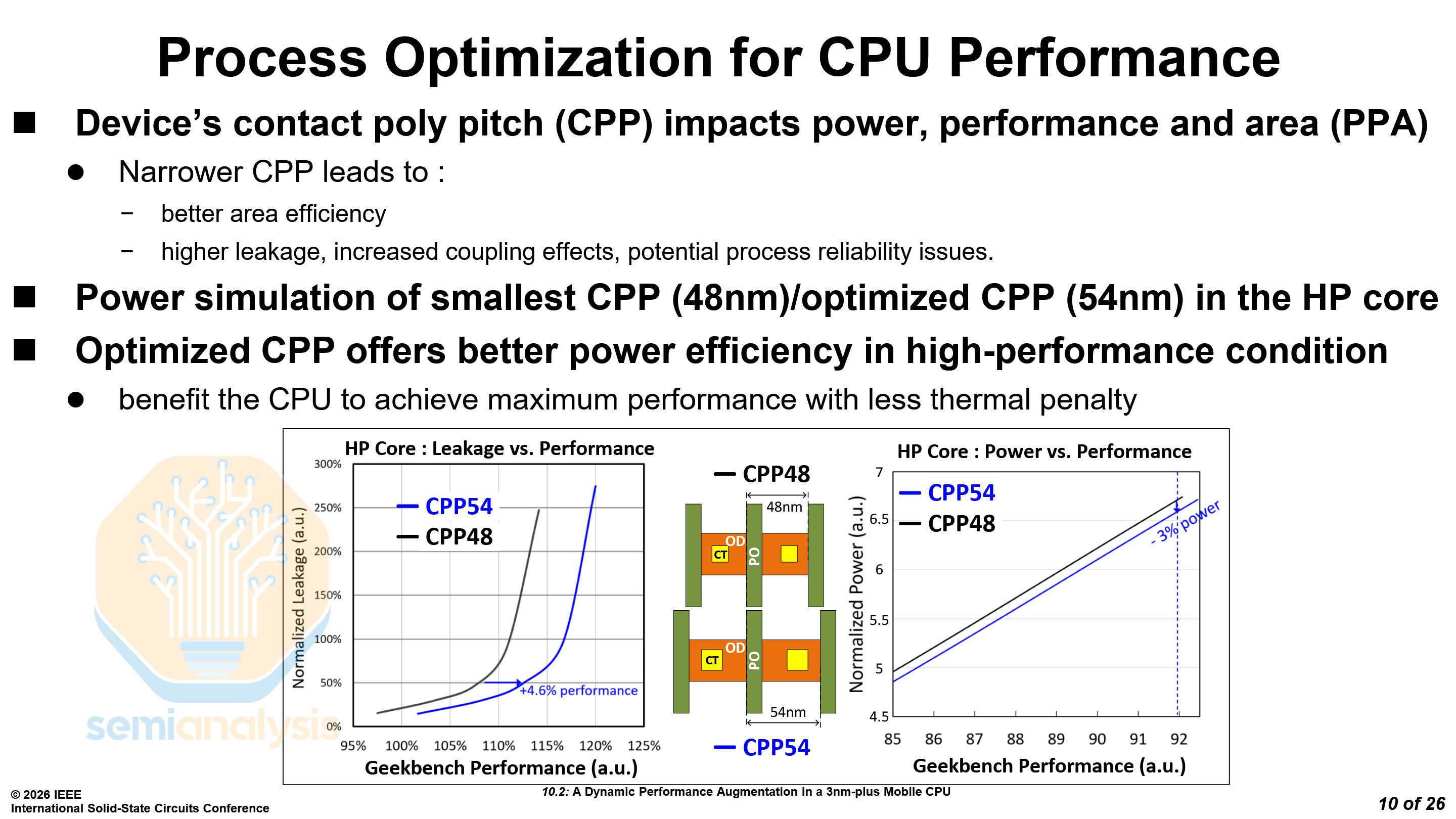
TSMC offers two different Contacted Gate Pitch (CGP) options for N3E and N3P, 48nm and 54nm. Across most chips, the narrower CGP of 48nm has been used, as it leads to smaller cell sizes and a greater die shrink. However, it also faces problems with leakage, routing and manufacturing due to the smaller critical dimensions.
MediaTek used the larger 54nm CGP on their Dimensity 9500’s C1 Ultra high-performance cores, for the improved power efficiency. This allowed them to reach higher performance with less thermal penalty, with 4.6% more performance at iso-leakage or 3% less power at iso-performance.
The rest of MediaTek’s paper focuses on dynamic performance optimization by utilizing unused aging budget and reducing thermal overshoots. In total, they were able to increase boost clocks from 4.21 GHz to 4.4 GHz. If these optimizations sound interesting to you, we recommend you check out the paper, 10.2 A Dynamic Performance Augmentation in a 3nm-Plus Mobile CPU.
Intel 18A-on-Intel 3 Hybrid Bonding - Paper 10.6
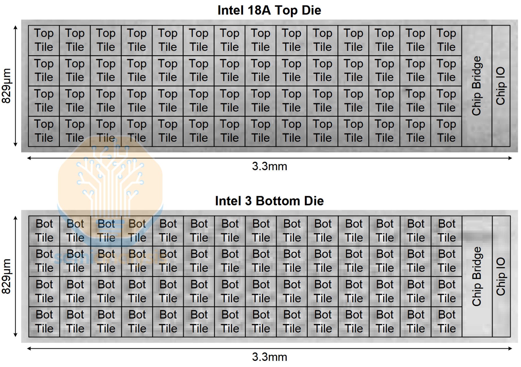
Intel disclosed their first hybrid bonded chip, the M3DProc. It consists of an Intel 3 bottom die, and an 18A top die. Each die contains 56 mesh tiles, cores and DNN accelerator tiles, respectively. The two dies are bonded together with Foveros Direct, hybrid bonding at a 9μm pitch.
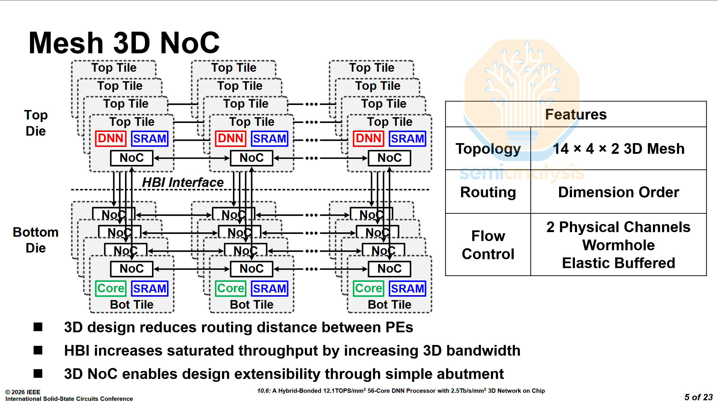
The mesh tiles are arranged in a 14×4×2 3D mesh, with SRAM being shared across both dies.
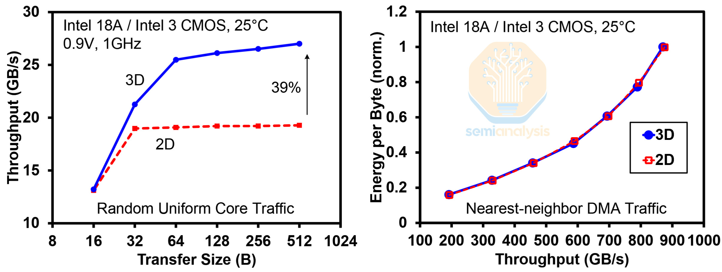
Intel found that the 3D mesh reduces latency and increases throughput by almost 40%. They also tested the energy efficiency of transferring data, with 2D being within the 56 mesh tiles of the bottom die, and 3D being 28 adjacent mesh tiles across both dies. The results show that the Hybrid Bonding Interconnect (HBI) had a negligible impact on efficiency.
Each tile has 552 pads, with just under half used for data, and just under a quarter used for power.
In terms of packaging, M3DProc is similar to Clearwater Forest (CWF). CWF has Intel 3 base dies, connected to 18A compute dies via 9μm Foveros Direct.
The M3DProc achieves 875 GB/s 3D bandwidth, while each CWF compute die only achieves 210 GB/s. This chip’s 3D NoC has a significantly higher bandwidth density. CWF uses Foveros Direct to disaggregate the CPU core cluster’s L2 cache from the base L3 with 6 clusters per top die at 35GB/s each for 210GB/s per top die. M3DProc’s 875GB/s 3D bandwidth is aggregated over 56 vertical tile connections, or 15.6GB/s each over a far smaller area.
AMD MI355X - Paper 2.1
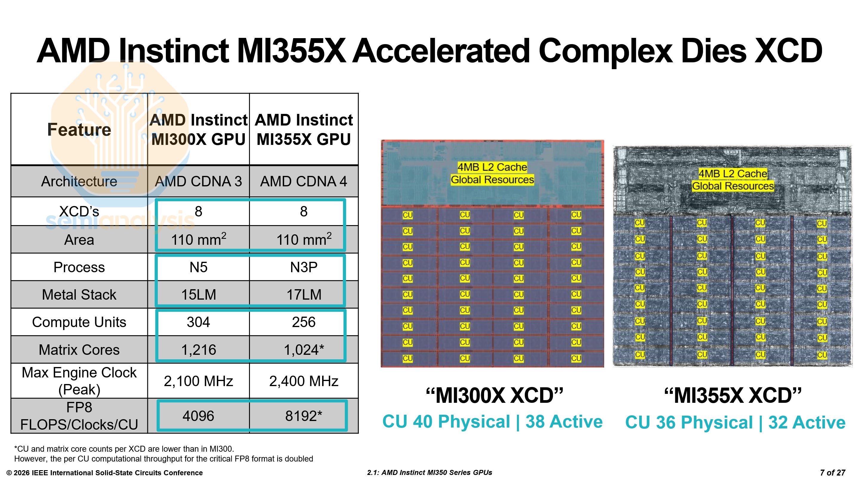
AMD presented on their MI355X GPUs. In conference presentations, AMD usually rehashes prior announcements while only introducing one or two new pieces of information. This paper was much better in that regard, explaining how the MI355X XCD and IOD were improved as compared to the MI300X.
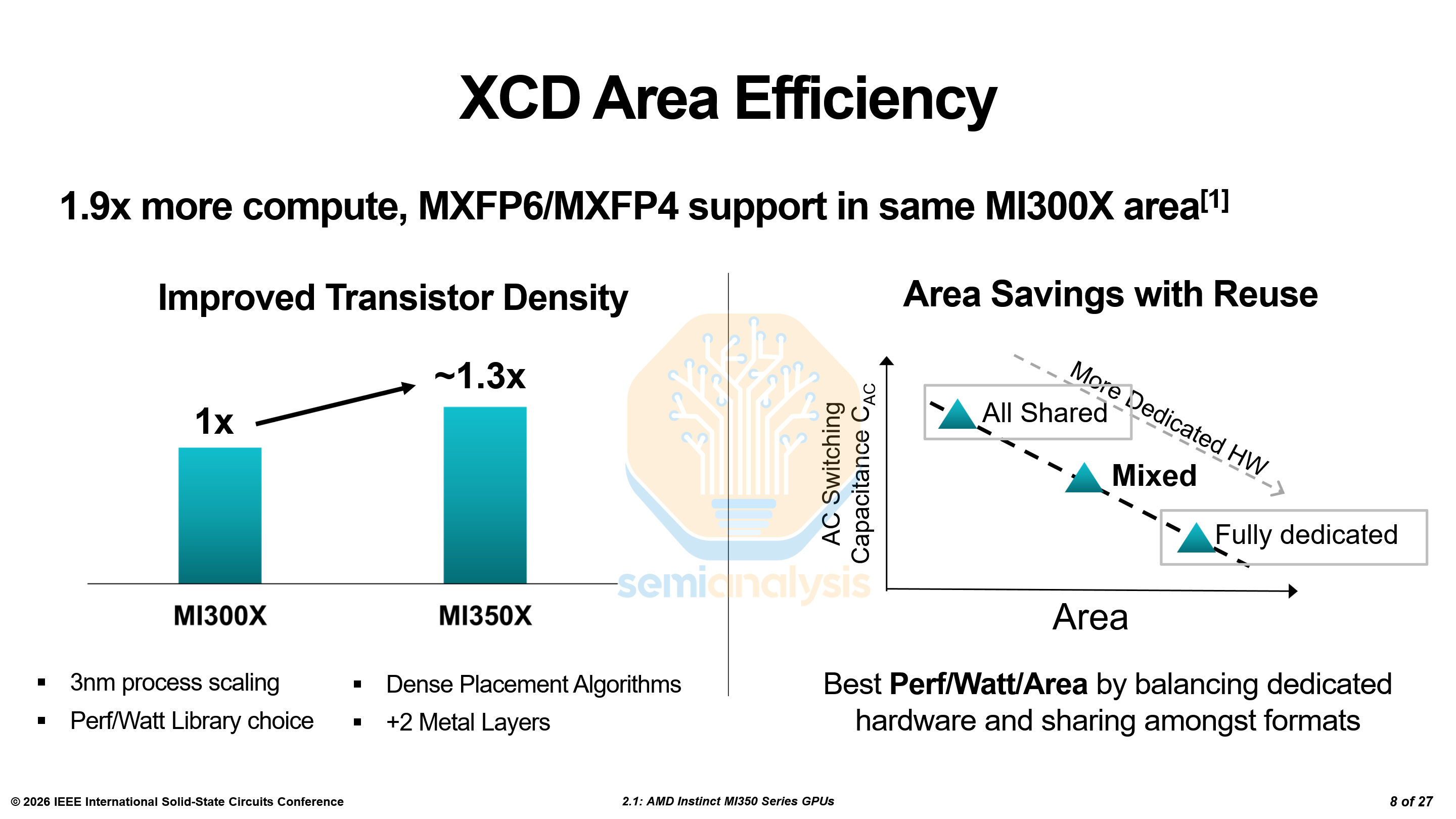
AMD detailed how they doubled the matrix throughput per CU while keeping the total area the same and the number of CUs largely similar. First, of course, was the move from N5 to N3P; this provided the bulk of the transistor density improvement. The additional two metal layers provided by N3P allowed for improved routing and thus, higher cell utilization. AMD designed their own standard cells, as they have with N5 before, to optimize the node for their HPC use case.
They also used denser placement algorithms, similar to how the Zen 4c cores used in EPYC Bergamo CPUs are much smaller than the Zen 4 cores used in EPYC Genoa CPUs.
There are two approaches when performing the same calculations with many different data formats like FP16, FP8, MXFP4, etc. The first is using shared hardware, where every format goes through the same circuits. However, this comes with a power cost as there is little optimization for each format. The second option is each data format using an entirely different set of circuits for calculations. However, this takes up a lot of additional space. Of course, the optimal approach is somewhere in the middle. This optimization was an important focus for AMD.
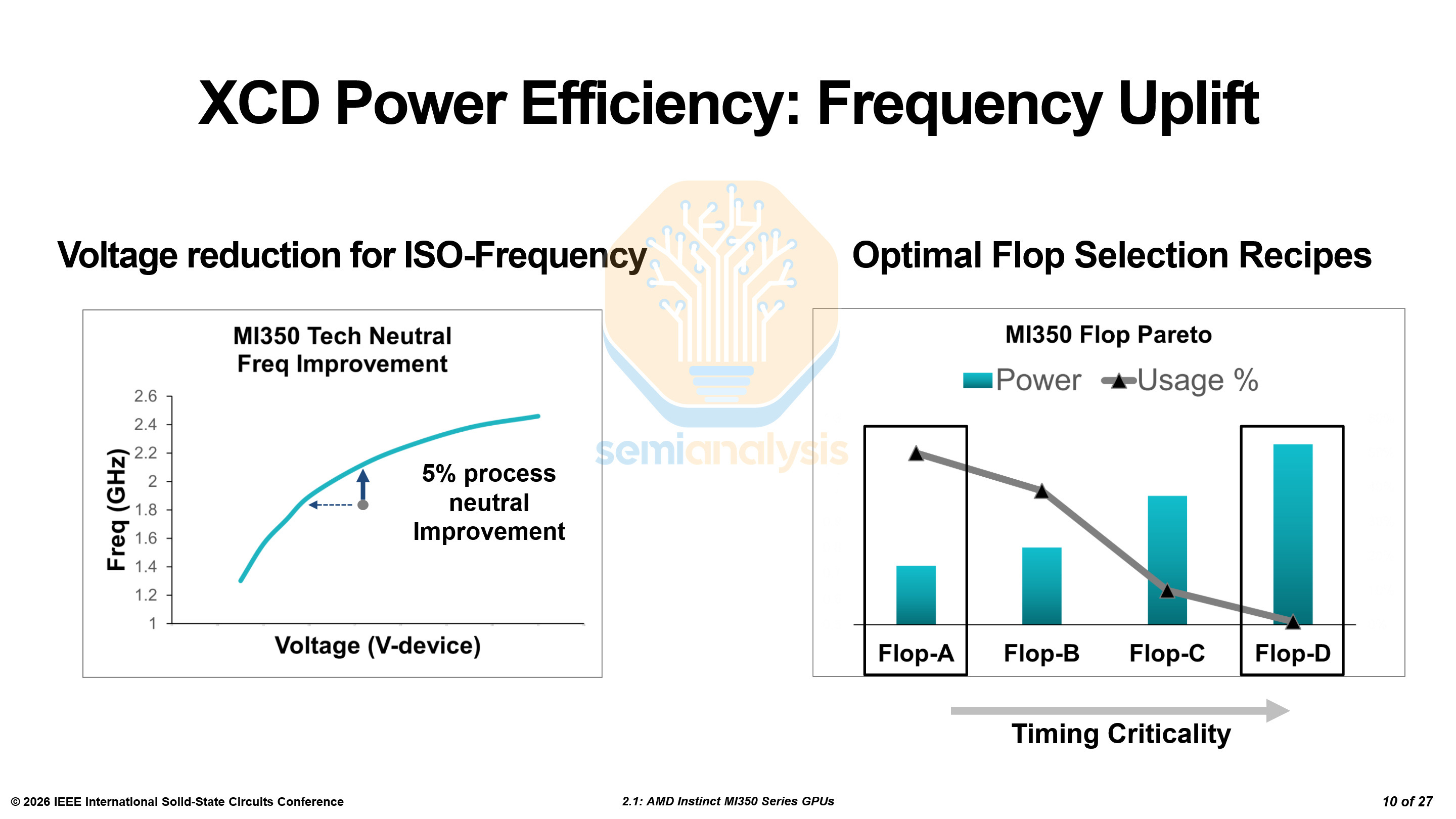
As the next node with improved transistors, N3P provides performance improvements by itself. Nevertheless, AMD was able to improve frequency iso-power by 5% before process node improvements. They also designed multiple flip-flop variants with varying power and performance characteristics deployed across different areas of the chip depending on usage and architectural requirements.
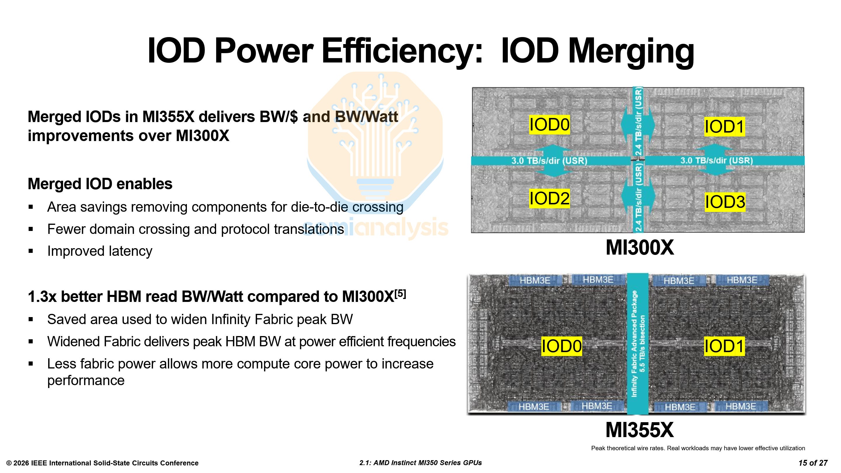
MI300X featured 4 IO Dies. MI355X cuts that down to two. By doing this, AMD saves area on die-to-die interconnects. A larger monolithic die improves latency and reduces SerDes and translations. Moreover, the efficiency of the HBM was also improved by increasing the interconnect width. The saved power could be reallocated to the compute dies to increase performance.
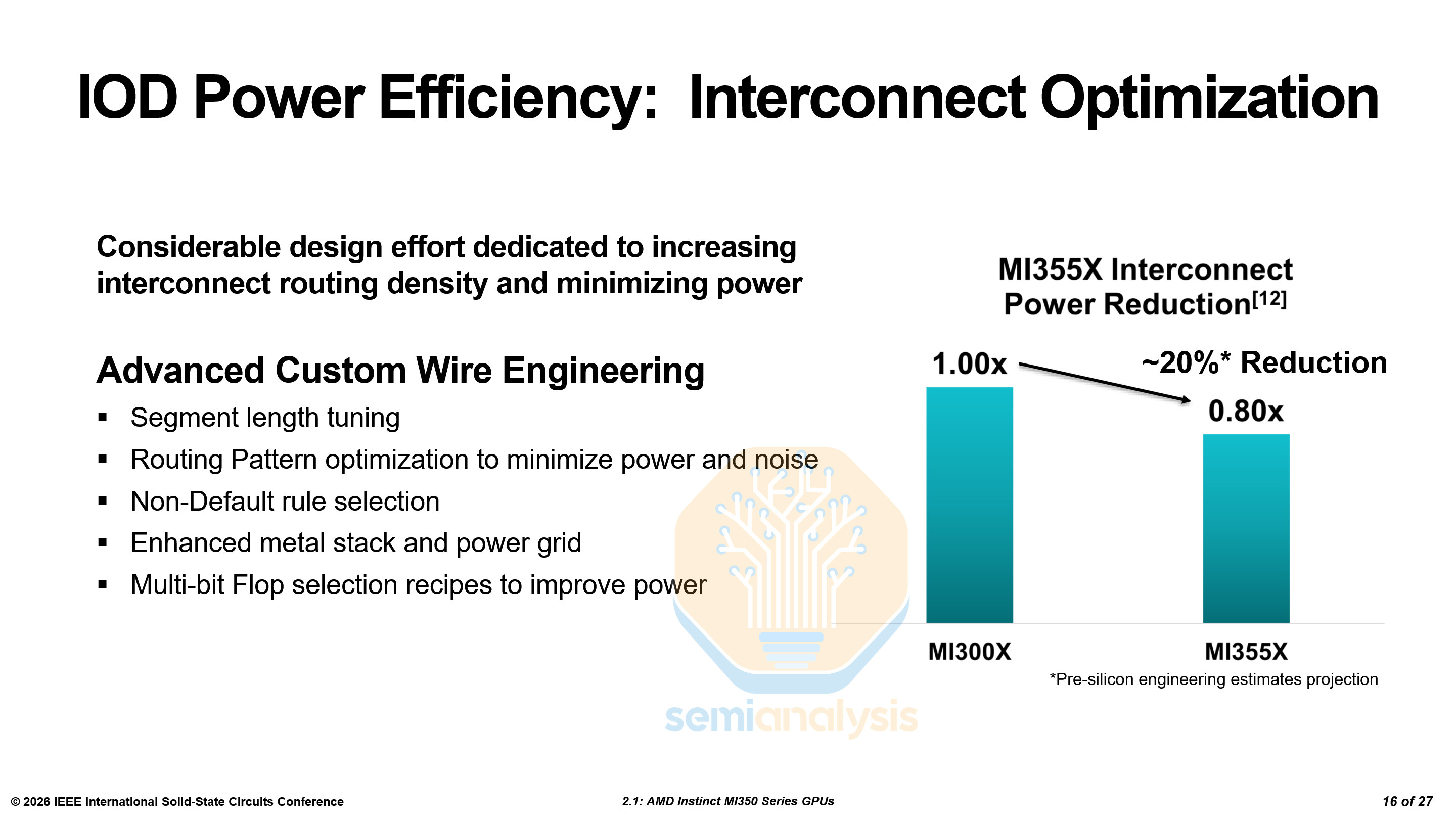
As a large die with many routing options between any two areas on the chip, AMD had to do a lot of work to optimize the wires and interconnects. Through custom engineering of the wires, AMD was able to reduce the interconnect power consumption by ~20%.
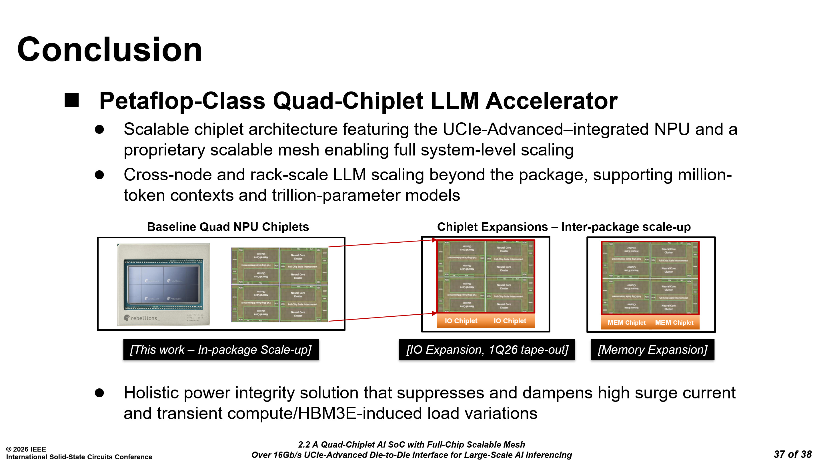
Rebellions Rebel100 - Paper 2.2
Rebellions is a South Korean startup working on AI accelerators. At ISSCC, they published the first architectural breakdown of their new accelerator, the Rebel100. Unlike other accelerators, which are generally manufactured at TSMC, Rebellions chose Samsung Foundry’s SF4X node. With Nvidia, AMD, Broadcom and others hogging most of TSMC’s capacity, this allows them more flexibility.
At Hot Chips 2025, Rebellions demonstrated the chip running Llama 3.3 70B. The specs have remained the same between Hot Chips and ISSCC. One key point to note is the use of Samsung’s I-CubeS interposer technology. While the Hot Chips slide mentions the usage of TSMC’s CoWoS-S, we have clarified that this was a mistake on the slide, and that it has always been I-CubeS.
We have recently mentioned that CoWoS-S capacity constraints have been easing. That said, Samsung may have offered steep discounts to bundle I-CubeS advanced packaging with their front-end process — sparing the startup from having to find and validate a separate advanced packaging supplier. Samsung may have also conditioned the availability of their HBM on using I-CubeS.
I-CubeS has not seen adoption among any of the leading AI accelerators, and this could be Samsung’s attempt to break into the market. There are only 5 confirmed users of I-CubeS: eSilicon, Baidu, Nvidia, Rebellions and Preferred Networks.
The first is a networking ASIC by eSilicon on Samsung’s 14LPP with HBM2. Baidu’s Kunlun1 accelerator is similar, using Samsung’s 14LPP process and 2 HBM2 stacks. When the CoWoS-S capacity was very tight back in 2023, Nvidia outsourced a small amount of H200 production to I-CubeS. Then, there is the Rebel100 and lastly, a planned accelerator from Preferred Networks on the SF2 process.
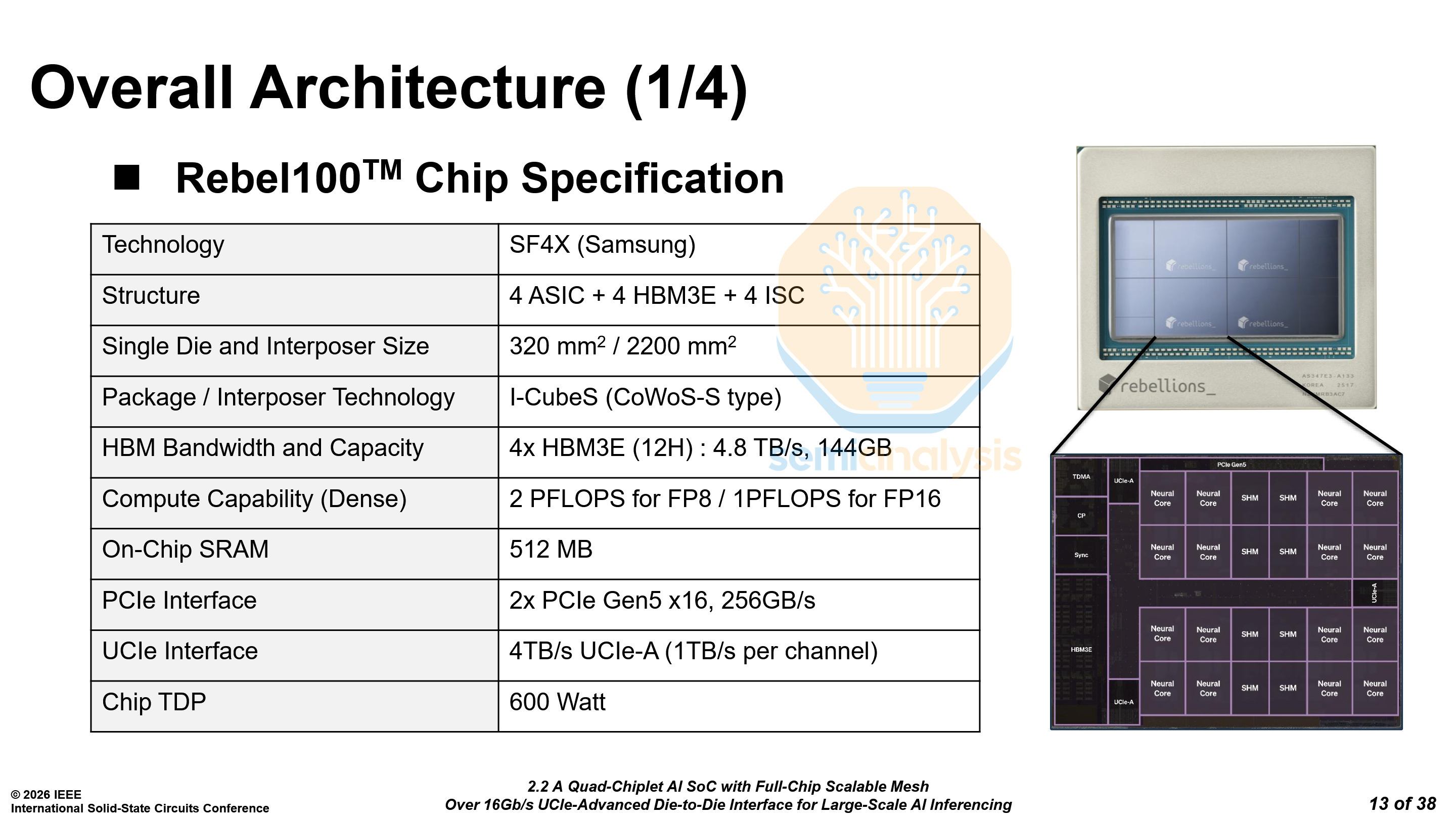
The Rebel100 uses 4 compute dies and 4 HBM3E stacks. Each die has 3 UCIe-A interfaces. However, only two are used on each die, clocked at 16 Gb/s.
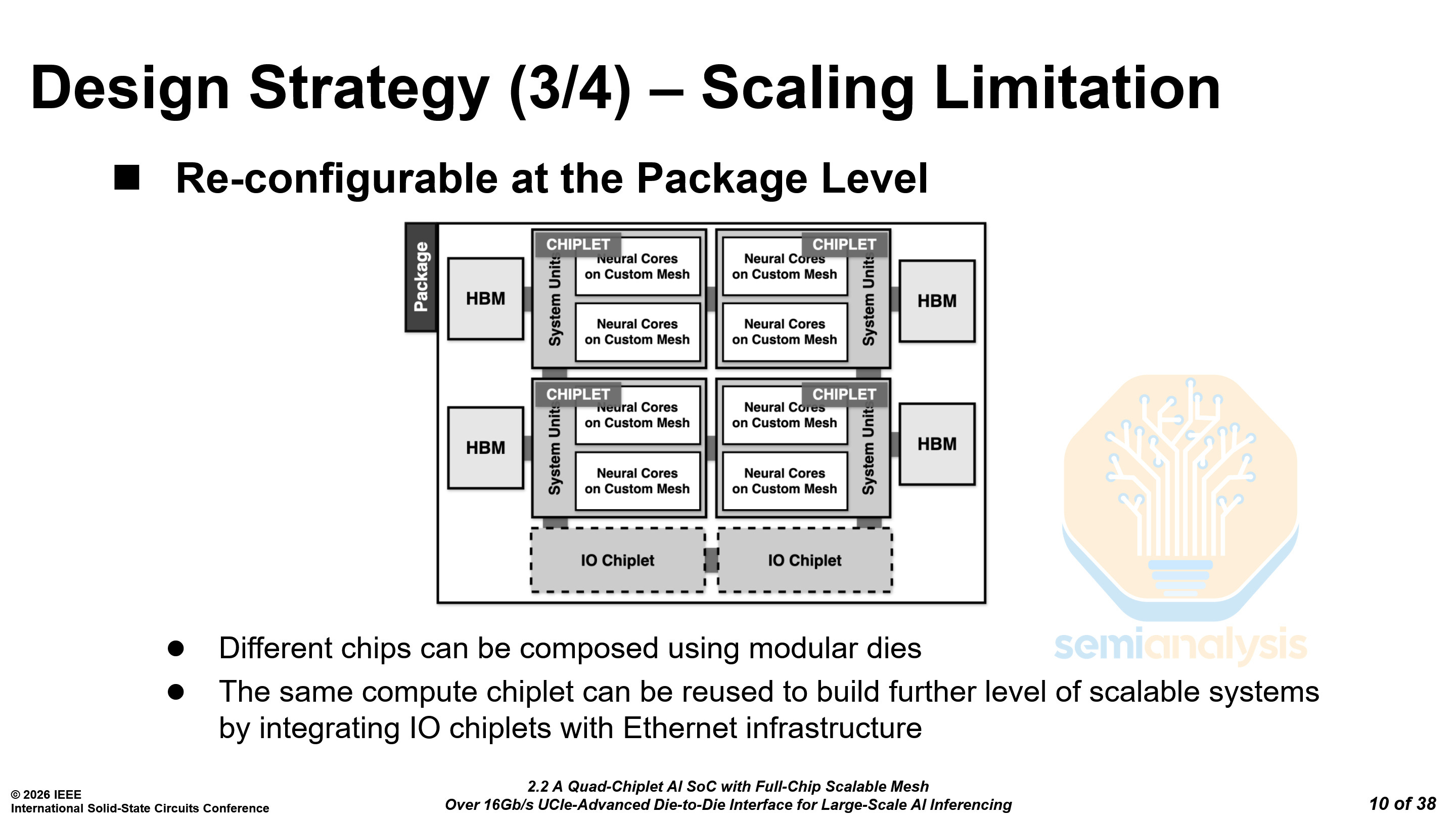
Rebellions claims that the design is reconfigurable at the package level, where additional IO or memory chiplets can be added to integrate with Ethernet for scale-up. This is where the remaining UCIe-A interface would be used.
Rebellions stated that the IO chiplets would be taped out by 1Q2026. There was no provided timeline for the memory chiplets.
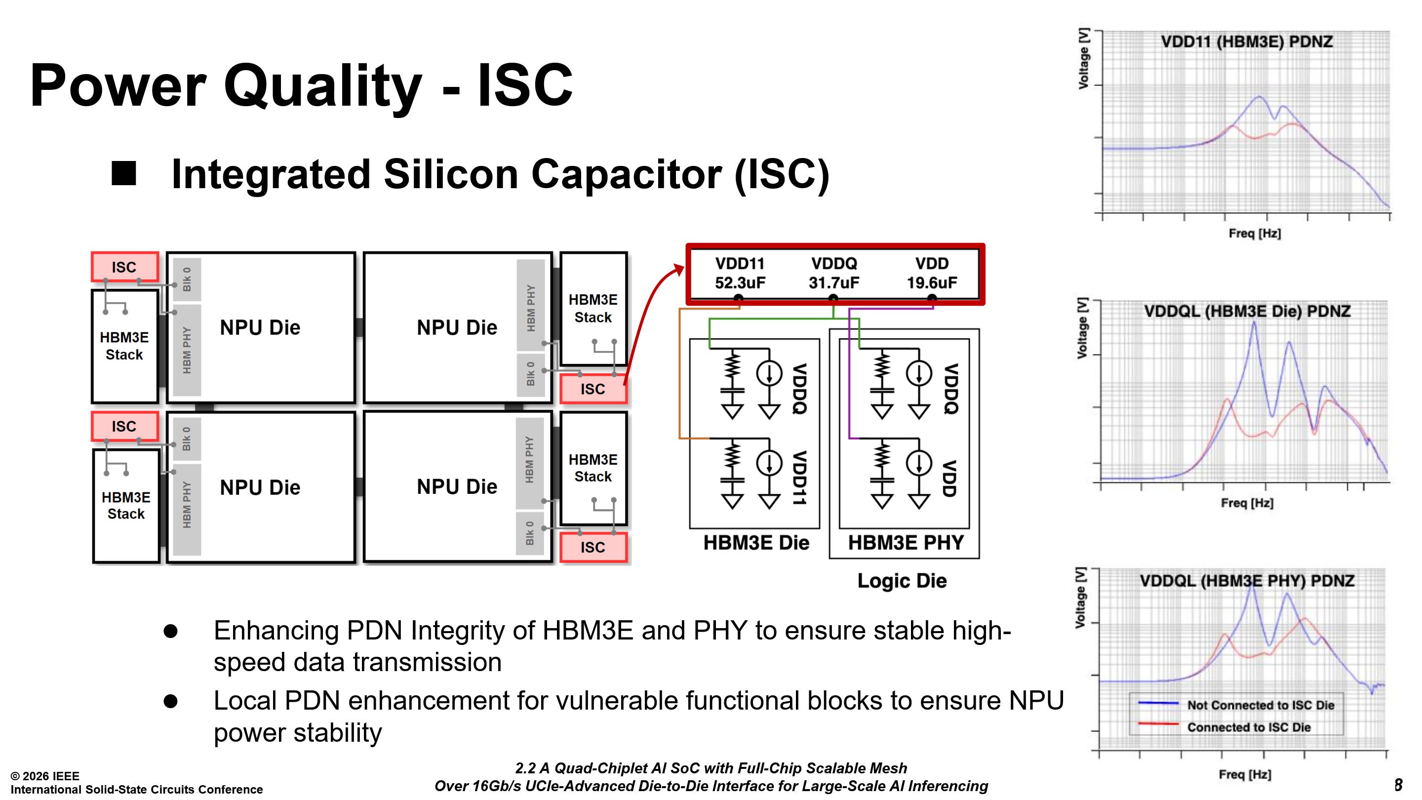
They have also integrated silicon capacitors beside each HBM3E stack to improve power quality for HBM3E and critical control blocks.
Microsoft Maia 200 - Paper 17.4
Microsoft detailed their Maia 200 AI accelerator. The paper was less of a research paper and more of a white paper, with only a single image, a spec sheet comparing it to the Maia 100. Makes sense given a lot of Maia 200 claims are dubious such as the flops/mm^2 and flops/w.
While the Maia 100 was designed in a pre-GPT era, Maia 200 was designed for the current age of models and specifically inference. Earlier this year, Maia 200 nodes were made generally available on Azure.
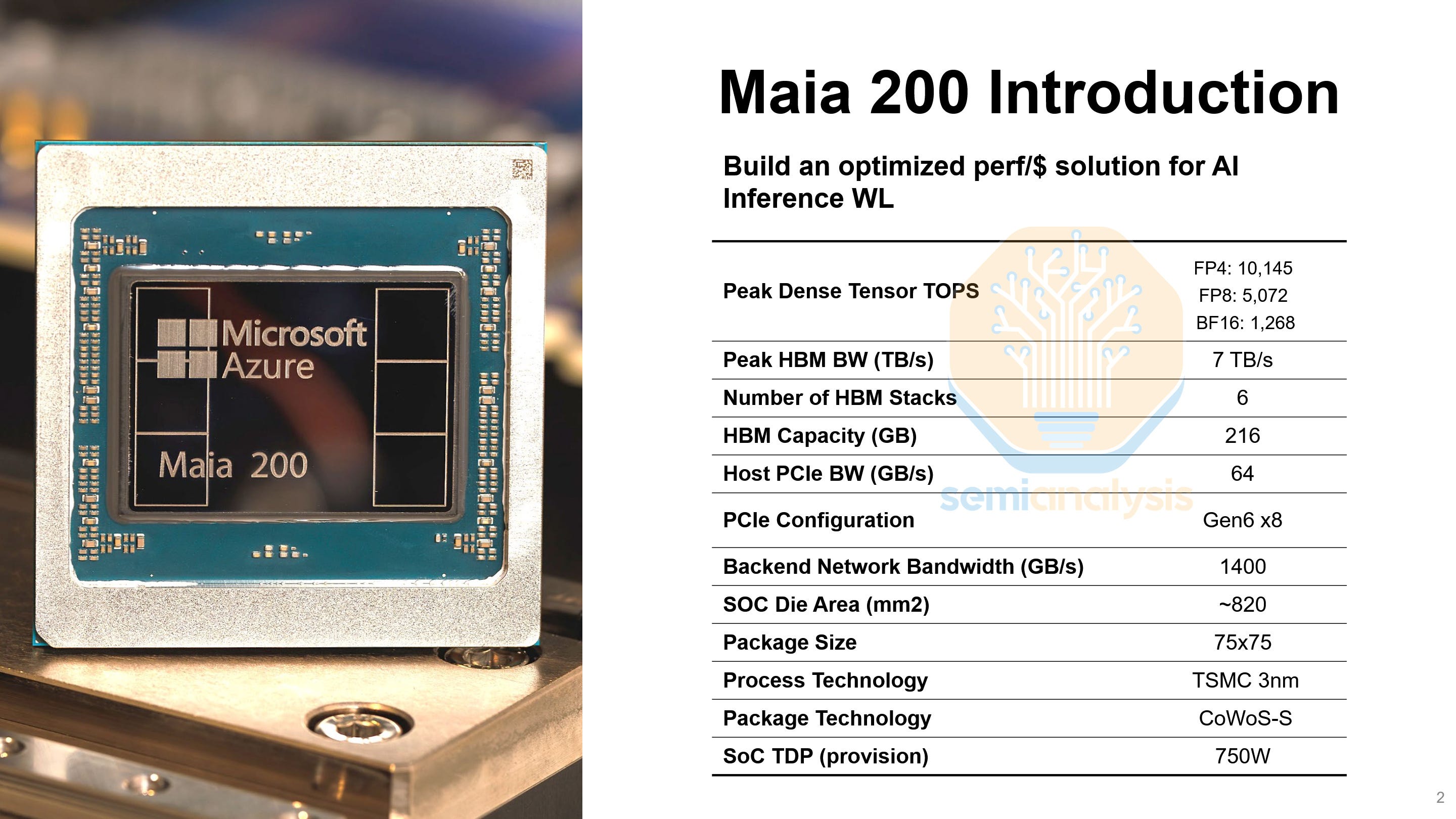
Maia 200 is the last holdout of reticle-scale monolithic designs. Every major HBM-equipped training and inference accelerator has moved on to multi-chip designs with 2, 4, or even 8 compute dies per package. Every single mm² of the die has been hyper-optimized for one purpose. Unlike with an Nvidia or AMD GPU, there is no legacy hardware for media or vector operations. Microsoft has pushed the reticle-scale monolithic approach to its limit on TSMC’s N3P process, packing in over 10 PFLOPs of FP4 compute, 6 HBM3E stacks, and 28× 400 Gb/s full-duplex D2D links.
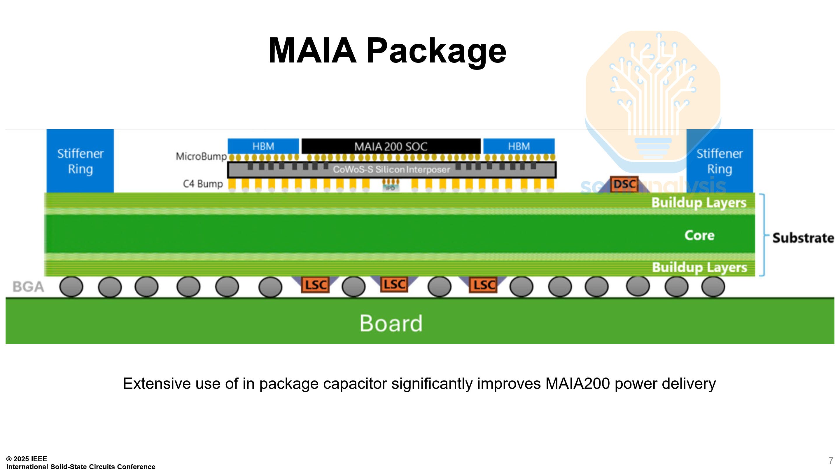
On the package-level, Maia 200 is very standard, mimicking the H100. A CoWoS-S interposer, with 1 main die, and 6 HBM3E stacks.
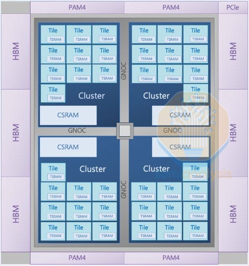
The long sides of the chip are covered in 3 HBM3E PHYs each, while the short sides each have 14 of the 28 lanes of 400 Gb/s D2D links. In the center, there is 272 MB of SRAM, with 80 MB of TSRAM (L1) and 192 MB of CSRAM (L2).
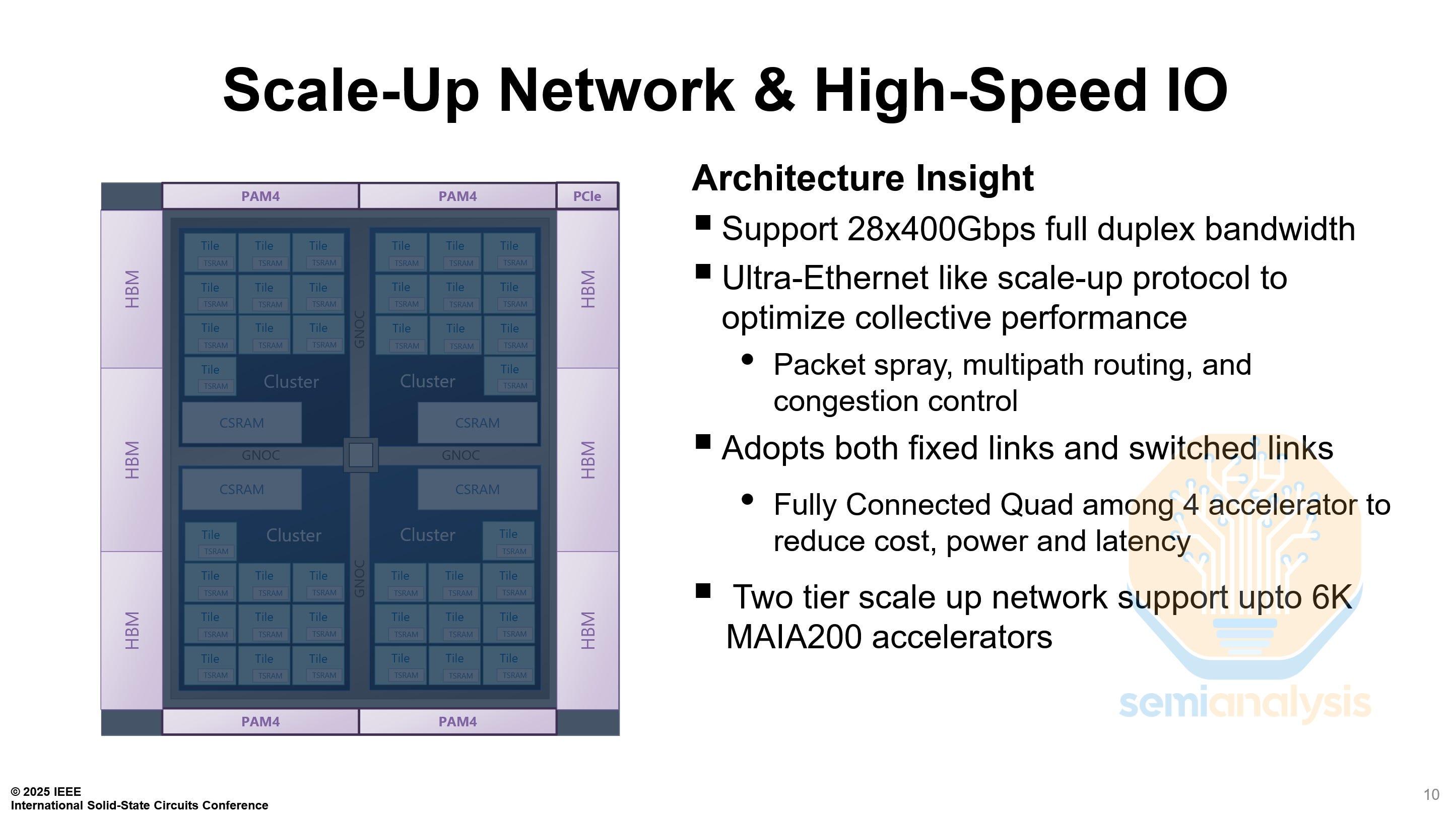
The Maia 200 has two different kinds of links, fixed links between other chips in the same node, and switched links between a chip and a switch. 21 links are configured as fixed links, 7 to each other chip, while the remaining 7 links are configured as switched links to one of four in-rack switches.
We will be publishing a deep dive into the Maia 200, its microarchitecture and network topology, for institutional subscribers.
Other Highlight
Samsung SF2 Temperature Sensor - Paper 21.5
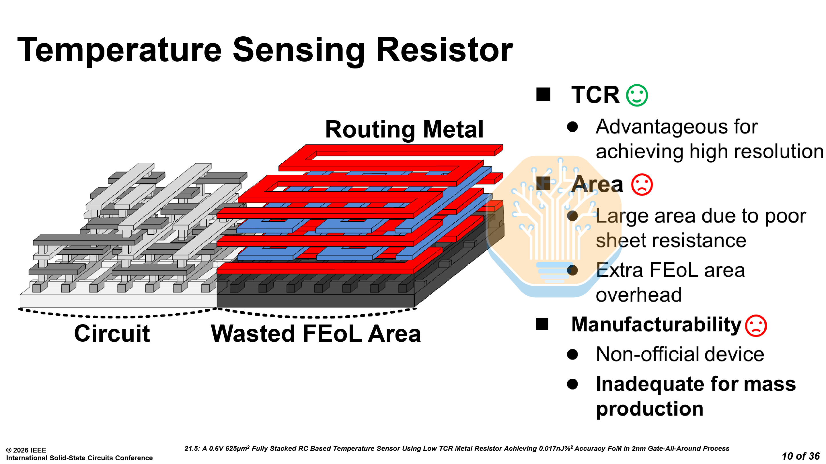
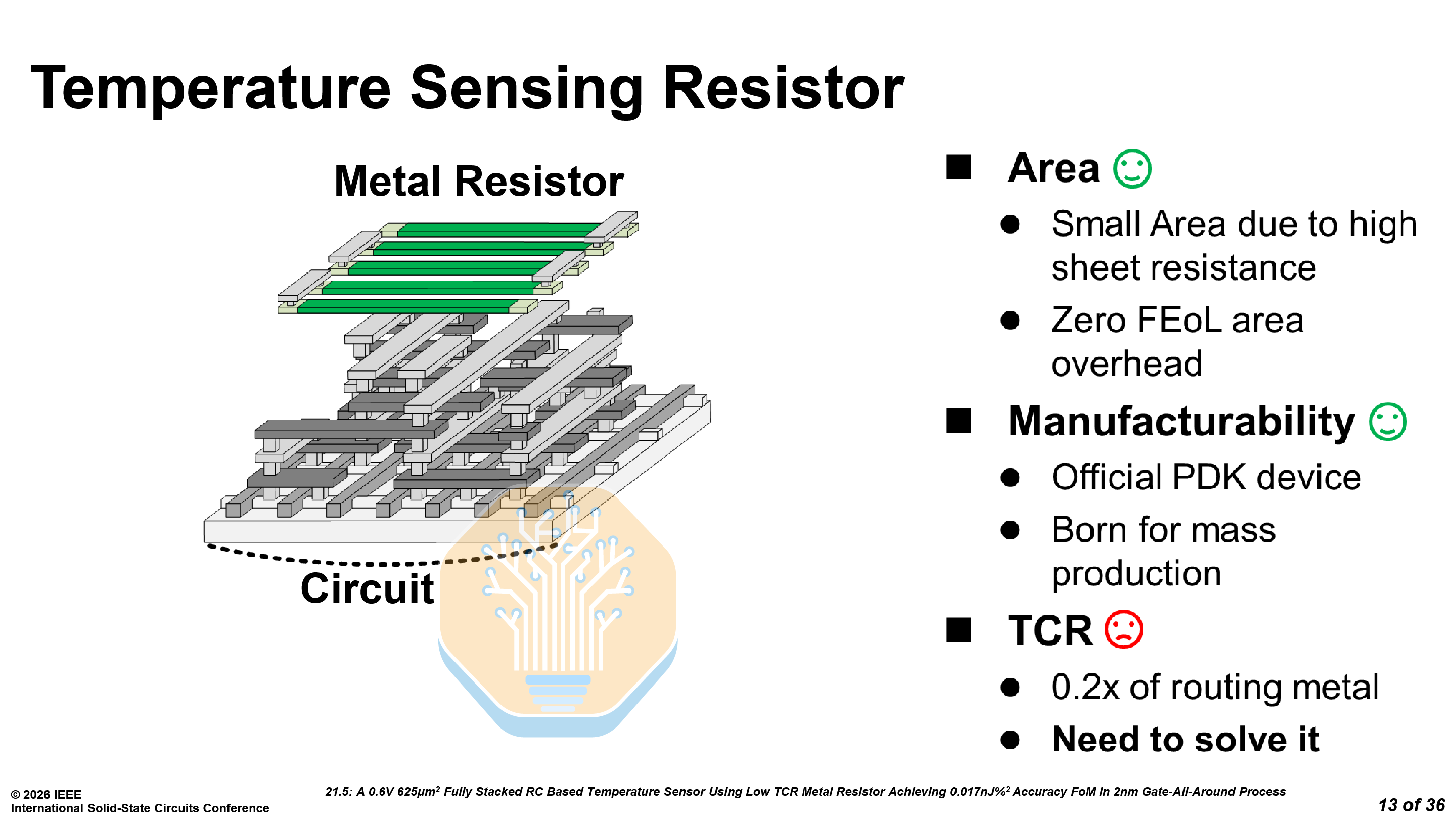
Samsung presented a compact temperature sensor on SF2, replacing the traditional bipolar junction transistor (BJT) approach with a BEOL metal resistor. This may not be as flashy as the next generation of memory or processors, but it is essential to making chips work.
The metal resistor offers 518× higher sheet resistance than an equivalent routing metal, requiring roughly 1% of the area for the same resistance. As it sits in the upper metal layers, it leaves plenty of room for any circuitry underneath and eliminates FEOL area overhead. Although it has a low resolution, the benefits more than make up for it.
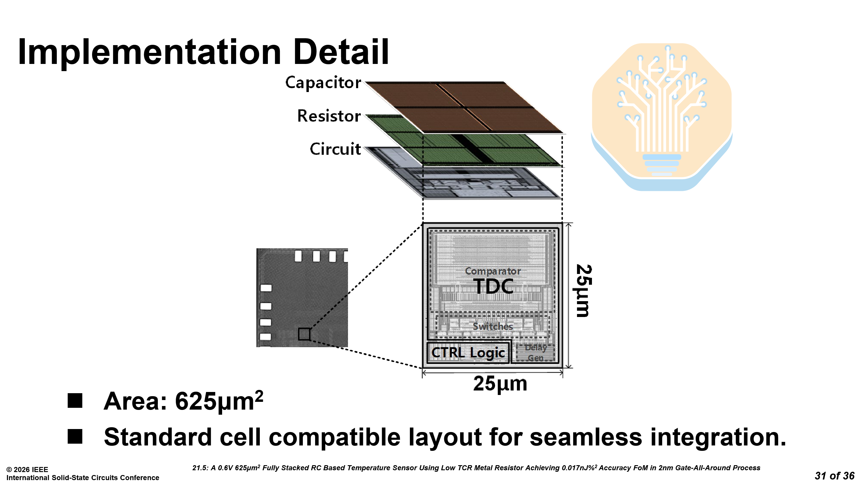
The sensor uses a fully stacked capacitor-resistor-circuit structure with a total area of just 625 μm². As a characterized PDK element, its behavior is modeled by the foundry and validated. It is more suitable for mass production, where process variation must be tightly controlled. Even on a single chip, thousands of these sensors may be used near hotspots.
As mentioned earlier, the metal resistors have a lower temperature coefficient of resistance (TCR), just 0.2× that of routing metal — which limits sensing resolution. Samsung compensates for this by increasing the base resistance. However, this slows sensing time as the RC time constant grows. To address this, Samsung uses a time-offset compression technique: a low-resistance (0.1R) fast-charge path rapidly charges the RC filter, then the circuit switches to the full resistance for the temperature-sensitive portion of the waveform.
For the time-to-digital conversion (TDC), they replaced the large linear delay generator used in prior work with a compact ring oscillator-based (RO) TDC, cutting delay generator area by 99.1%. The RO also doubles as the system clock, with phase-interleaved counting preventing non-monotonicity.
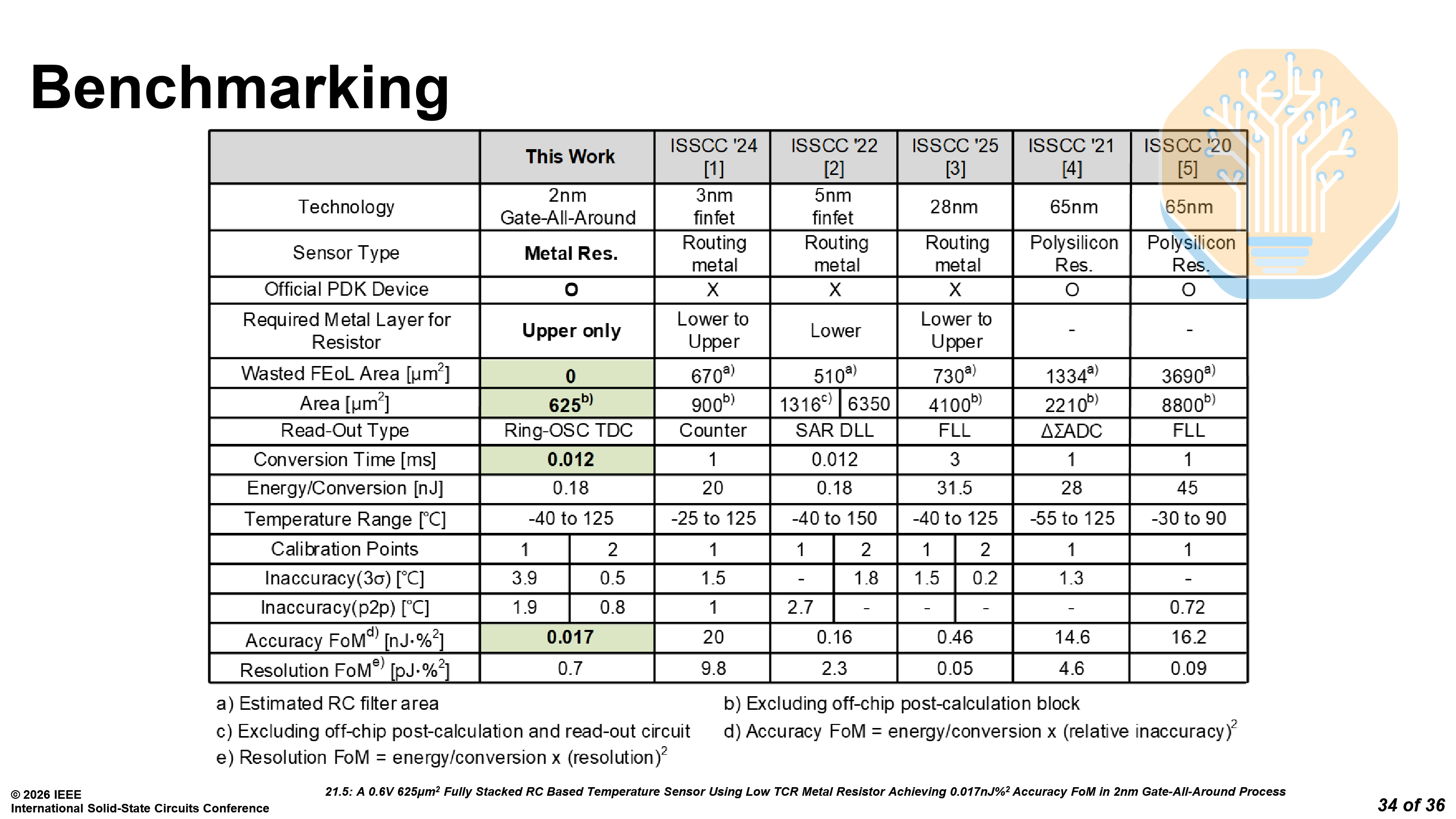
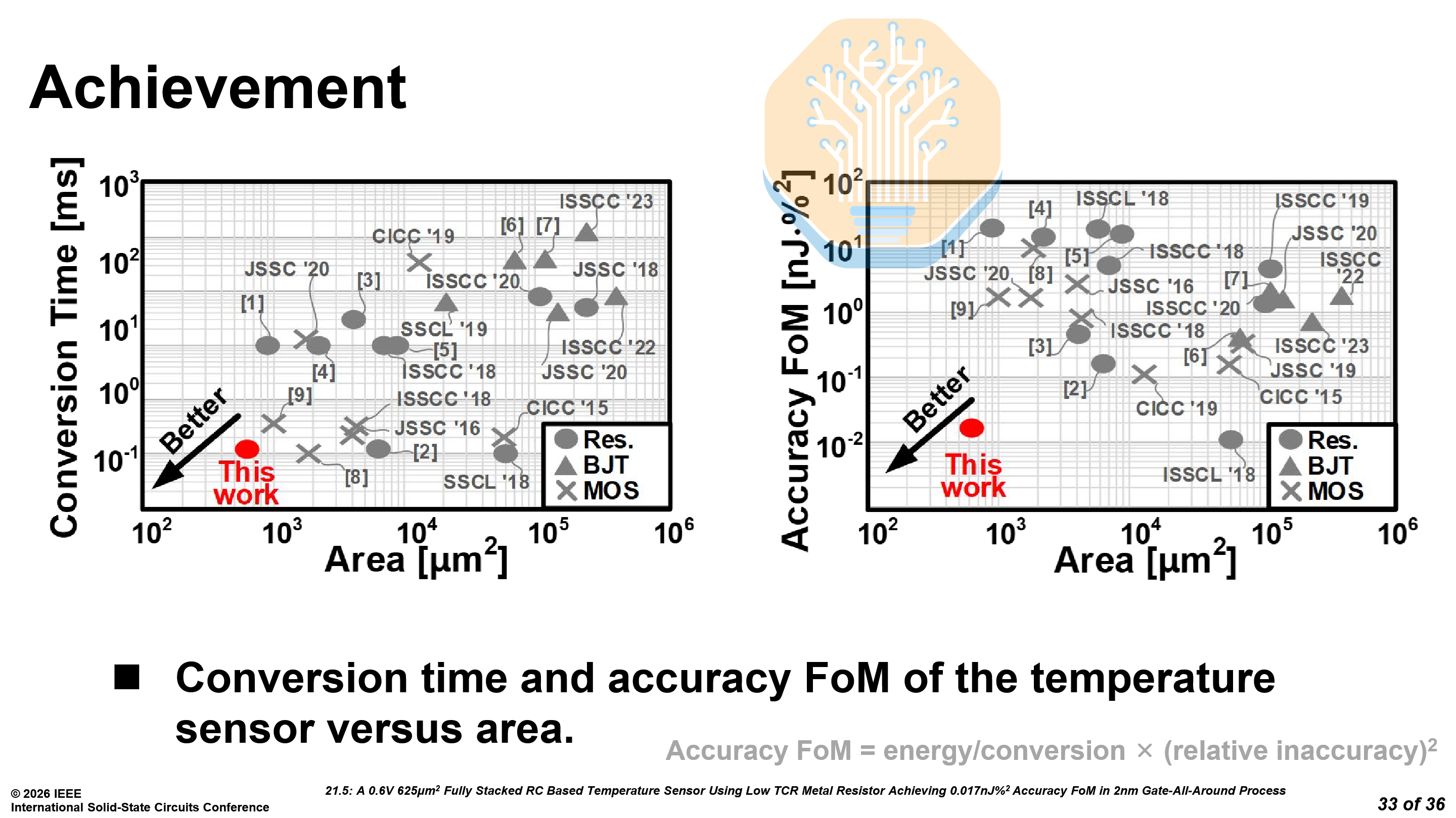
The new temperature sensor has an accuracy figure of merit (FoM) of 0.017 nJ·%², improving upon prior work on Samsung 5LPE, TSMC N3E and Intel 4 (JSSC 2025). Prior temperature sensors could only optimize for one of these: area or speed. The sensor on N3E was small, at 900 μm² but took 1 ms, while the sensor on Samsung 5LPE was fast, at 12 μs but huge, at 6356 μm².