

TPUv7: Google Takes a Swing at the King
Potential End of the CUDA Moat?, Anthropic’s 1GW+ TPU Purchase, The more (TPU) Meta/SSI/xAI/OAI/Anthro buy the more (GPU capex) you save, Next Generation TPUv8AX and TPUv8X versus Vera Rubin
The two best models in the world, Anthropic’s Claude 4.5 Opus and Google’s Gemini 3 have the majority of their training and inference infrastructure on Google’s TPUs and Amazon’s Trainium. Now Google is selling TPUs physically to multiple firms. Is this the end of Nvidia’s dominance?
The dawn of the AI era is here, and it is crucial to understand that the cost structure of AI-driven software deviates considerably from traditional software. Chip microarchitecture and system architecture play a vital role in the development and scalability of these innovative new forms of software. The hardware infrastructure on which AI software runs has a notably larger impact on Capex and Opex, and subsequently the gross margins, in contrast to earlier generations of software, where developer costs were relatively larger. Consequently, it is even more crucial to devote considerable attention to optimizing your AI infrastructure to be able to deploy AI software. Firms that have an advantage in infrastructure will also have an advantage in the ability to deploy and scale applications with AI.
Google had peddled the idea of building AI-specific infrastructure as far back as 2006, but the problem came to a boiling point in 2013. They realized they needed to double the number of datacenters they had if they wanted to deploy AI at any scale. As such, they started laying the groundwork for their TPU chips which were put into production in 2016. It’s interesting to compare this to Amazon, who in the same year, realized they needed to build custom silicon too. In 2013, they started the Nitro Program, which was focused on developing silicon to optimize general-purpose CPU computing and storage. Two very different companies optimized their efforts for infrastructure for different eras of computing and software paradigms.
We’ve long believed that the TPU is among the world’s best systems for AI training and inference, neck and neck with king of the jungle Nvidia. 2.5 years ago we wrote about TPU supremacy, and this thesis has proven to be very correct.

TPU’s results speak for themselves: Gemini 3 is one of the best models in the world and was trained entirely on TPUs. In this report, we will talk about the huge changes in Google’s strategy to properly commercialize the TPU for external customers, becoming the newest and most threatening merchant silicon challenger to Nvidia.
We plan to:
(Re-)Educate our clients and new readers about the rapidly growing commercial success of external TPU customers, starting with Anthropic and extending to Meta, SSI, xAI and even potentially OpenAI...
Show that: The more (TPU) you buy, the more (NVIDIA GPU capex) you save! OpenAI hasn’t even deployed TPU yet and already increased perf per TCO by getting ~30% off their compute fleet due to competitive threats
Explain the circular economy deals for AI Infrastructure.
Revisit our original TPU deep dive with a refresher on the TPU hardware stack from silicon down to the software layer.
Cover the positive developments on the open software ecosystem front as well as the critical missing ingredient for Google to make the TPU ecosystem a viable challenger to the CUDA moat: open source their XLA:TPU compiler, runtime, and multi-pod “MegaScaler” code.
In the paywall, we will discuss the implications for Nvidia’s moat and compare Vera Rubin to the next gen TPUv8AX/8X (aka Sunfish/Zebrafish)
Also cover the long term threat to Nvidia.
First, let’s talk about the impact this news has had on the ecosystem. TPU performance has clearly caught the attention of its rivals. Sam Altman has acknowledged “rough vibes” ahead for OpenAI as Gemini has stolen the thunder from OpenAI. Nvidia even put out a reassuring PR telling everyone to keep calm and carry on — we are well ahead of the competition.
We understand why. These past few months have been win after win for the Google Deepmind, GCP, and TPU complex. The huge upwards revisions to TPU production volumes, Anthropic’s >1GW TPU buildout, SOTA models Gemini 3 and Opus 4.5 trained on TPU, and now an expanding list of clients being targeted (Meta, SSI, xAI, OAI) lining up for TPUs. This has driven a huge re-rating of the Google and TPU supply chain at the expense of the Nvidia GPU-focused supply chain. While the “sudden” emergence of Google and the TPU supply chain has caught many by surprise, SemiAnalysis institutional product subscribers have been anticipating this for the last year.
Another reason Nvidia has been on the defensive is a growing chorus of skeptics who argue the company is propping up a “circular economy” by funding cash-burning AI startups, essentially moving money from one pocket to another with extra steps. We think this view is misplaced, but it has clearly struck a nerve inside Nvidia. The finance team issued a detailed response, reproduced below.
We think a more realistic explanation is that Nvidia aims to protect its dominant position at the foundation labs by offering equity investment rather than cutting prices, which would lower Gross margins and cause widespread investor panic. Below, we outline the OpenAI and Anthropic arrangements to show how frontier labs can lower GPU TCO by buying, or threatening to buy TPUs.
OpenAI hasn’t even deployed TPUs yet and they’ve already saved ~30% on their entire lab wide NVIDIA fleet. This demonstrates how the perf per TCO advantage of TPUs is so strong that you already get the gains from adopting TPUs even before turning one on.
Our Accelerator Industry Model, Datacenter Industry Model and Core Research subscribers saw the industry implications well before this was announced and became market consensus. In early August, we shared with our Accelerator Model clients that we saw massive upward revisions for Broadcom / Google TPU orders in the supply chain for 2026. We also revealed that the reason for these order increases was the fact that Google would begin selling systems externally to multiple customers. In early September, we revealed that one of the big external customers will be Anthropic, with demand of at least 1 million TPUs. This was officially confirmed by Anthropic and Google in October. We also called out Meta as a big TPU customer on the 7th of November, weeks before others. In addition we have discussed other customers as well.
As a result, our institutional clients have had plenty of heads up on one of the largest performance dispersions in the AI Trade to date. SemiAnalysis was the first to break all these insights because no other research firm can connect the dots from the fabs to supply chain through the datacenters to the labs. To get access to these insights as and stay ahead of the curve: sales@semianalysis.com
Onto the deal.
Google’s Big TPU Externalization Push and The Anthropic Deal
The TPU stack has long rivaled Nvidia’s AI hardware, yet it has mostly supported Google’s internal workloads. In typical Google fashion, it never fully commercialized the TPU even after making it available to GCP customers in 2018. That is starting to change. Over the past few months, Google has mobilized efforts across the whole stack to bring TPUs to external customers through GCP or by selling complete TPU systems as a merchant vendor. The search giant is leveraging its strong in-house silicon design capabilities to become a truly differentiated cloud provider. Furthermore, it aligns with marquis customer Anthropic’s continued push to diversify away from its dependence on NVDA.
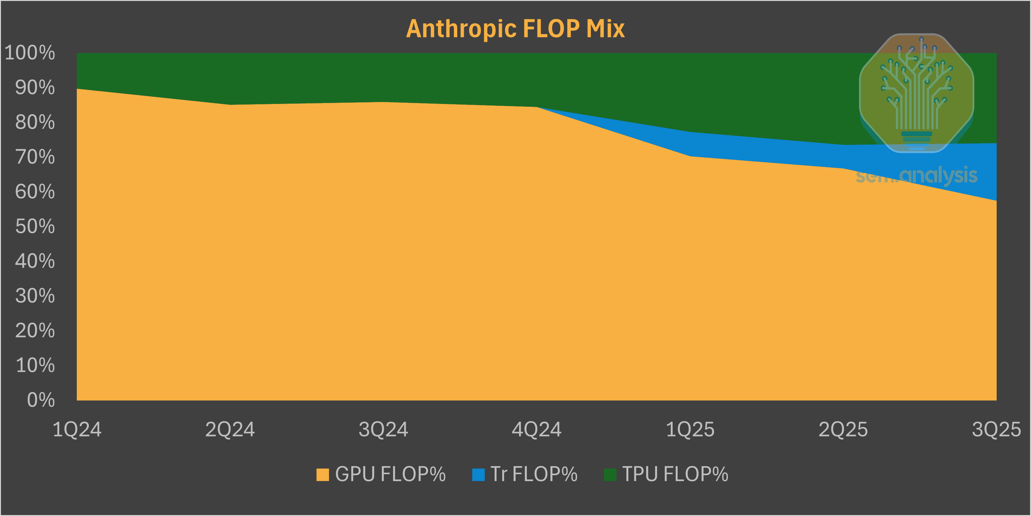
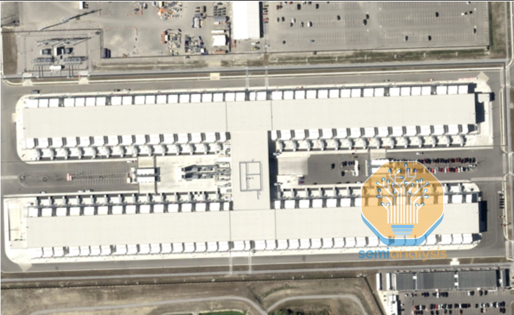
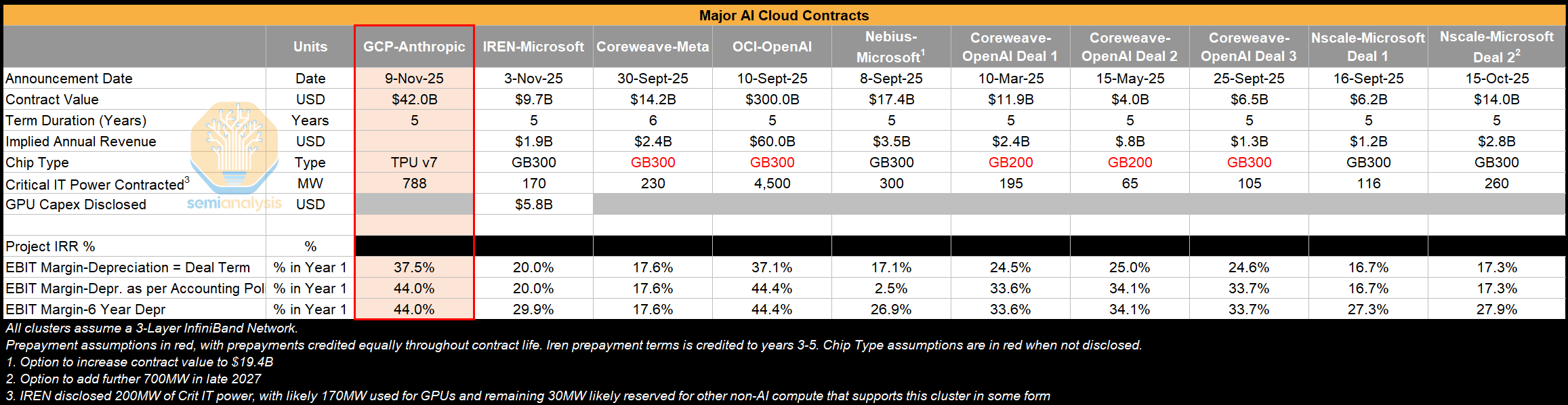
The Anthropic deal marks a major milestone in this push. We understand that GCP CEO Thomas Kurian played a central role in the negotiations. Google committed early by investing aggressively in Anthropic’s funding rounds, even agreeing to no voting rights and a 15% cap on their ownership to expand the use of TPUs beyond internal Google. This strategy was eased by the presence of former DeepMind TPU talent within the foundation lab, resulting in Anthropic training Sonnet and Opus 4.5 on multiple types of hardware including TPUs. Google has already built a substantial facility for Anthropic, as shown below as part of our building-by-building tracker of AI labs.
Beyond renting capacity in Google datacenters through GCP, Anthropic will deploy TPUs in its own facilities, positioning Google to compete directly with Nvidia as a true merchant hardware vendor.
In terms of the split of the 1M TPUs:
The first phase of the deal covers 400k TPUv7 Ironwoods, worth ~$10 billion in finished racks that Broadcom will sell directly to Anthropic. Anthropic is the fourth customer referenced in Broadcom’s most recent earnings call. Fluidstack, a gold-rated ClusterMax Neocloud provider, will handle on-site setup, cabling, burn-in, acceptance testing, and remote hands work as Anthropic offloads managing physical servers. DC infrastructure will be supplied by TeraWulf (WULF) and Cipher Mining (CIFR).
The remaining 600k TPUv7 units will be rented through GCP in a deal we estimate at $42 billion of RPO, accounting for most of the $49 billion increase in GCP’s backlog reported in the third quarter.
We believe additional deals with Meta, OAI, SSI, and xAI could provide additional RPO + direct hardware sales for GCP in coming quarters.
Despite heavy internal and external demand, Google has not been able to deploy TPUs at the pace it wants. Even though it has more control over its hardware supply than other hyperscalers that still need curry favor with Jensen, Google’s main bottleneck is power.
While other hyperscalers have expanded their own sites and secured significant colocation capacity, Google has moved more slowly. We believe the core issue is contractual and administrative. Each new datacenter vendor requires a Master Services Agreement, and these are multibillion-dollar, multiyear commitments that naturally involve some bureaucracy. Yet Google’s process is especially slow, often taking up to three years from initial discussions to a signed MSA.
Google’s workaround carries major implications for Neocloud providers and cryptominers looking to pivot to AI DC infrastructure. Instead of leasing directly, Google offers a credit backstop, an off-balance-sheet “IOU” to step in if Fluidstack cannot pay its datacenter rent.
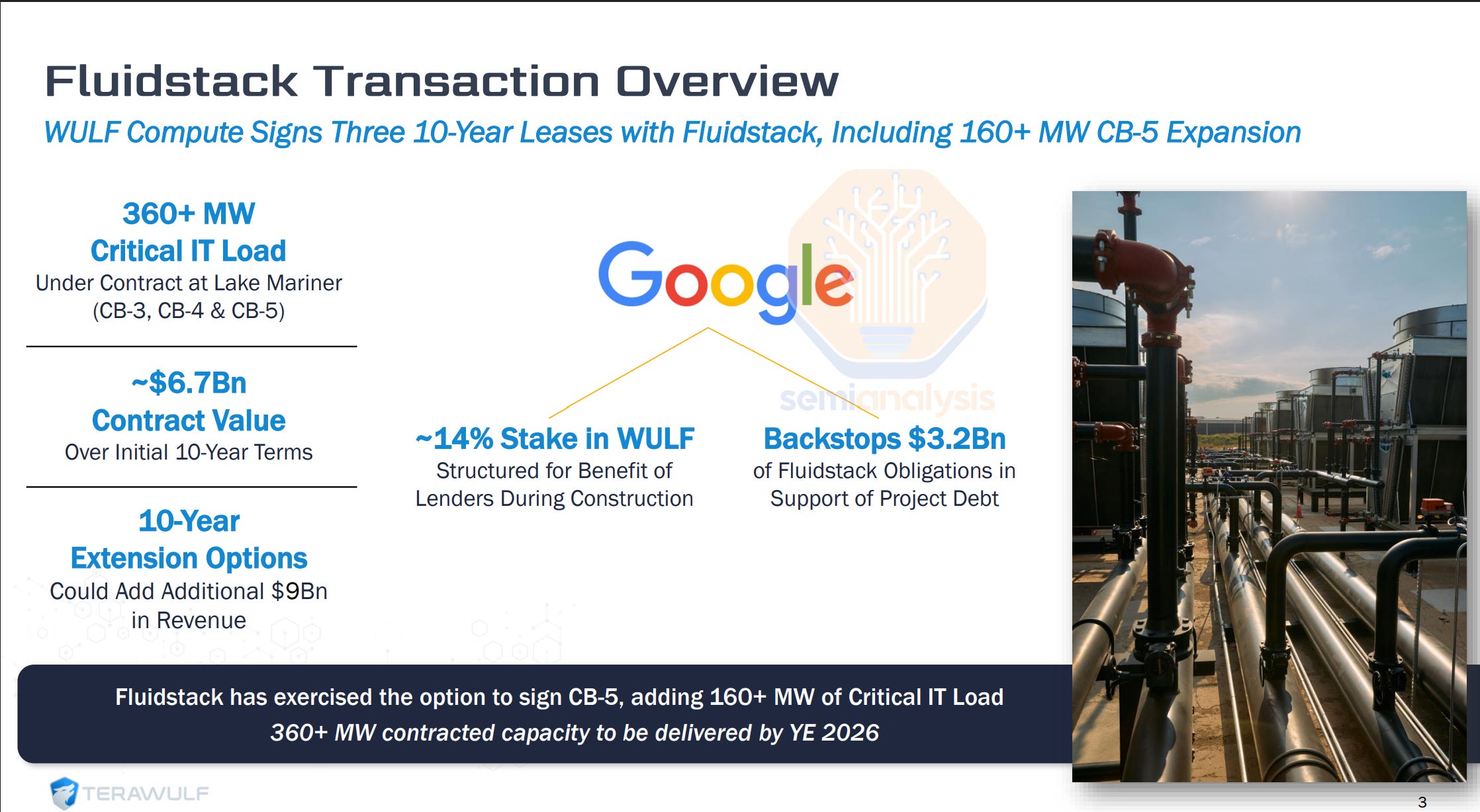
Neoclouds like Fluidstack are nimble and flexible, making it easier for them to deal with new datacenter vendors like reformed cryptominers. This mechanic has been key to our bullish views on the cryptomining industry – notably we were calling out numerous including IREN and Applied Digital at the beginning of the year when stock prices were materially lower.
The opportunity for miners rests on a simple dynamic: the datacenter industry faces acute power constraints power, and cryptominers already control capacity through their PPAs and existing electrical infrastructure. We expect many more agreements to follow in the coming weeks and quarters.
How Google reshaped the Neocloud market
Prior to the Google/Fluidstack/TeraWulf deal, we had not seen any deal with a mere off-balance-sheet “IOU” in the Neocloud market. After the deal, we believe it has become the new de-facto standard financing template. This solves a key headache for Neoclouds looking to secure datacenter capacity and grow their business:
A GPU cluster has a useful and economic life of 4-5years
A large datacenter lease is typically 15+ years, with a typical payback period of ~8 years.
This duration mismatch has made it very complicated for both Neoclouds and Datacenter vendors to secure financing for projects. But with the rise of the “hyperscaler backstop”, we believe the financing issues are solved. We expect a new wave of growth for the NeoCloud industry. Check out our Accelerator and Datacenter models to understand the key beneficiaries. These are the how’s and why’s behind the Anthropic deal, now let’s get into the hardware.
Furthermore, Neoclouds who count Jensen as an investor such as CoreWeave, Nebius, Crusoe, Together, Lambda, Firmus, and Nscale all have a notable incentive to not adopt any competing technology in their datacenter: TPUs, AMD GPUs, or even Arista switches are off limits! This leaves a gaping hole in the market for TPU hosting that is currently filled by a combination of crypto miners + Fluidstack. In the coming months, we expect to see more Neoclouds make the tough decision between pursuing a growing TPU hosting opportunity and securing allocations of the latest and greatest Nvidia Rubin systems.
TPUv7 Ironwood – Why do Anthropic and other customers want TPU?
The answer is simple. It is a strong chip inside an excellent system, and that combination offers compelling performance and TCO for Anthropic. 2.5 years ago, we wrote about Google’s compute infrastructure advantage. Even with silicon that lagged Nvidia’s on paper, Google’s system-level engineering allowed the TPU stack to match Nvidia in both performance and cost efficiency.
We argued then that “systems matter more than microarchitecture,” and the past two years have reinforced that view. Anthropic’s massive TPU orders are a direct validation of the platform’s technical strength. The GPU ecosystem has shifted forward as well. Nvidia’s GB200 represents a major leap forward, pushing Nvidia toward becoming a true systems company that designs full servers rather than only the chip package inside.
While we are on the topic of the GB200’s huge innovation in rack-scale interconnect, one underappreciated point is that Google has been scaling up TPUs within and across racks since TPU v2 back in 2017! Further down in the report, we feature a deep dive on Google’s ICI scale-up networking, the only real rival to Nvidia’s NVLink.
Google’s recent Gemini 3 model is now viewed as the state of the art frontier LLM. Like all earlier versions of Gemini, it was trained entirely on TPUs. That result offers concrete proof of both TPU capability and Google’s broader infrastructure advantage.
Today’s attention often centers on hardware for inference and post-training, yet pre-training a frontier model remains the hardest and most resource-intensive challenge in AI hardware. The TPU platform has passed that test decisively. This stands in sharp contrast to rivals: OpenAI’s leading researchers have not completed a successful full-scale pre-training run that was broadly deployed for a new frontier model since GPT-4o in May 2024, highlighting the significant technical hurdle that Google’s TPU fleet has managed to overcome.
One of the key highlights of the new model include noticeable gains in tool calling and agentic capability, especially on longer-horizon tasks for economically valuable tasks. Vending Bench is an evaluation that aims to measure how well models would run a business over a long period of time by placing them as the owner of a simulated vending machine business and Gemini 3 destroyed the competition.
This launch brought not just improved capabilities but new products. Antigravity, a product born from the acqui-hire of former Windsurf CEO Varun Mohan and team, is Google’s answer to OpenAI’s Codex, officially entering Gemini into the vibe coding token guzzling wars.
For Google to quietly muscle in and establish a performance lead in one of the most challenging hardware problems is a truly impressive feat for a company whose core business isn’t, or should we say, wasn’t in hardware business.
Microarchitecture is still a big deal: Ironwood nears Blackwell
The corollary to “Systems matter more than Microarchitecture”, is that while Google has been pushing the boundary on system and networking design, TPU silicon itself wasn’t too ground-breaking. Since then, TPU silicon has made massive strides with the latest generations.
From the outset, Google’s design philosophy has been more conservative on silicon relative to Nvidia. Historically, TPUs have shipped with significantly fewer peak theoretical FLOPs, and lower memory specs than corresponding Nvidia GPUs.
There are 3 reasons for this. First, Google places a high internal emphasis on ‘RAS’ (Reliability, Availability, and Serviceability) for their infrastructure. Google prefers to sacrifice absolute performance in exchange for greater hardware uptime. Running things to the limit means higher instances of hardware mortality which has a real TCO impact in terms of system downtime and hot spares. After all, the hardware you cannot use has infinite TCO relative to performance.
The second reason is that up until 2023, Google’s primary AI workload was recommendation system models to power their core Search and Ad properties. RecSys workloads carry much lower arithmetic intensity compared to LLM workloads which means fewer FLOPs are required relative to every bit of data that is transferred.
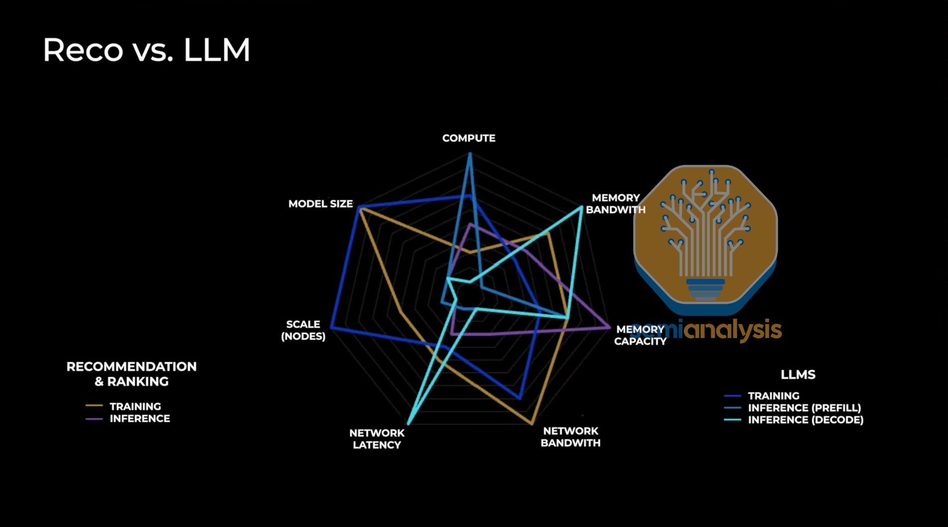
The third comes down to the utility of “peak theoretical FLOPs” numbers that are marketed and how they can be manipulated. Merchant GPU providers like Nvidia and AMD want to market the best performance specifications possible for their chips. This incentivizes them to stretch marketed FLOPs to the highest number possible. In practice, these numbers are unable to be sustained. On the other hand, the TPU has primarily been internal facing, with much less pressure to inflate these specifications externally. This has important implications that we’ll discuss further. The generous way to look at it would be Nvidia is better at DVFS therefore happy to report peak specs only.
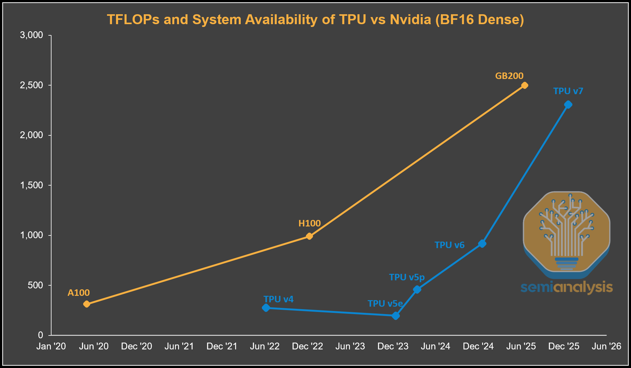
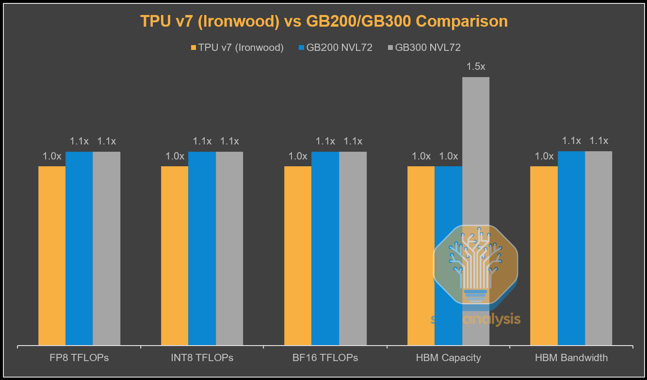
After we ushered in the LLM era, there has been a clear shift in Google’s TPU design philosophy. We can see that with the 2 most recent TPU generations that were designed-post LLM: TPUv6 Trillium (Ghostlite) and TPUv7 Ironwood (Ghostfish) reflect that change. We can see in the chart below that for TPUv4 and v5, compute throughput was much lower than the Nvidia flagship at the time. TPUv6 came very close to the H100/H200 on FLOPs, but it came 2 years later than the H100. With TPU v7, the gap narrows further with servers available only a few quarters later, while delivering almost the same level of peak theoretical FLOPs.
What drove these performance gains? Partially it’s that Google started announcing TPUs as they ramp into production rather then after the next generation was being deployed. Furthermore, TPU v6 Trillium is manufactured on the same N5 node as TPU v5p with similar silicon area but was able to deliver a whopping 2x increase in peak theoretical FLOPs with significantly less power! For Trillium, Google quadrupled the size of each systolic array to 256 x 256 tiles from 128 x 128, and this increase in array size is what has delivered the increase in compute.
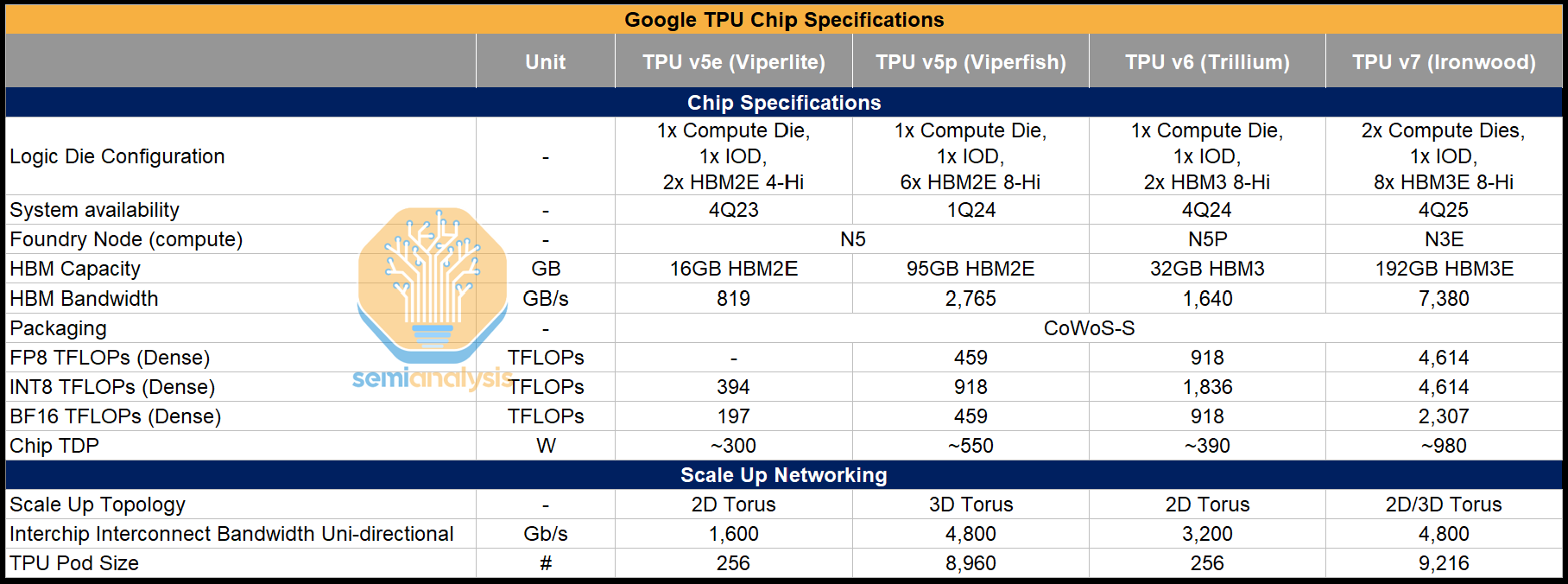
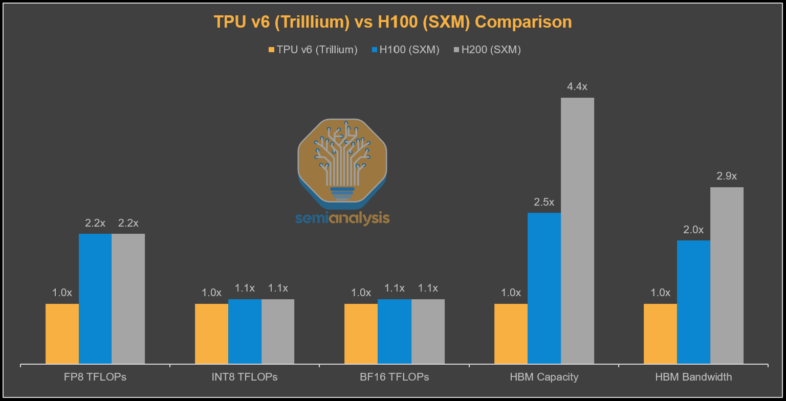
Trillium was also the last of the “E” (lite) SKUs which meant it was equipped with only 2 sites of HBM3. While Trillium closed the gap to Hopper on compute, it fell far short of the H100/H200 on memory capacity and bandwidth, with only 2 stacks of HBM3 vs 5 and 6 stacks of HBM3 and HBM3E respectively. This made it painful to use for novices, but the performance TCO achieved for Trillium is unbeatable if you get shard your model properly and utilize all those cheap FLOPS.
TPU v7 Ironwood is the next iteration where Google nearly completely closes the gap to the corresponding Nvidia flagship GPU on FLOPs, memory, and bandwidth albeit with general availability 1 year later than Blackwell. Compared to the GB200, FLOPs and memory bandwidth only have a slight shortfall, with capacity being the same with 8-Hi HBM3E, which is of course a significant shortfall to GB300 which has 288GB of 12-Hi HBM3E.
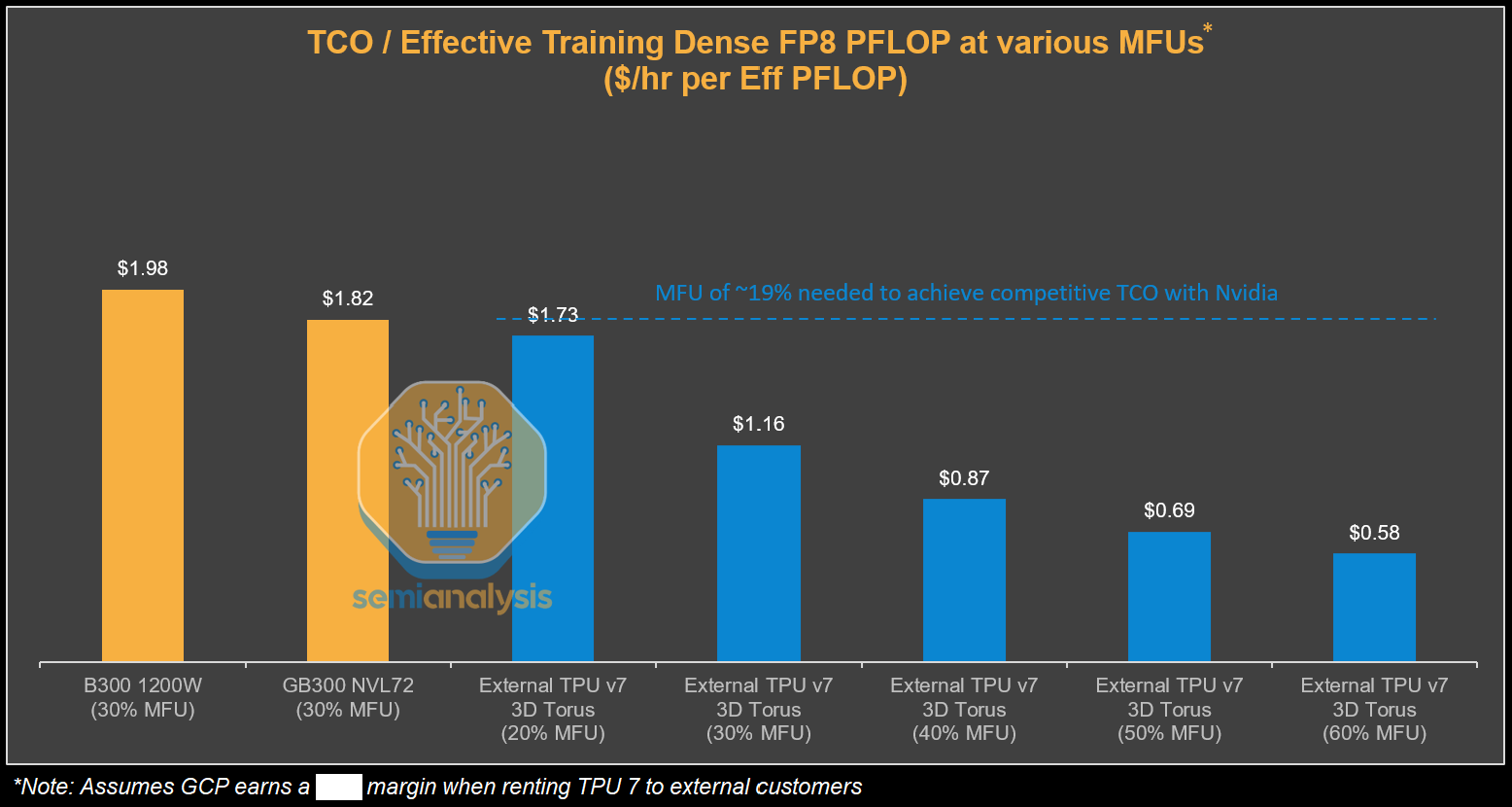
Theoretical absolute performance is one thing but what matters is real world performance per Total Cost of Ownership (TCO).
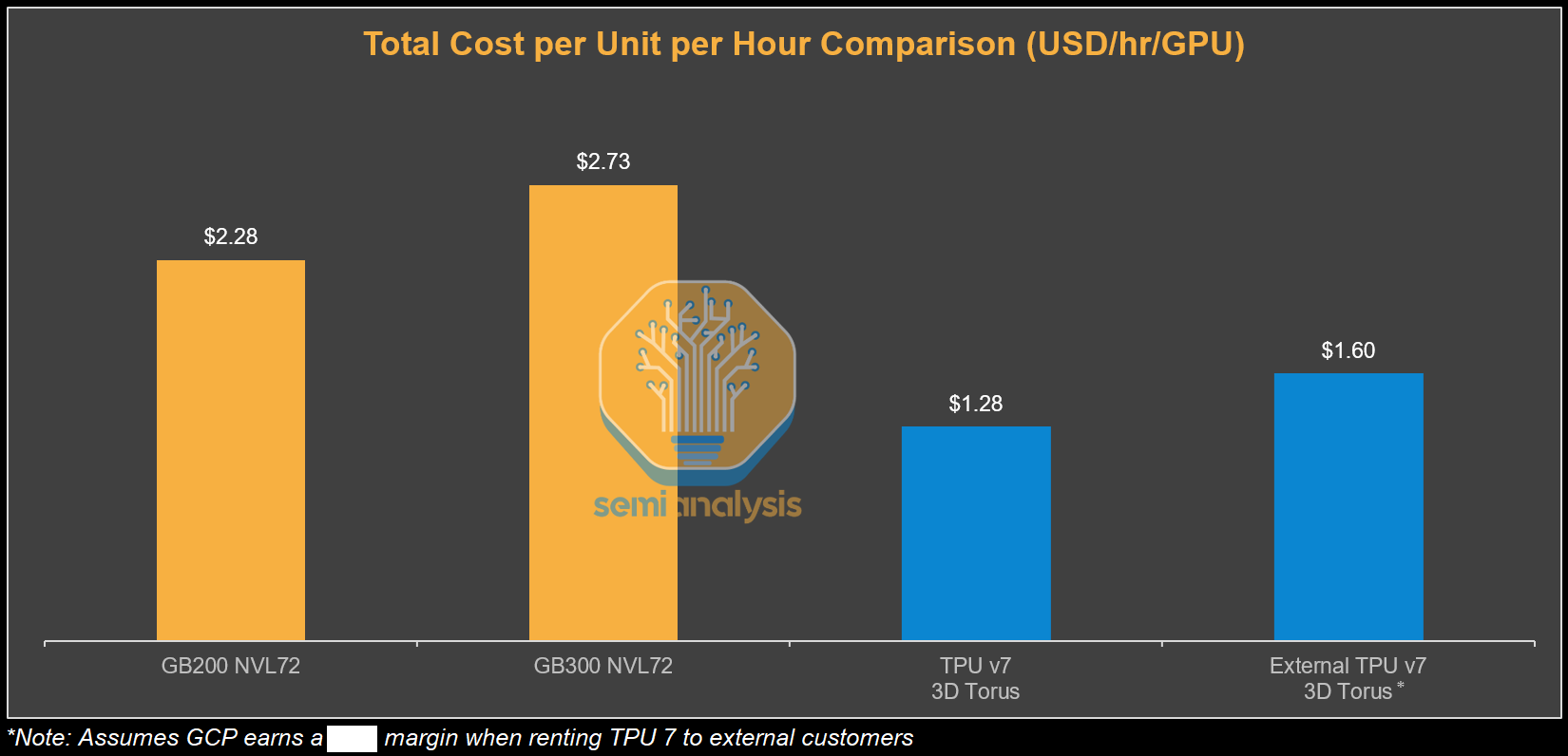
While Google procures TPUs through Broadcom and pays a hefty margin, it is significantly less than the margin Nvidia earns on not only the GPUs they sell but entire the whole system including CPUs, Switches, NICs, system memory, cabling and connectors. From Google’s perspective this results in the all-in TCO per Ironwood chip for the full 3D Torus configuration being ~44% lower than the TCO of a GB200 server.
This more than makes up for the ~10% shortfall on peak FLOPs and peak memory bandwidth. This is from the perspective of Google and the price they procure TPU servers at.
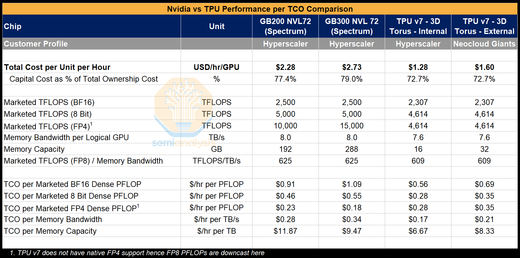
What about Google’s external customers when Google adds their margin on top? We assume that in the case where Google earns a margin on leasing TPU 7 to external customers that the TCO per hour can still be up to ~30% lower than the cost of the GB200 and ~41% lower than the cost of the GB300. This is what we believe is reflective of Anthropic’s pricing via GCP.
Why Anthropic Is Betting on TPUs
Comparing theoretical FLOPs tells only part of the story. What matters is effective FLOPs, since peak numbers are almost never reached in real-world workloads.
In practice, Nvidia GPUs typically achieve only about a small portion of their theoretical peak once communication overhead, memory stalls, power limits, and other system effects are factored in. A good rule of thumb for training is 30%, but utilization also varies heavily by workload. A large share of the gap comes down to software and compiler efficiency. Nvidia’s advantage here stems from the CUDA moat and the wide set of open source libraries that come out of the box, helping workloads run efficiently with high realized FLOPs and memory bandwidth.
The TPU software stack is not as easy to use, though this is beginning to change. Inside Google, TPUs benefit from excellent internal tooling that is not exposed to external customers, which makes out of the box performance weaker. However, this only applies to small and/or lazy users, and Anthropic is neither of those.
Anthropic has strong engineering resources and ex-Google compiler experts who know both the TPU stack and understand their own model architecture well. They can invest in custom kernels to drive high TPU efficiency. As a result, they can reach substantially higher MFU and much better $/PFLOP performance.
We believe that despite lower marketed peak FLOPs, TPUs can reach higher realized Model FLOP Utilization (MFU) than Blackwell, which translates into higher effective FLOPs for Ironwood. A major reason is that marketed GPU FLOPs from Nvidia and AMD are significantly inflated. Even in tests designed to maximize throughput through GEMMs shaped far from real workloads, Hopper only reached about ~80% of peak, Blackwell landed in the 70s, and AMD’s MI300 series in the 50s-60s.
The limiting factor is power delivery. These chips cannot sustain the clock speeds used in the peak math. Nvidia and AMD implement Dynamic Voltage and Frequency Scaling which means that the chip’s clock frequency is dynamically adjusted based on power consumption and thermals rather than a stable clock frequency that can actually be sustained. Nvidia and AMD then select the highest clock frequency that could possibly be delivered, even if very intermittently, to be used in the calculation of peak theoretical FLOPs (operations per cycle per ALU x number of ALUs x cycles per second i.e. clock frequency).
There are other tricks that are employed, like running GEMMs on tensors filled with zeroes, as 0x0=0, the transistors don’t need to switch state from 0 to 1, therefore reducing the power draw of each operation. Of course, in the real world, zero-filled tensors are not multiplied together.

When we put together much lower TCO and higher effective FLOPs utilization, from the perspective of Google the $ per effective FLOP becomes much cheaper, with ~15% MFU being the breakeven with GB300 at 30% MFU. This means if Google (or Anthropic) manages to hit half the FLOPs utilization of GB300, they still come out even. Of course, with Google’s elite compiler engineer team and deep understanding of their own models, the MFU they can realize on TPUs could be 40% potentially. That would be a whopping ~62% reduction in cost per effective training FLOP!
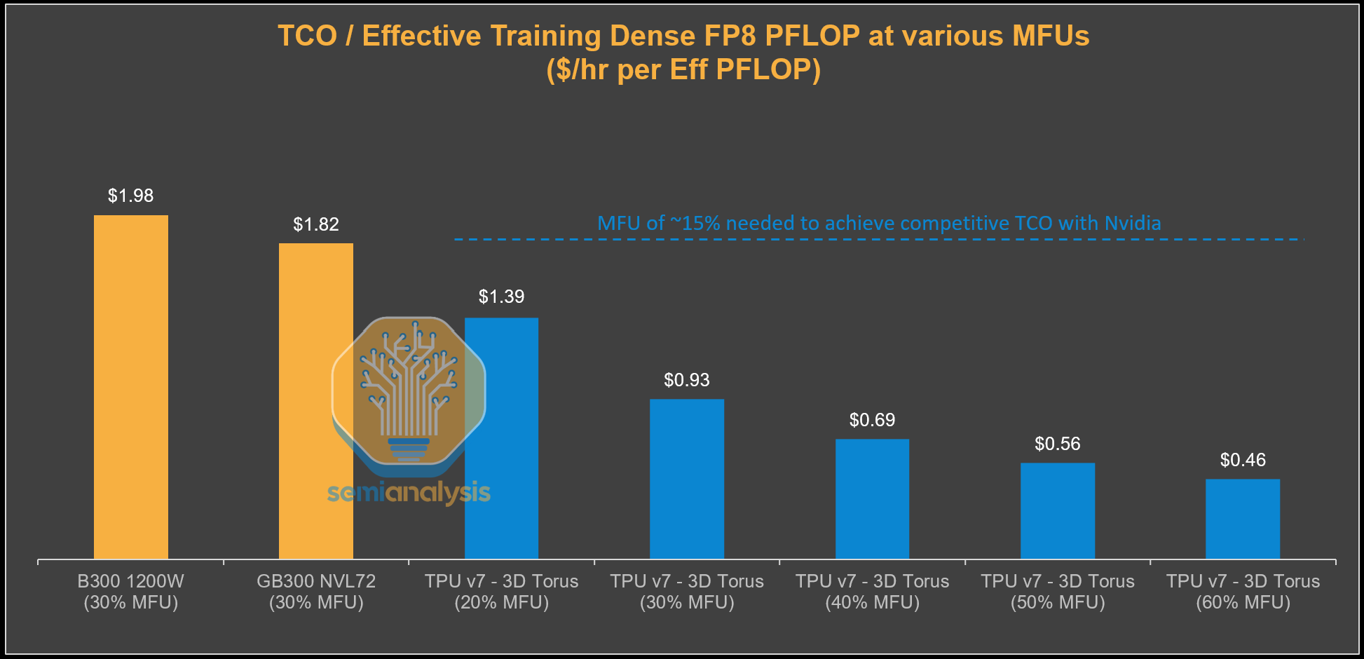
However, when looking at the 600K rented TPUs, when we incorporate the higher TCO that Anthropic pays (ie inclusive of Google’s margin stacking) into this analysis, we estimate the cost to Anthropic to be $1.60 per TPU-hour from GCP, narrowing the TCO advantage. We believe that Anthropic can realize 40% MFU on TPUs due to both their focus on performance optimization as well as the TPU’s marketed FLOPs inherently being more realistic. This provides Anthropic with a staggering ~52% lower TCO per effective PFLOP compared to GB300 NVL72. The equilibrium where TCO per effective FLOP compared to the GB300 baseline is the same is at a much lower 19% extracted MFU for Anthropic. This means that Anthropic can suffer a sizeable performance shortfall relative to the baseline GB300 and the perf/TCO for training FLOPs still ends up being the same as the baseline Nvidia system.
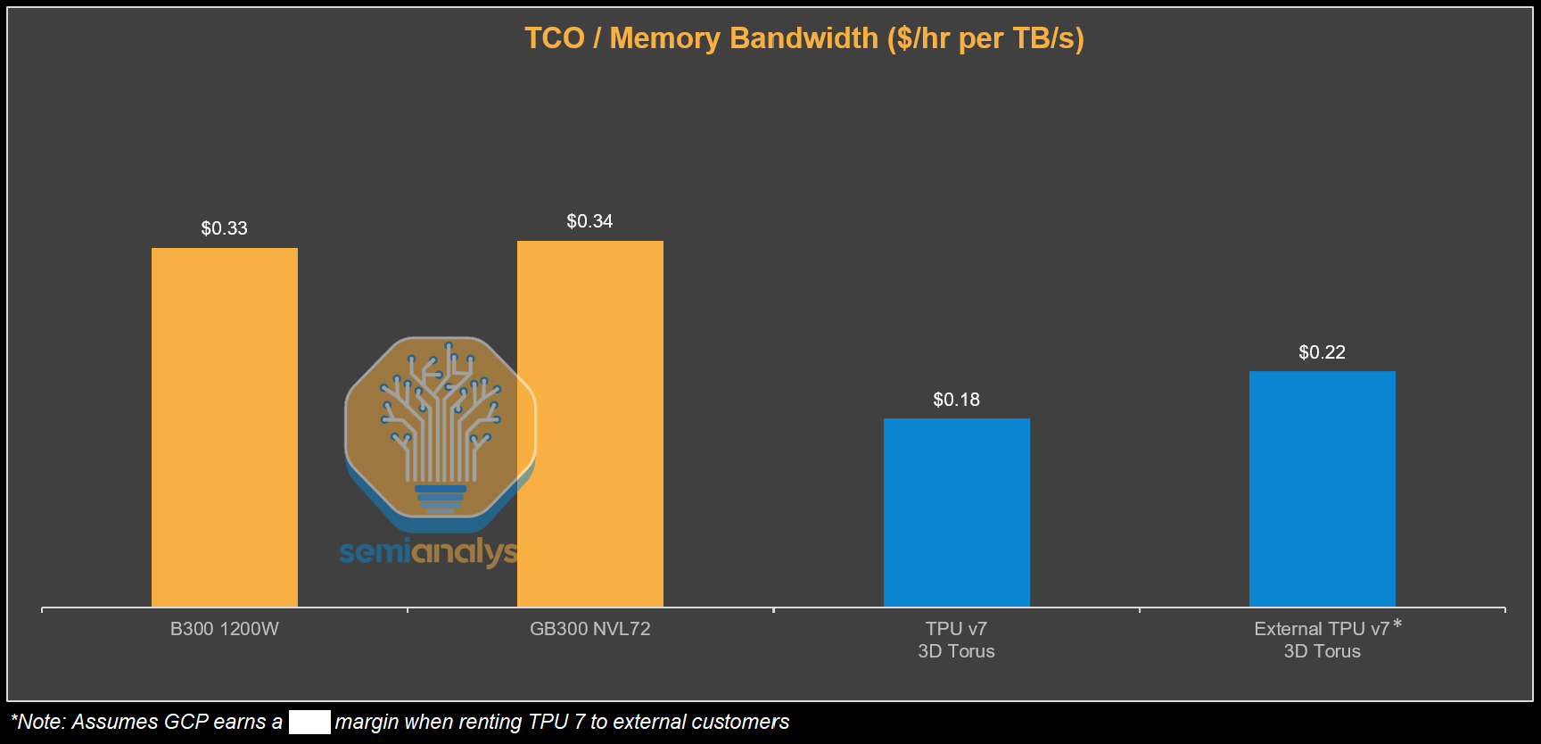
FLOPs are not the end all and be all for performance, memory bandwidth is super important for inference, especially on the bandwidth intensive decode step. It should be no surprise that $ per memory bandwidth for the TPU also ends up being much cheaper than GB300. There is significant evidence that at small message sizes such as 16MB to 64MB (loading an expert of a single layer), TPU’s even achieve higher memory bandwidth utilization then GPUs.
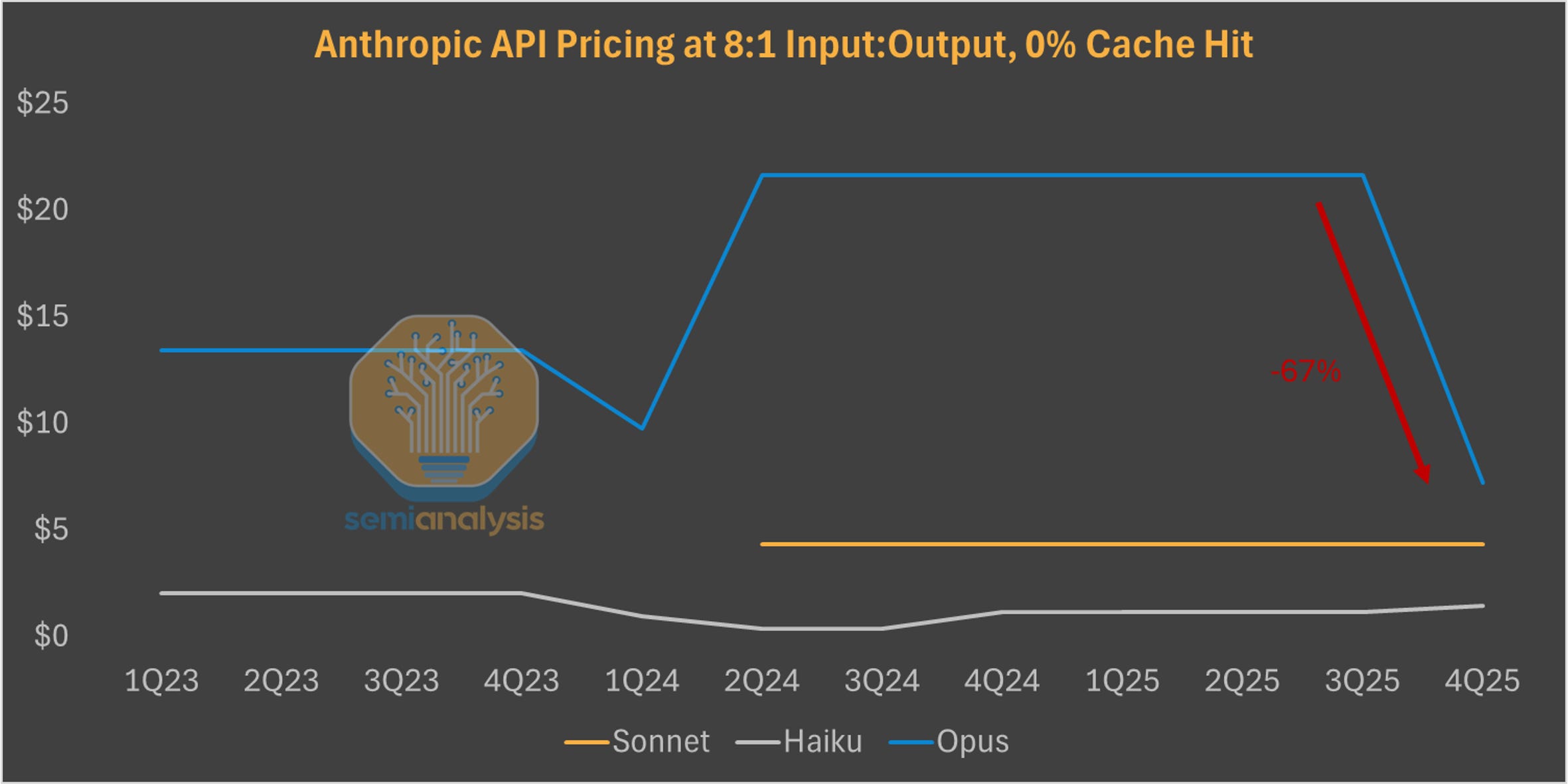
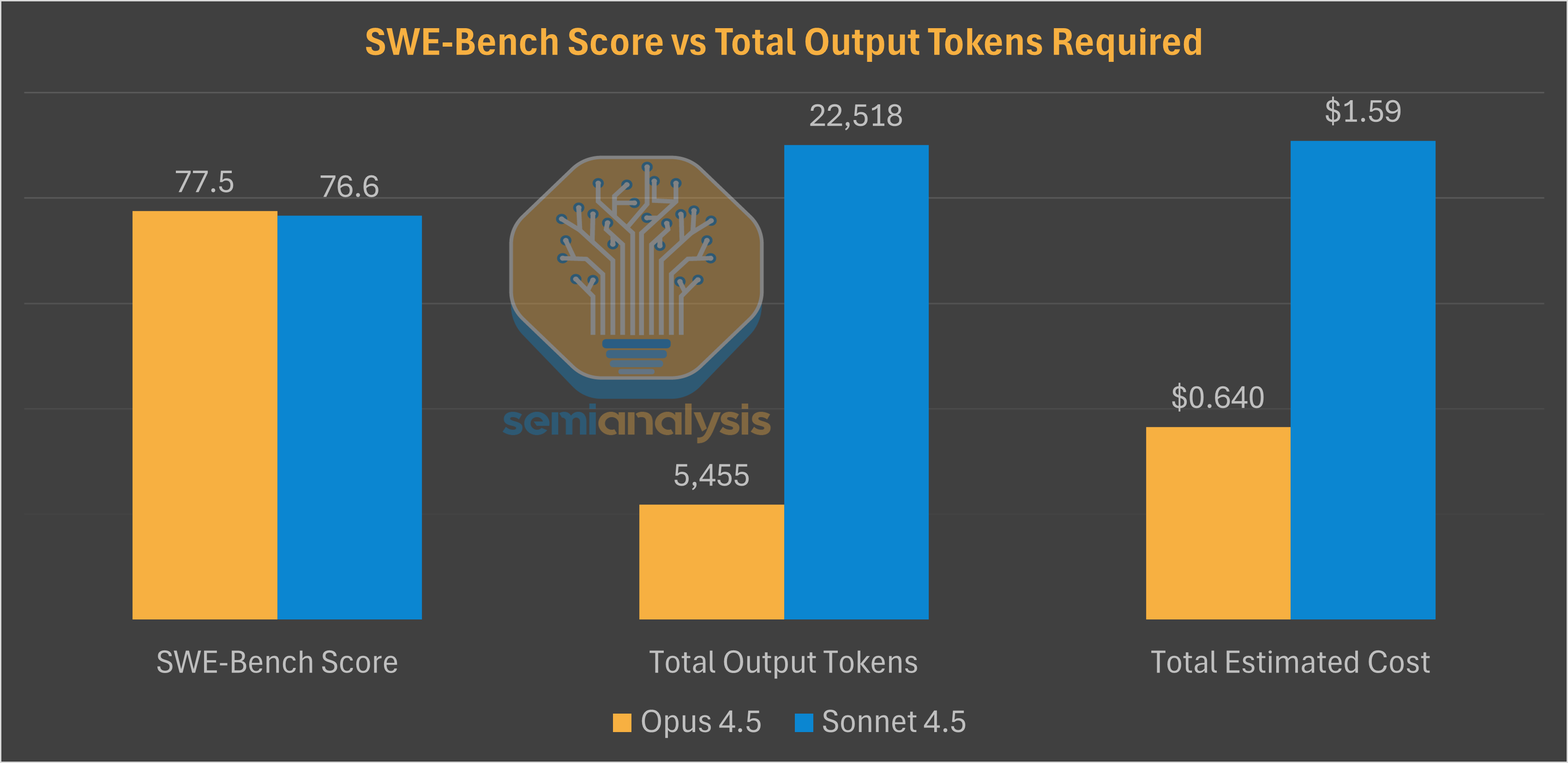
All of this translates into more efficient compute to train and serve a model. Anthropic’s release of Opus 4.5 continued the usual focus on coding, setting a new SWE-Bench record. The main surprise was a ~67% price cut on the API. This price cut paired with the lower verbosity and higher token efficiency of the model compared to Sonnet (76% fewer tokens to match Sonnet’s best score, and 45% fewer to exceed it by 4 points) means Opus 4.5 is the best model for coding use cases and could effectively raise Anthropic’s realized token pricing as Sonnet is over 90% of token mix today.
Google threading the needle on margins
When it comes to pricing for external customers, Google needs to thread the needle to balance their own profitability whilst offering customers a competitive proposition. Our estimate for Anthropic pricing is on the lower end of ranges we’ve heard for external pricing. For a flagship customer such as Anthropic, who will provide valuable input into both the software and hardware roadmap whilst ordering a huge amount of volumes, we’d expect sweetheart pricing. While Nvidia’s eye-watering 4x markup (~75% gross margin) offers a lot of room for pricing flexibility, a good amount of oxygen is sucked away by Broadcom. Broadcom, as the TPU’s co-designer, earns a high margin on the silicon which is the largest component of system BOM. Still, this leaves a lot of room for Google to earn very good acceptable margins.
We can see this from comparing the GCP Anthropic deal to other large GPU-based cloud deals. Note that this is looking at the 600k TPUs that is being rented with the remaining 400k TPU v7 chips being bought upfront by Anthropic.
Under these assumptions, the TPU v7 economics show superior EBIT margins than the other large GPU-based cloud deals we have observed, with only OCI-OpenAI coming close. Even with Broadcom’s margin stack on the chip-level BOM, Google can still eke out far superior margins and returns than much more commoditized GPU deals. This is where the TPU stack allows GCP to be a truly differentiated CSP. Meanwhile someone like Microsoft Azure, whose ASIC program is struggling, is confined to earning more mediocre returns in the mere business of leasing merchant hardware.
TPU system and network architecture
We’ve so far discussed how TPUs compare to Nvidia GPUs, focusing on per chip specs and the shortcomings. Now, let’s get back to the system discussion which is where TPU’s capabilities really start to diverge. One of the most distinctive features of the TPU is its extremely large scale up world size through the ICI protocol. The world size of a TPU pod reaches 9216 Ironwood TPUs, with large pod sizes being a feature of TPUs as early as TPUv2 back in 2017 scaling up to a full 256 1024-chip cluster size. Let’s start at the rack level, the basic building block of each TPU superpod.
Ironwood Rack Architecture
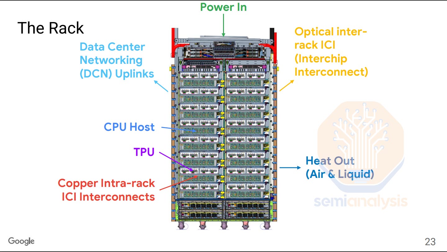
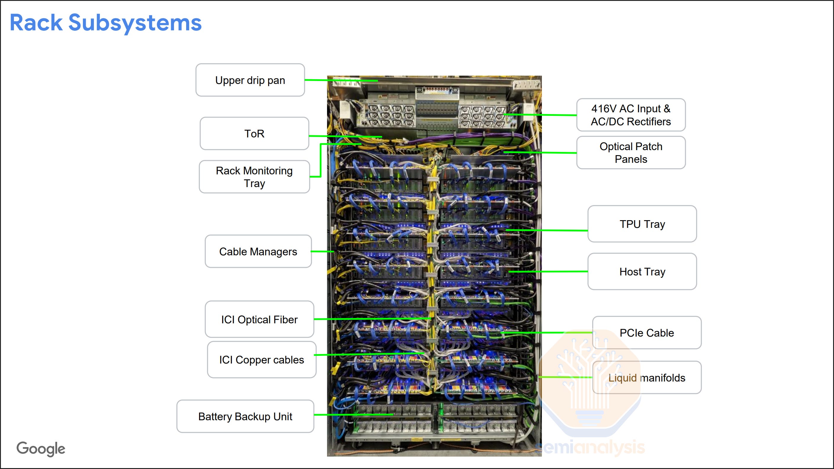
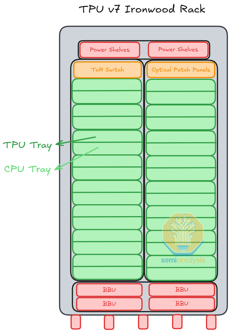
The TPU rack has a similar design over the last couple of generations. Each rack consists of 16 TPU Trays, 16 or 8 Host CPU Trays depending on the cooling configuration, a ToR Switch, power supply units, and BBUs.
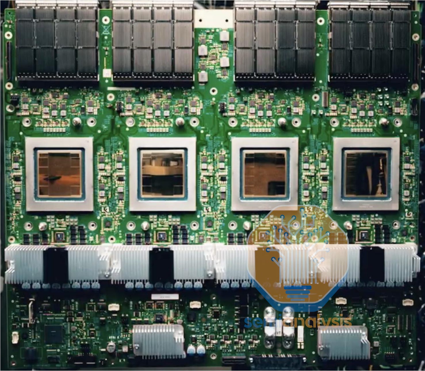
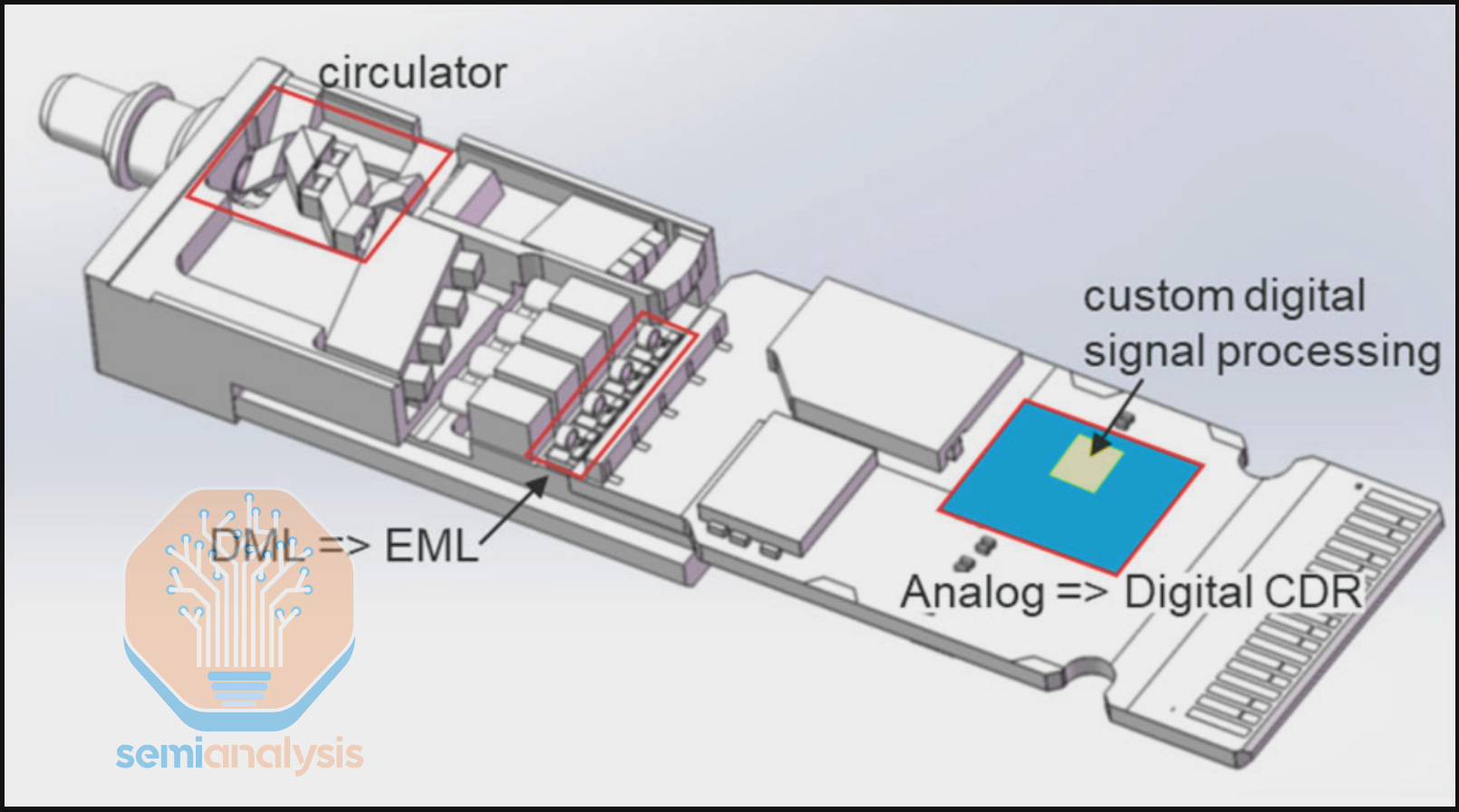
Each TPU tray consists of 1 TPU board with 4 TPU chip packages mounted. Each Ironwood TPU will have 4 OSFP cages for ICI connections and 1 CDFP PCIe cage for the connection to the Host CPU.
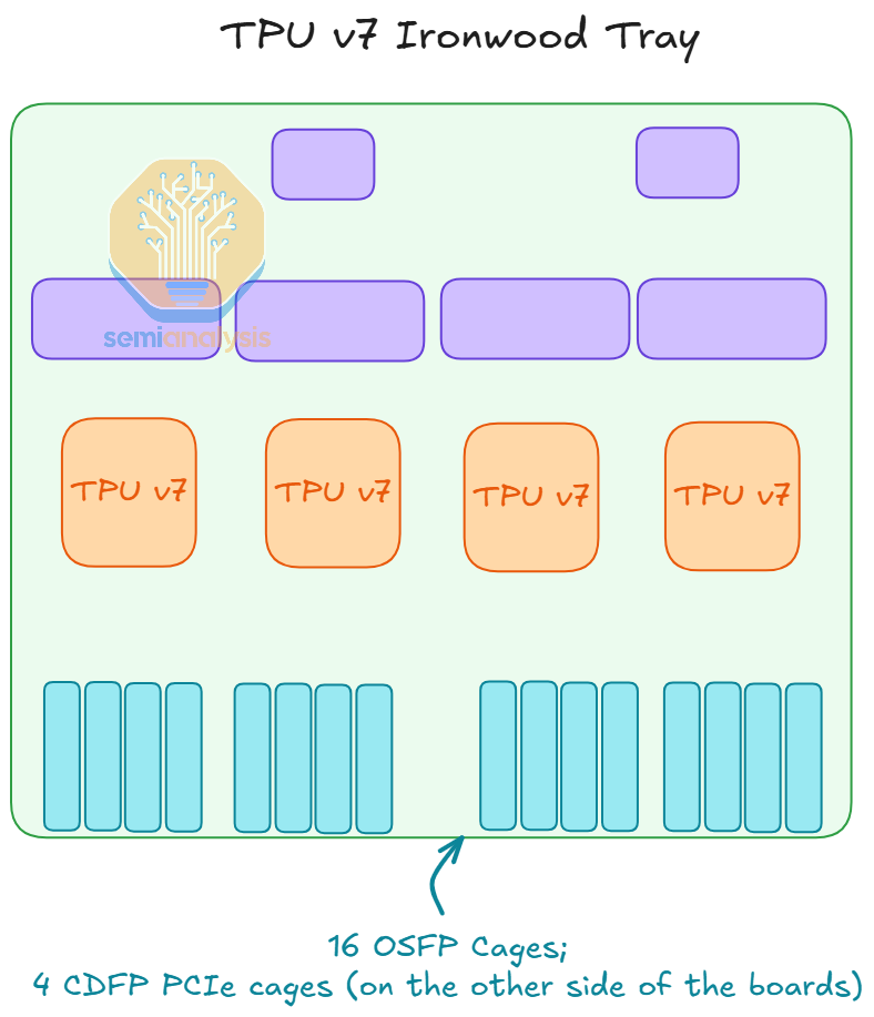
Google has been implementing liquid cooled TPU racks since TPU v3 in 2018, but there are still some TPU generations in between that were designed to be air-cooled. The main difference between the liquid cooled and the air-cooled rack is that the air-cooled rack has 2 TPU trays to 1 host CPU tray ratio while the liquid cooled rack has a 1 to 1 ratio instead.
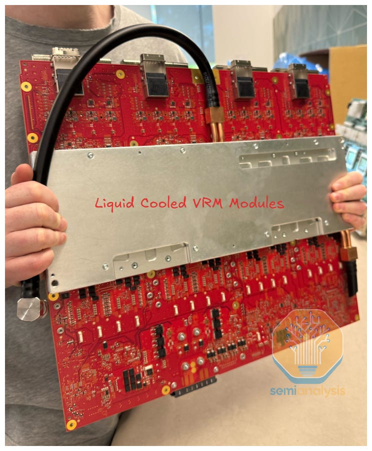
An innovative design of TPU’s liquid cooling is that the flow rate of the coolant is actively controlled by the valves. This enables much more efficient cooling as the flow can be adjusted depending on the amount of workload that each chip has at any given time. Google’s TPU has also long adopted vertical power delivery, in which the VRM modules of the TPUs are on the other side of the PCB board. These VRM modules also require a cold plate for cooling.
Overall, the TPU rack design is much simpler than that of the Nvidia Oberon NVL72 design, which has a much higher density and utilizes a backplane to connect GPUs to scale up switches. The scale up connections between the TPU trays are all over external copper cables or optics, which will be explained in the ICI section below. The connection between the TPU tray and the CPU tray is also over PCIe DAC cable.
Inter-Chip Interconnect (ICI) – The Key to Expanding Scale-Up World Size
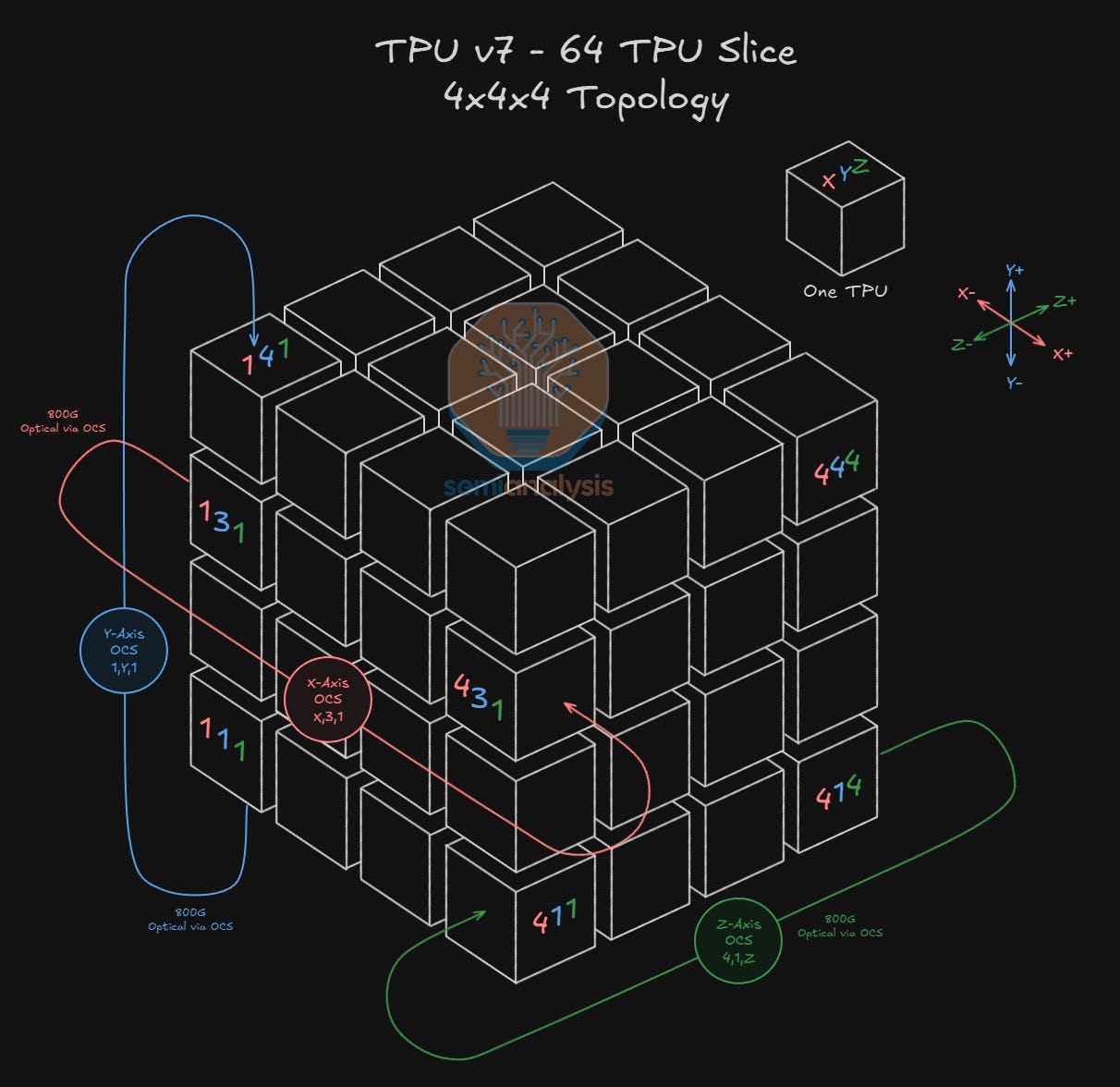
The building block of Google’s ICI scale-up network for TPUv7 is a 4x4x4 3D torus consisting of 64 TPUs. Each 4x4x4 cube of 64 TPUs maps to one physical rack of 64 TPUs. This is an ideal dimension as all 64 TPUs can be connected electrically to each other and still fit in a physical rack.
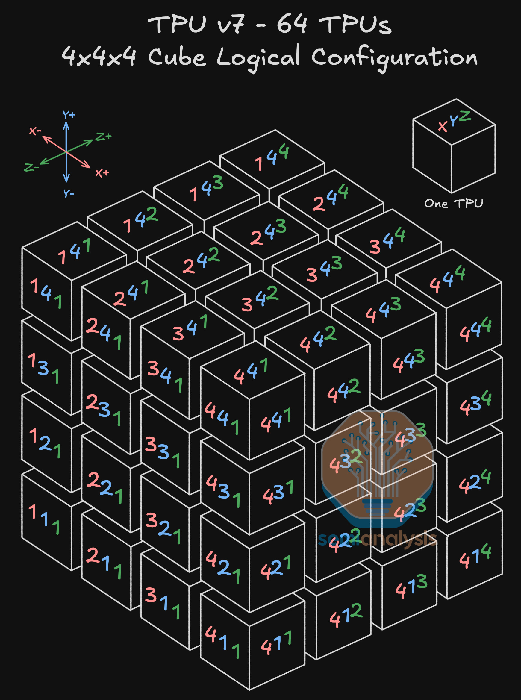
The TPUs are connected to each other in a 3D torus configuration, with each TPU connecting to 6 neighbors total – 2 logically adjacent neighboring TPUs for each of the X, Y and Z axes.
Each TPU is always connected to 2 other TPUs via PCB traces within the compute tray but depending on where the TPU is located within the 4x4x4 cube, it will connect to 4 other neighbors either via Direct Attach Copper (DAC) cables or via an Optical Transceiver.
Connections within the interior of the 4x4x4 cube happen over copper, while connections outside of the 4x4x4 cube (including wrap-around connections back to the other side of the cube as well as connections to neighboring 4x4x4 cubes) will use optical transceivers and OCSs. In the below diagram, we see that as this is a 3D Torus network: TPU 2,3,4 (on the Z+ face) has a wraparound connection back to the opposite Z-axis face to TPU 2,3,1 (on the Z- face) using an 800G optical transceiver and routing through an OCS.
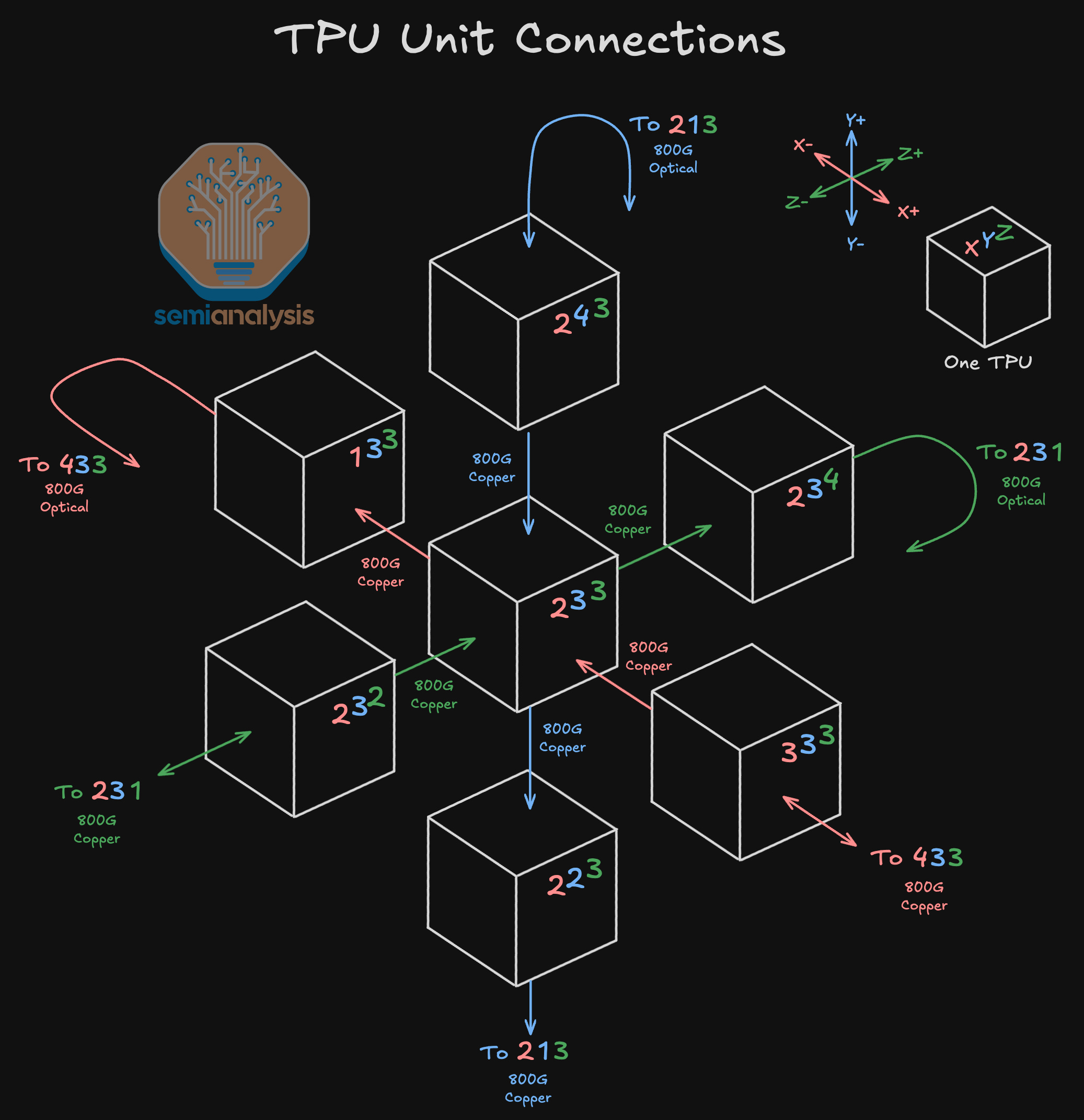
As mentioned above, in addition to the 2 neighboring TPUs that are always connected via PCB traces, TPUs will connect to 4 other neighbors using DACs, transceivers or a mix of both depending on where in the 4x4x4 cube they are.
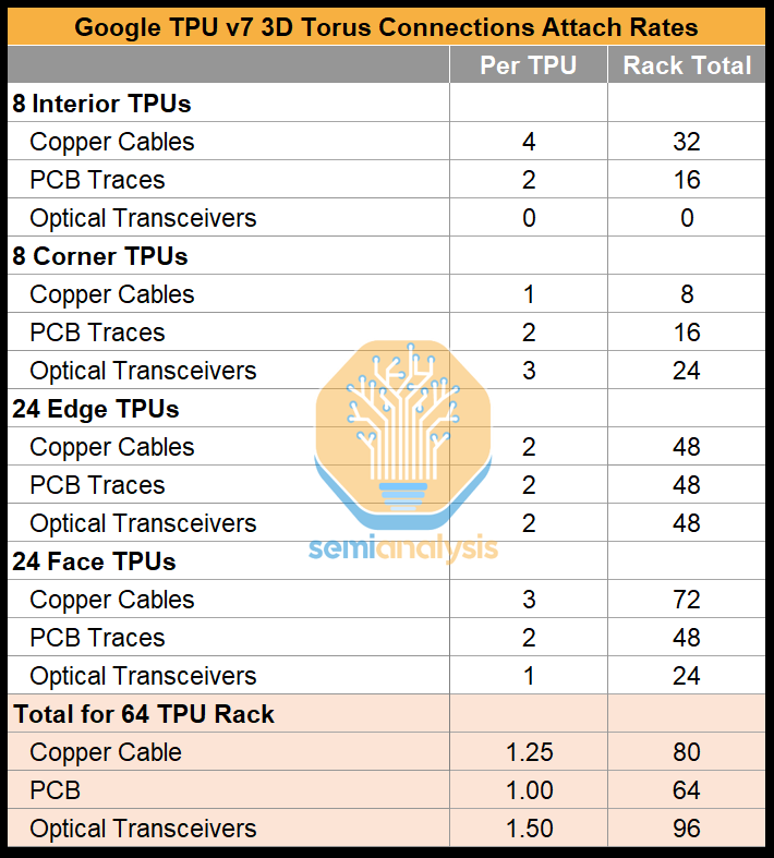
TPUs in the interior of the 4x4x4 cube will connect to the 4 other neighbors exclusively using DACs, TPUs on the face of the cube will connect via 3 DACs and 1 optical transceiver, TPUs on the edge of the cube will connect via 2 optical transceivers and 2 DACs, while TPUs on the corners will connect via 1 DAC and 3 optical transceivers. You can remember how many transceivers a given TPU will use by looking at how many of the TPU’s sides are facing the “outside” of the cube.
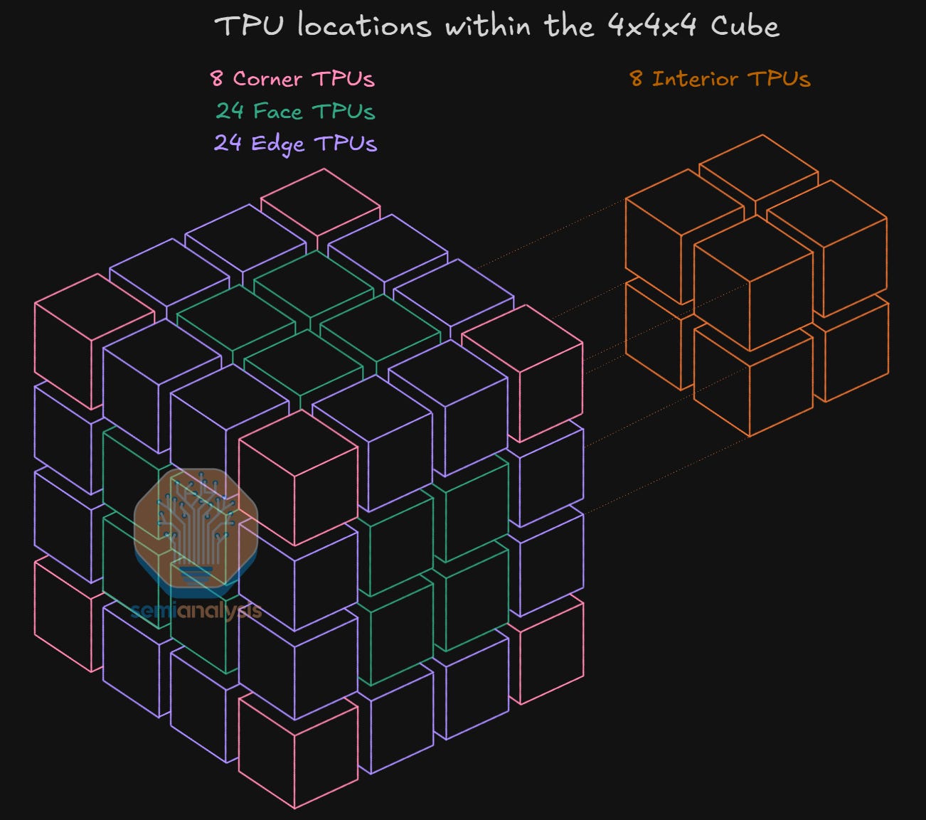
The diagram above, as well as the table below, summarizes the number of respective location types for TPUs and can be used to derive the attach ratio of 1.5 Optical Transceivers per TPU v7. These transceivers connect to Optical Circuit Switches (OCSs) which enable connections between 4x4x4 cubes – more on that in the next section.
Optics for ICI
Google adopts a software-defined networking approach to manage network routes through Optical Circuit Switches (OCSs). An NxN OCS is basically a massive train station with N tracks in and N tracks out. Any train coming in can be transferred to any train coming out, but this has to be reconfigured at the station. Trains cannot be “looped back” or sent back on another N track in, they must be routed only to one of the N tracks out.
The benefit of this approach is that the network can assemble smaller logical TPU slices – for different workloads from the theoretical maximum of 9,216 chips in the ICI network layer. By rerouting ICI paths around faults in the network through slicing a larger cluster, cluster availability improves.
Unlike Electronic Packet Switching (EPS) switches such as an Arista Tomahawk 5 where there is a fixed total bandwidth that is further split into several ports of smaller bandwidth sizes, OCSs allow any bandwidth of optical fiber to be connected to its ports. OCSs is also low latency compared to EPSs because optical signals entering an OCS simply bounce from the input port to the output port. For EPSs, optical signals must be converted to electrical signals when entering the switch – one key reason why an OCS is typically more power efficient than an EPS. An EPS also allows routing of packets from any port to any port, while an OCS only allows you to route an “in” port to any other “out” port only.
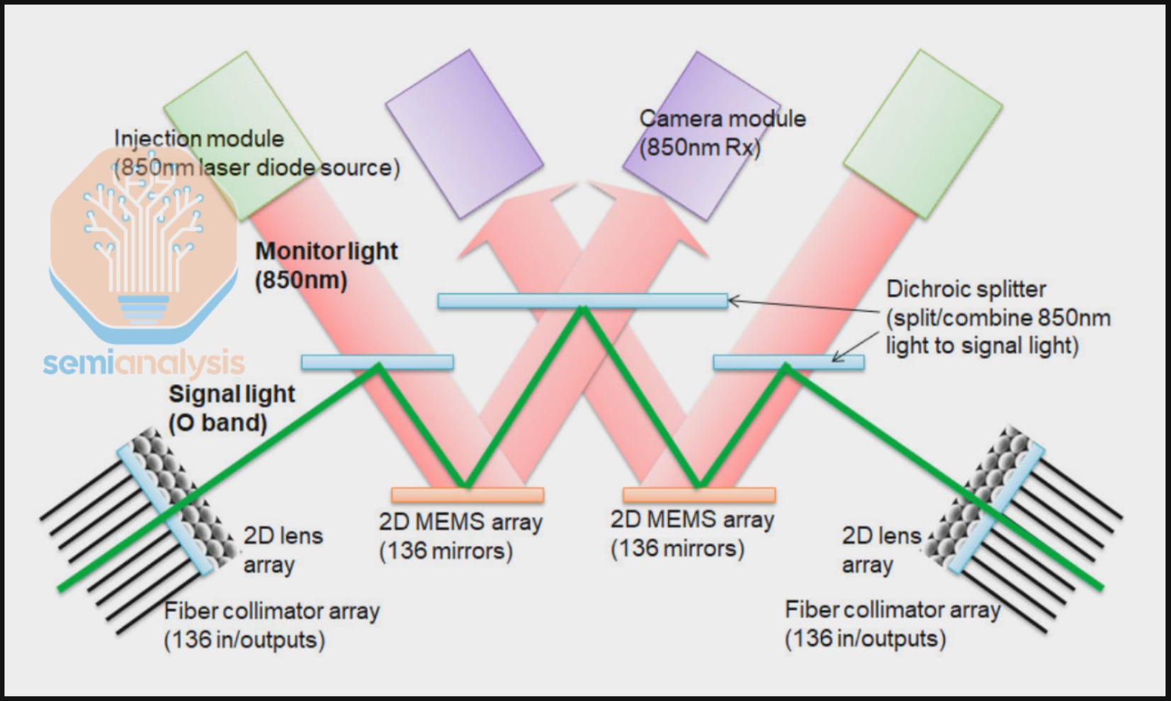
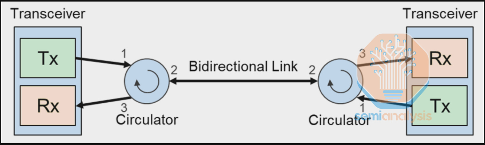
OCS ports only route individual fiber strands. This becomes a challenge for standard duplex transceivers because bandwidth is transmitted over multiple fiber strands, which reduces the effective radix and bandwidth of the OCS. To solve this problem, an FR optical transceiver is used to consolidate all wavelengths onto a single fiber strand to be connected to 1 OCS port. The Apollo Project innovatively achieved this in two steps. First, the 8 wavelengths – 1 wavelength for each 100G lane – are multiplexed through Coarse Wave Division Multiplexing (CWDM8) to transmit 800G over a single fiber pair, instead of 8 fiber pairs. Second, an optical circulator is integrated on the wave division multiplexing (WDM) transceiver to enable full duplex data flow, reducing requirements from 1 fiber pair to only 1 fiber strand.
The circulator forms a bi-directional link by combining the Tx and Rx fiber strands at the transceiver onto a single fiber strand that is sent to the OCS switch.
Connecting Many 64 TPU Cubes Together
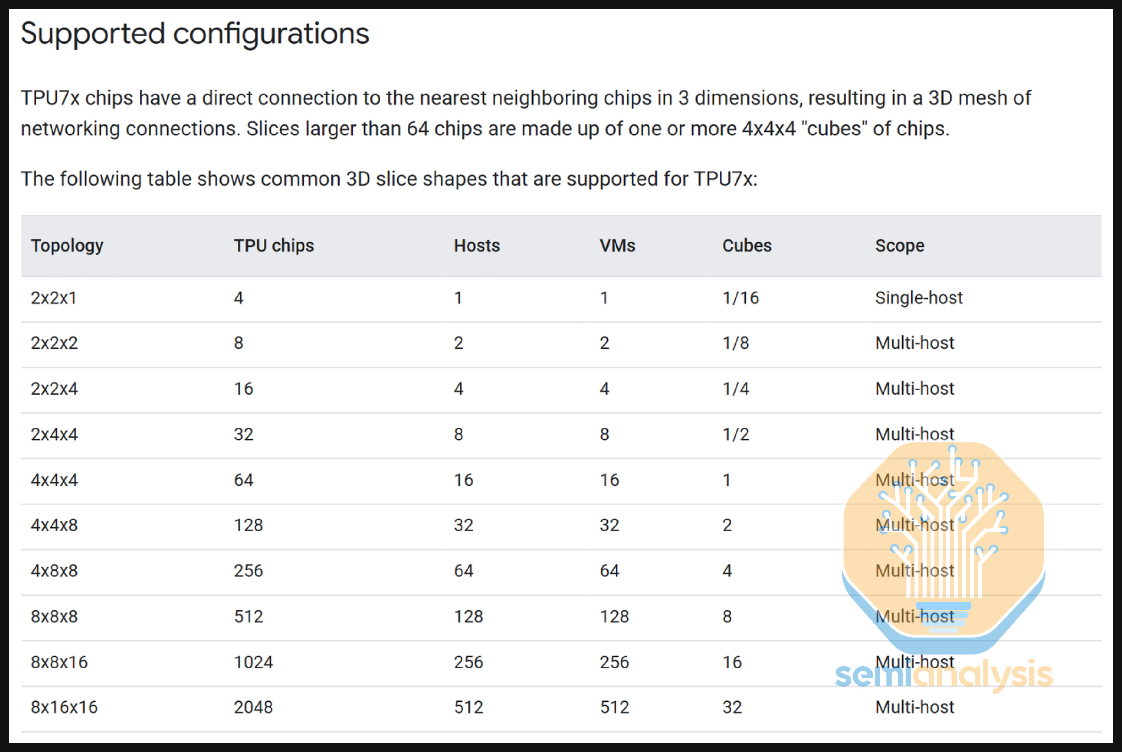
Google’s ICI scale-up network is unique in that it allows the connection of multiple 64 TPU 4x4x4 Cubes together in a 3D torus configuration to create massive world sizes. The TPUv7 has a stated maximum world size of 9,216 TPUs but today, Google supports the configuration of TPUs into multiple different slice sizes of between 4 TPUs all the way up to 2,048 TPUs.
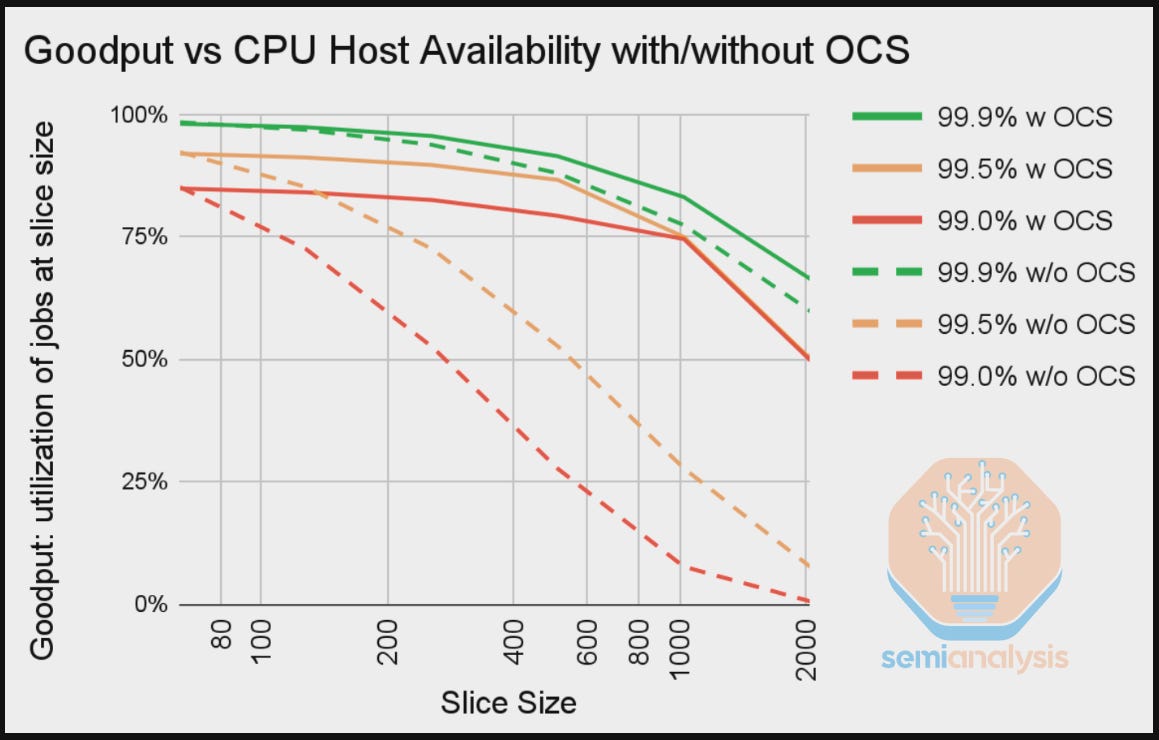
While Google can innovatively achieve an impressive scale-up cluster of 9,216 TPUs, the benefit of running training workloads on incrementally larger block sizes of up to approximately 8,000 TPUs at any point in time decreases. This is because larger block sizes are more prone to failures and disruption, therefore decreasing slice availability, which is defined by the fraction of time in which the ICI cluster is able to form a contiguous 3D torus slice.
For slices that can fit entirely within a 4x4x4 Cube, we can simply carve these slices out of that cube using the copper interconnects within the rack as well as the optical transceivers on the face/edge/corner of the cube to wrap around and complete the 3D Torus if needed.
To see how wraparound and inter-cube connections are made, let’s start by looking at how we would create a 64 TPU slice in a 4x4x4 topography. We can use the unit 4x4x4 cube of 64 TPUs corresponding to one physical 64 TPU rack to build up this topography. All 8 TPUs in the interior of the 4x4x4 cube can fully connect to all 6 neighbors using copper. If a TPU does not have an interior neighbor along a given axis, it will wrap around and connect to a TPU on the opposite side of the cube. For example, TPU 4,1,4 has no interior neighbor in the Z+ direction, so it will use one 800G optical transceiver to connect to an OCS assigned to the Z-axis, with the OCS configured to direct this connection to the Z- side of the cube, connecting to TPU 4,1,1. In the Y- direction, TPU 1,1,1 will use an optical transceiver to connect to a Y-axis OCS to link to the Y+ side of TPU 1,4,1 and so on.
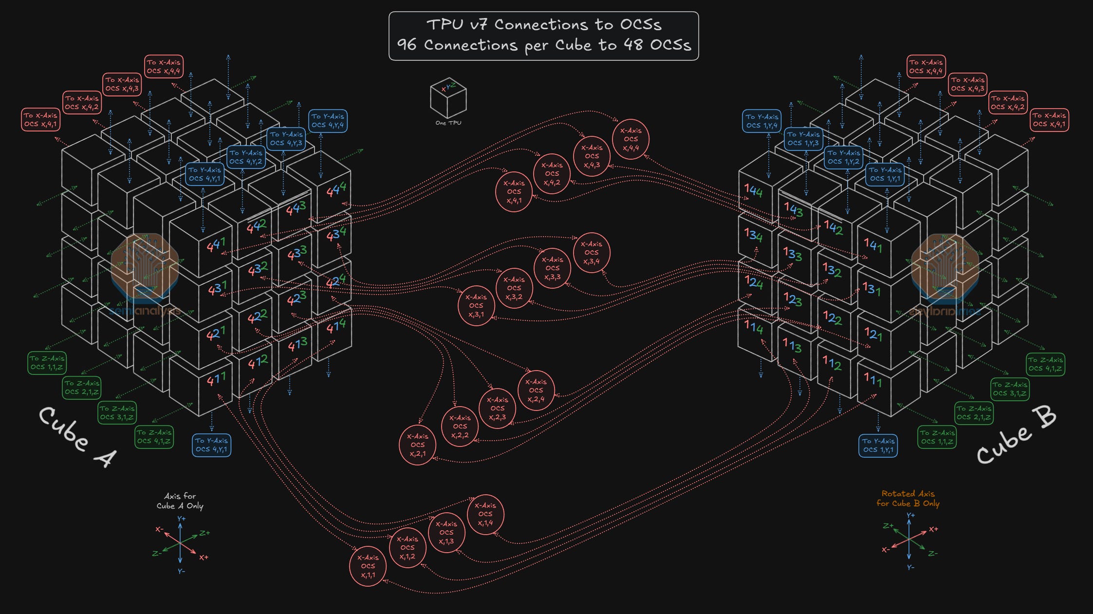
Each face of the 4x4x4 cube will connect via 16 different OCSs – one OCS for each TPU on each face.
For example, in the diagram below, on the X+ face, TPU 4,3,2 connects to the input side of OCS X,3,2. OCS X,3,2’s input side will also connect to the same TPU Index (4,3,2) on the X+ face of all 144 4x4x4 Cubes in the 9,216 TPU cluster. OCS X,3,2’s output side will then connect to the same TPU Index for every single cube in the cluster except this time on the X- face – so it will connect to TPU 1,3,2 on all 144 cubes of the cluster. The diagram below illustrates how all 16 TPUs on the X+ face of Cube A connect via 16 OCSs to 16 TPUs on the X- of Cube B.
These connections allow any “+” face of any cube to connect to the “-“ face of any other cube, enabling complete fungibility of cubes when forming slices.
There are two constraints to briefly point out. First, TPUs of one Index on a given face can never connect directly to a different index – so TPU 4,3,2 could never be configured to connect to TPU 1,2,3. Second, as the OCS essentially acts as a patch panel – TPUs connected on the input side cannot “loop back” to connect to any other TPU that is also connected on the input side of the OCS - as an example, TPU 4,3,2 can never connect to TPU 4,3,3. So – any TPU on the “+” face can never connect to the “+” face of any other cube, and any TPU on the “-” face can never connect to the “-” face of any other cube.
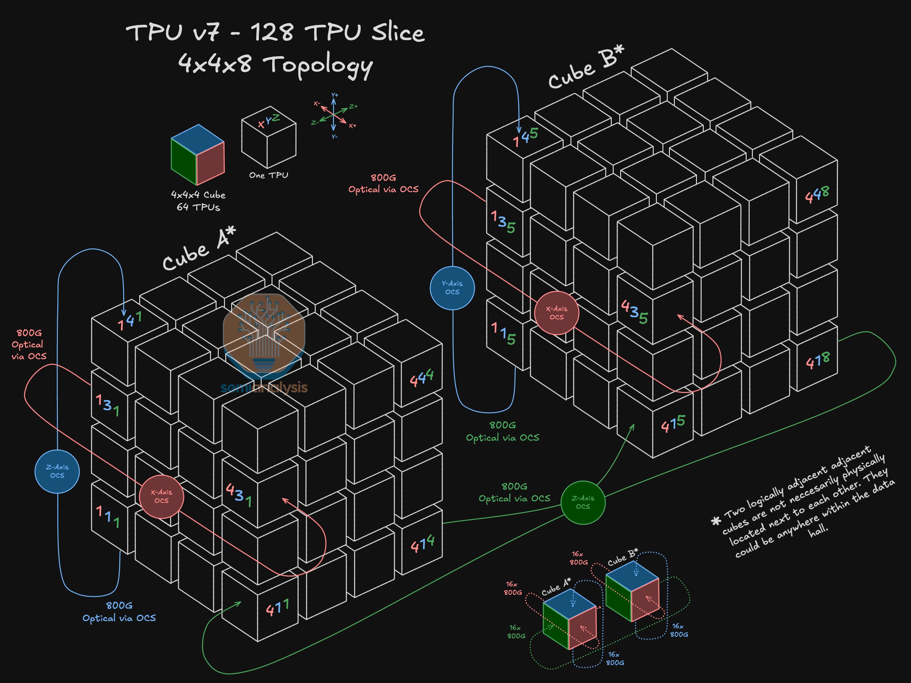
Let’s go larger and see how a 4x4x8 Topography could be set up. In this configuration, we extend the slice by connecting two 64 TPU 4x4x4 cubes along the Z-axis. In this case, the OCS will reconfigure the optical port that TPU 4,1,4 is connected to so that it now connects to TPU 4,1,5 instead of wrapping around back to TPU 4,1,1 as was the case for a standalone 4x4x4 topography. Extending this, we will have 16 optical connections extending from the Z- and Z+ faces of each of the two 4x4x4 TPU cubes, for a total of 64 Fiber strands connected into 16 Z-Axis OCSs.
It is important to remind readers that Cube A and Cube B depicted below are not necessarily physically located next to each other. Instead, they are connected via OCSs and they could each be in completely different locations in the datacenter.
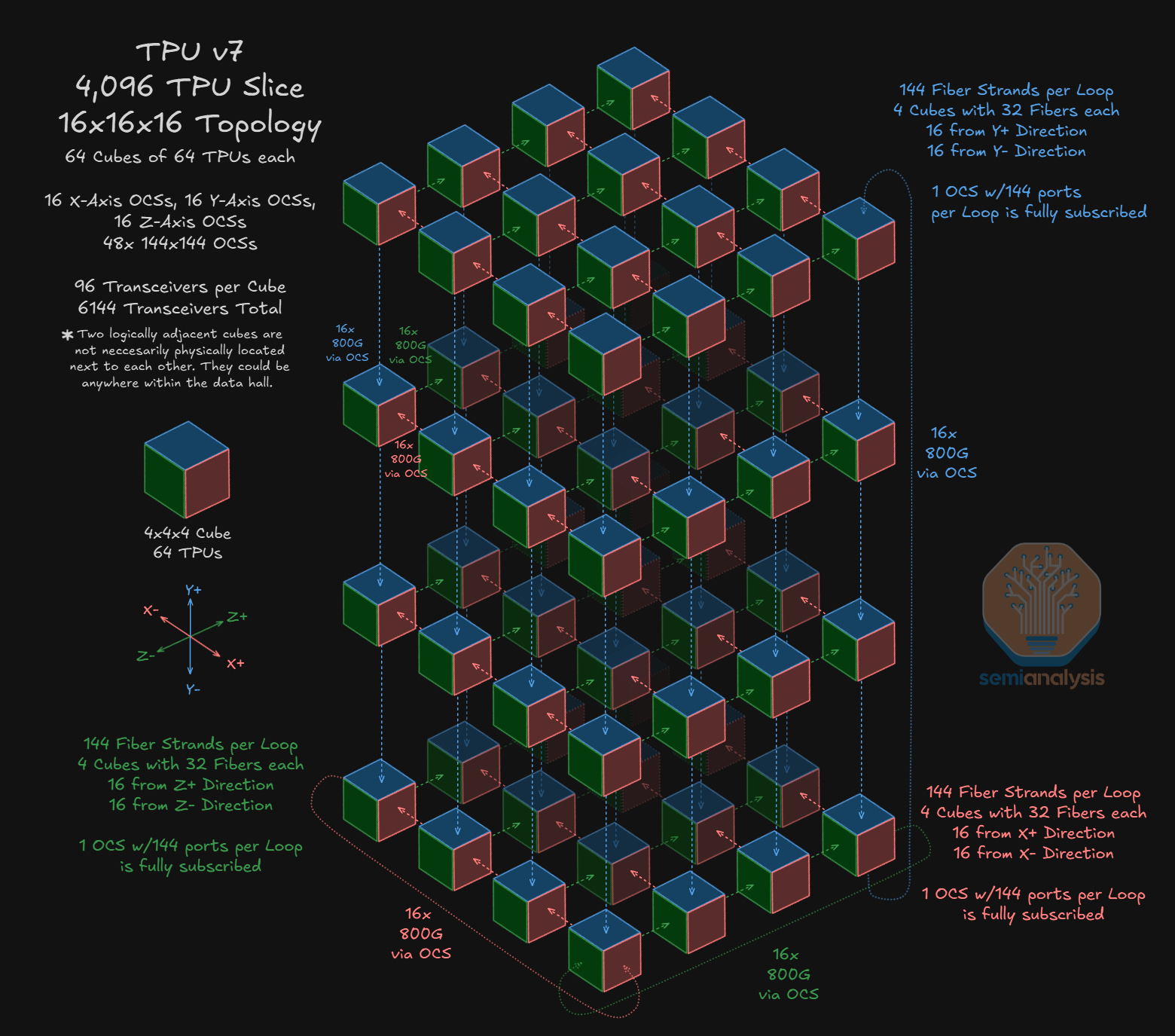
We will now move to a much larger topology – the 16x16x16 topology, which brings us up to 4,096 TPUs. In this topology, we use a total of 48 OCSs to connect 64 Cubes of 64 TPUs each. In the diagram below, each multi-colored cube represents one 64 TPU 4x4x4 cube. Taking the bottom right 4x4x4 cube as an example – this cube is connected to adjacent cubes along the Y-axis via OCSs.
The maximum world size of 9,216 TPUs is built up using 144 4x4x4 cubes requiring 96 optical connections each amounting to a total requirement of 13,824 ports. Dividing this total port requirement by 288 (144 input and 144 output ports on each OCS) means we need 48 144x144 OCSs to support this maximum world size.
Why use Google’s ICI 3D Torus Architecture?
But what is so great about Google’s unique ICI scale-up network – other than all the fancy cube diagrams one can spend countless hours drawing?
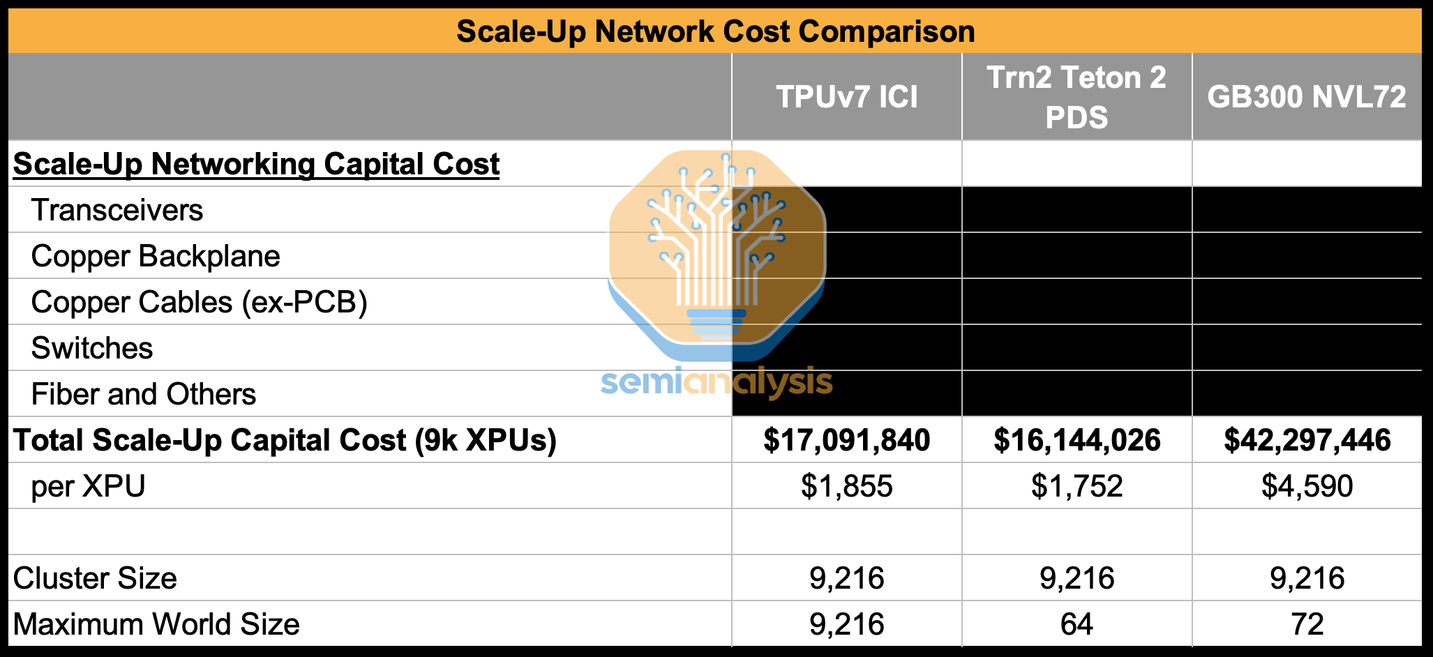
World Size: The most obvious benefit is the very large 9,216 TPU maximum world size that the TPUv7 Ironwood supports. Even though the maximum slice size of 9,216 may rarely be used due to the drawback of diminished goodput, slices of thousands of TPUs can and are commonly used. This is far larger than the 64 or 72 GPU world size that is common in the merchant accelerator market and for other custom silicon providers.
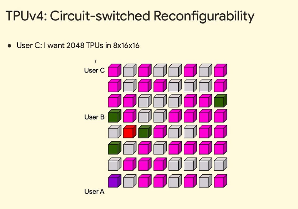
Reconfigurable and Fungibility: The use of OCSs mean that the network topology inherently supports the reconfiguration of network connections to support a high number of different topologies – in theory thousands of topologies. Google’s documentation site lists out 10 different combinations (image earlier in this section), but these are only the most common 3D slice shapes – there are many more available.
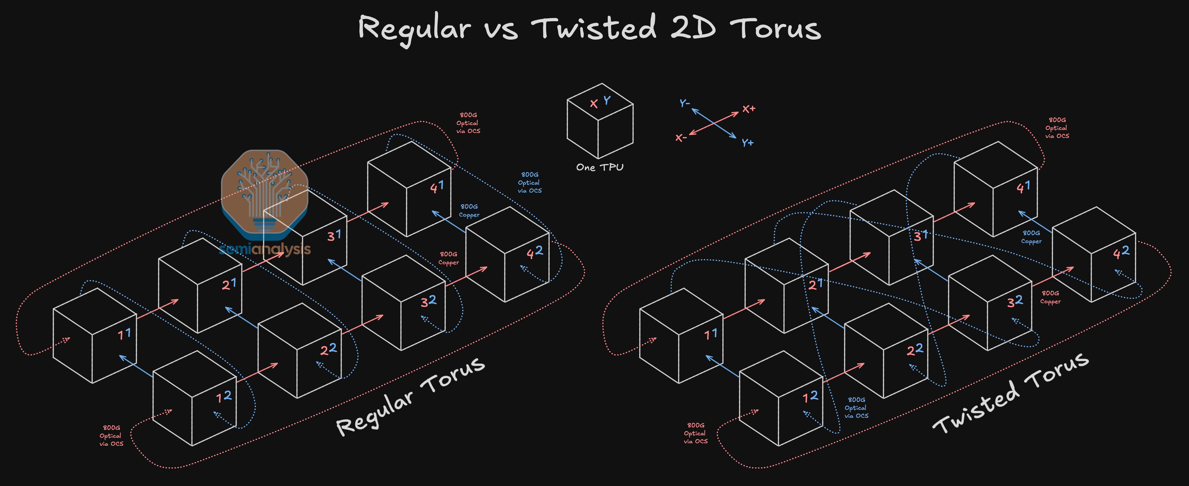
Even slices of the same size can be reconfigured differently. In the simple example of a Twisted 2D Torus diagrammed below, we see how looping across to an index of a different X coordinate instead of an index of the same X coordinate can reduce the worst-case number of hops and the worst-case bisection bandwidth. This can help improve all to all collective throughput. A TPUv7 cluster will twist at the 4x4x4 cube level.
Reconfigurability also opens the door to a broad diversity of parallelisms. In a 64 or 72 GPU world size, different parallelism combinations are generally limited to the factors of 64. When it comes to the ICI scale-up network, the possibilities for implementing topologies to precisely match the combination of data parallelism, tensor parallelism and pipeline parallelism desired are plentiful.
The fact that OCSs allow one to connect any “+” face of any cube to the “-“ face of any other cube means that there is complete fungibility of cubes. Slices can be formed out of any set of cubes. So if there are any faults or change in user demands or usage, this will not obstruct the formation of new topology slices.
Lower Cost: Google’s ICI network has a lower cost than most switched scale-up networks. Though the FR optics used can be slightly expensive due to the use of circulators, the mesh network reduces the overall number of switches and ports that are needed and eliminates cost arising from connections between switches.
Low Latency and Better Locality: The use of direct links between TPUs means that it is possible to achieve much lower latency for TPUs that are physically located close to one another or are reconfigured to connect directly to each other. TPUs that are close to each other also have better data locality.
Datacenter Network (DCN) – Scaling Beyond 9,216 TPUs
The Datacenter Network (DCN) is a network separate to ICI that serves the role of both a typical backend and front-end network. It connects across an even larger domain – 147k TPUs in the case of TPUv7 clusters.
As discussed in our earlier post on Mission Apollo, where Google proposed replacing the Electronic Packet Switch (EPS)-containing spine layer of the traditional “Clos” architecture with Paloma Optical Circuit Switches (OCS), Google’s DCN consists of an optically switched Datacenter Network Interconnect (DCNI) layer that combines several aggregation blocks, each of which connects several 9,216 TPU ICI clusters.
In 2022, Google’s Apollo project proposed a DCN architecture that described using 136x136 OCS switches for TPUv4 pods with a pod size of 4,096 TPUs. OCS switches at the DCNI layer were organized into 4 Apollo zones, each containing a maximum of 8 racks of 8 OCS switches for a total of 256 OCS switches. When it comes to Ironwood, to support up to 147k TPUv7s on the same network, we hypothesize that the number of ports on the OCS will nearly double as opposed to increasing the maximum number of OCS switches.
The diagram below illustrates what an Ironwood DCN network using 32 racks holding 256 300x300 OCS switches could look like. Assuming that there is no oversubscription between the spine layers of each aggregation block, a maximum of 16 ICI pods can be connected in the DCN with 4 aggregation blocks connecting 4 ICI pods each – a total of 147,456 TPUs.
The DCNI layer connects the 4 aggregation blocks – depicted as the top layer in the diagram below. As with ICI, FR Optics are used to connect to the OCSs in order to maximize bandwidth per port on each OCS.
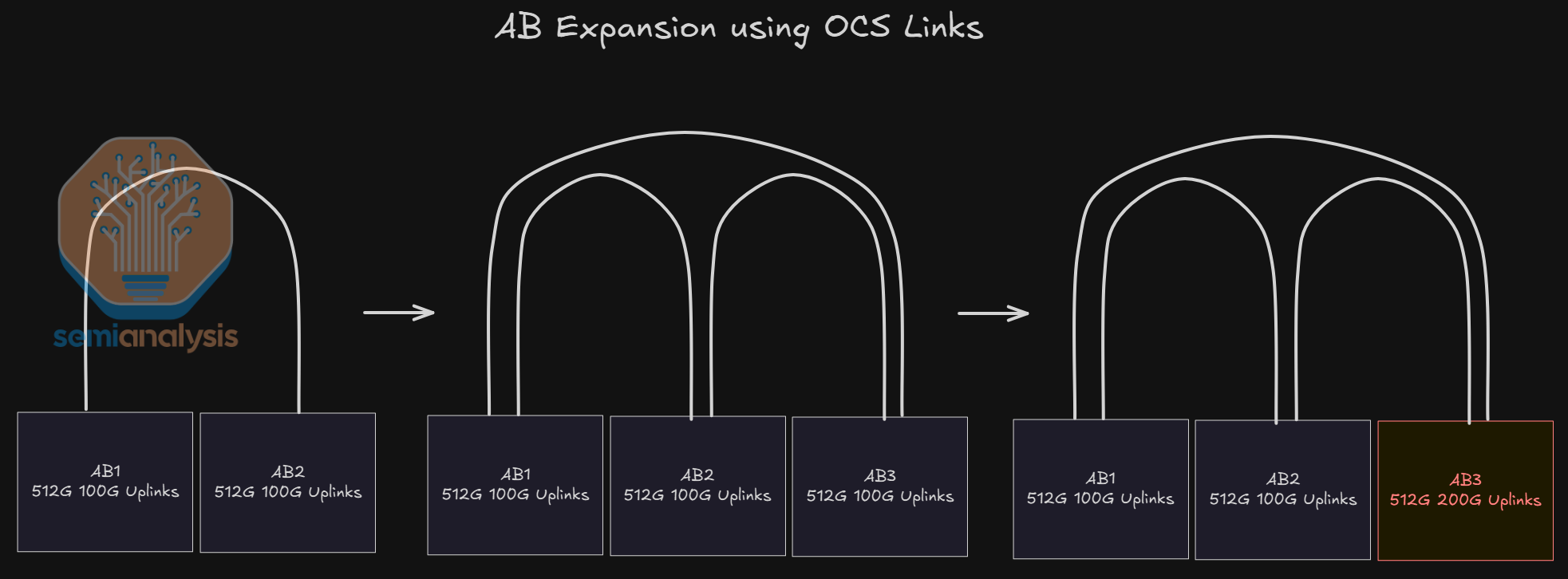
While existing Ironwood clusters may only have 1 or 2 aggregation blocks, Google DCN’s unique architecture allows for new aggregation blocks of TPUs to be added to the network without significant rewiring.
By using OCSs for the DCNI layer, the size of the DCN fabric can be incrementally expanded and the network can be re-striped to support new aggregation blocks. Furthermore, the bandwidth of aggregation blocks can be upgraded without having to change the make-up of the DCN layer. This allows the link speeds of existing aggregation blocks to be refreshed without changing the fundamental architecture of the network itself. The process of fabric expansion cannot go on indefinitely – at significant scale, it becomes unmanageable to rewire the network.
TPU Software Strategy – Another Monumental Shift
Traditionally, TPU software and hardware teams have been internal-facing. This comes with advantages such as the absence of pressure by marketing teams to inflate stated theoretical FLOPs.
Another advantage of being only internal facing is that the TPU teams heavily prioritized internal feature requests & optimizing internal workloads. The disadvantage is that they did not care much about external customers or workloads. The number of external developers in the TPU ecosystem is way lower than in the CUDA ecosystem. This is one of the main weaknesses of the TPU as it is with all non-Nvidia accelerators.
Google has since revised their software strategy for externally-facing customers and has already made major changes to their TPU team’s KPIs and how they approach contributing to the AI/ML ecosystem. There are 2 major changes that we will discuss:
Massive engineering effort on PyTorch TPU “native” support
Massive engineering effort on vLLM/SGLang TPU support
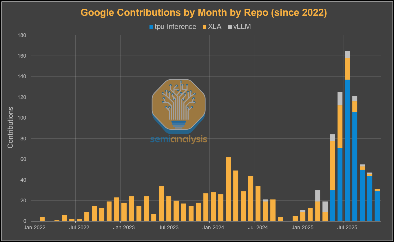
The externalization strategy is clear to see by looking at the number of contributions from various TPU software repos by Google. We can see a noticeable increase in vLLM contributions starting from March. Then from May, the “tpu-inference” repo was created which is the official vLLM TPU unified back-end, and since then there has been a flurry of activity.
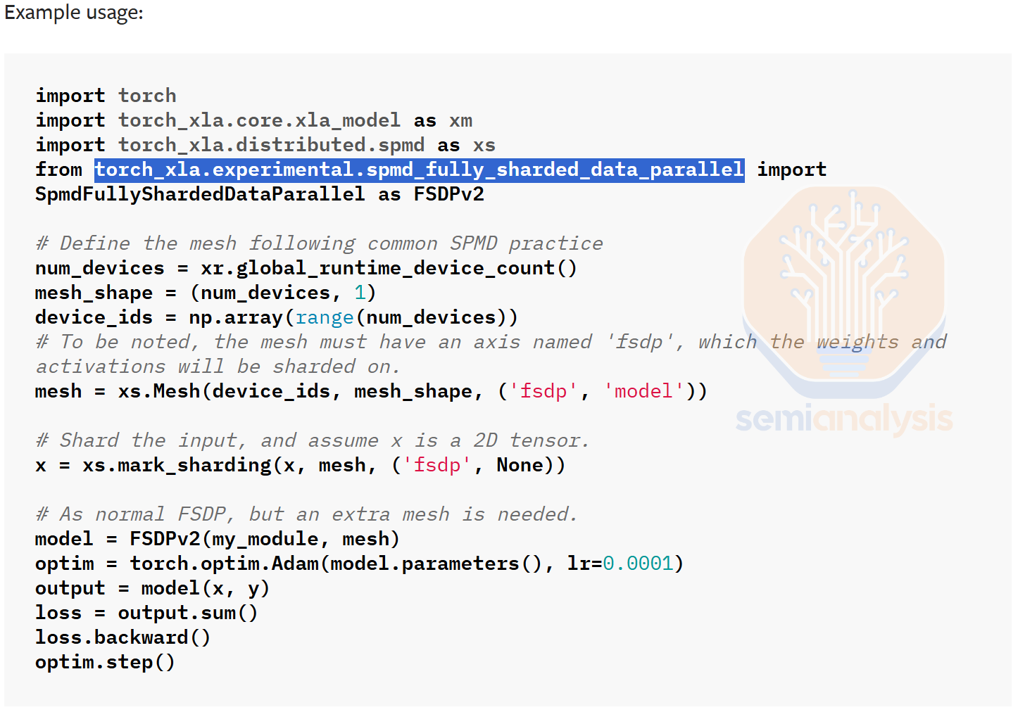
Traditionally, Google only had first class support on the Jax/XLA:TPU stack (and TensorFlow/TF-Mesh RIP), but treated PyTorch on TPU as second class citizen. It relied on lazy tensor graph capture through PyTorch/XLA instead of having a first-class eager execution mode. Furthermore, it did not support PyTorch native distributed APIs (torch.distributed.*) or support PyTorch native parallelism APIs (DTensor, FSDP2, DDP, etc), but relied on weird out of tree XLA SPMD APIs (torch_xla.experimental.spmd_fsdp, torch_xla.distributed.spmd, etc.). This has led to a subpar non-native experience for external users that are used to the native PyTorch CUDA backend on GPUs and trying to switch to TPUs.
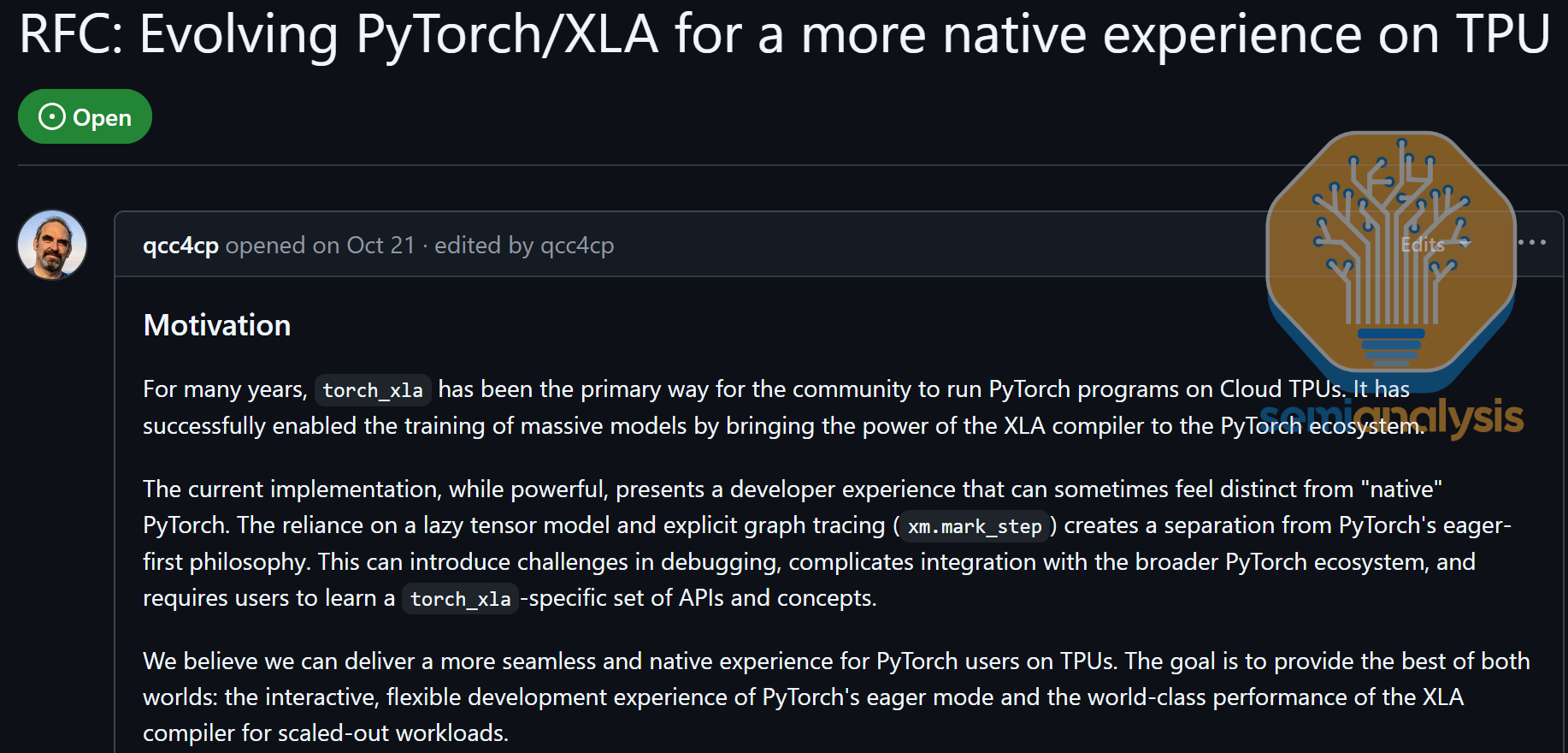
In October, Google’s “Captain Awesome” Robert Hundt quietly announced in the XLA repo that they will be moving away from a non-native lazy tensor backend towards a “native” TPU PyTorch backend that will support eager execution by default & integration with torch.compile & DTensor & torch.distributed APIs, etc. They will be doing this through the use of PrivateUse1 TorchDispatch key. This will mainly be done for Meta who has renewed interest in buying TPUs & does not want to move to JAX. It will also make it for people that enjoy PyTorch and do not like JAX to use TPUs too.
Previously from 2020 to 2023, heavily used by a couple of teams at Meta FAIR used PyTorch XLA on TPUs but it was not widely adopted thus Meta leadership ended up cancelling the contracts in 2023. PyTorch XLA on TPUs is not a fun experience. The Meta FAIR GCP TPUs back then were even run using SLURM and not anything typical you would find on TPU stack like GKE/Xmanager/borg/etc.
This new PyTorch <> TPU will create a smoother transition for ML scientists that are used to PyTorch on GPUs to switch to PyTorch on TPUs and take advantage of the higher performance per TCO on TPUs.
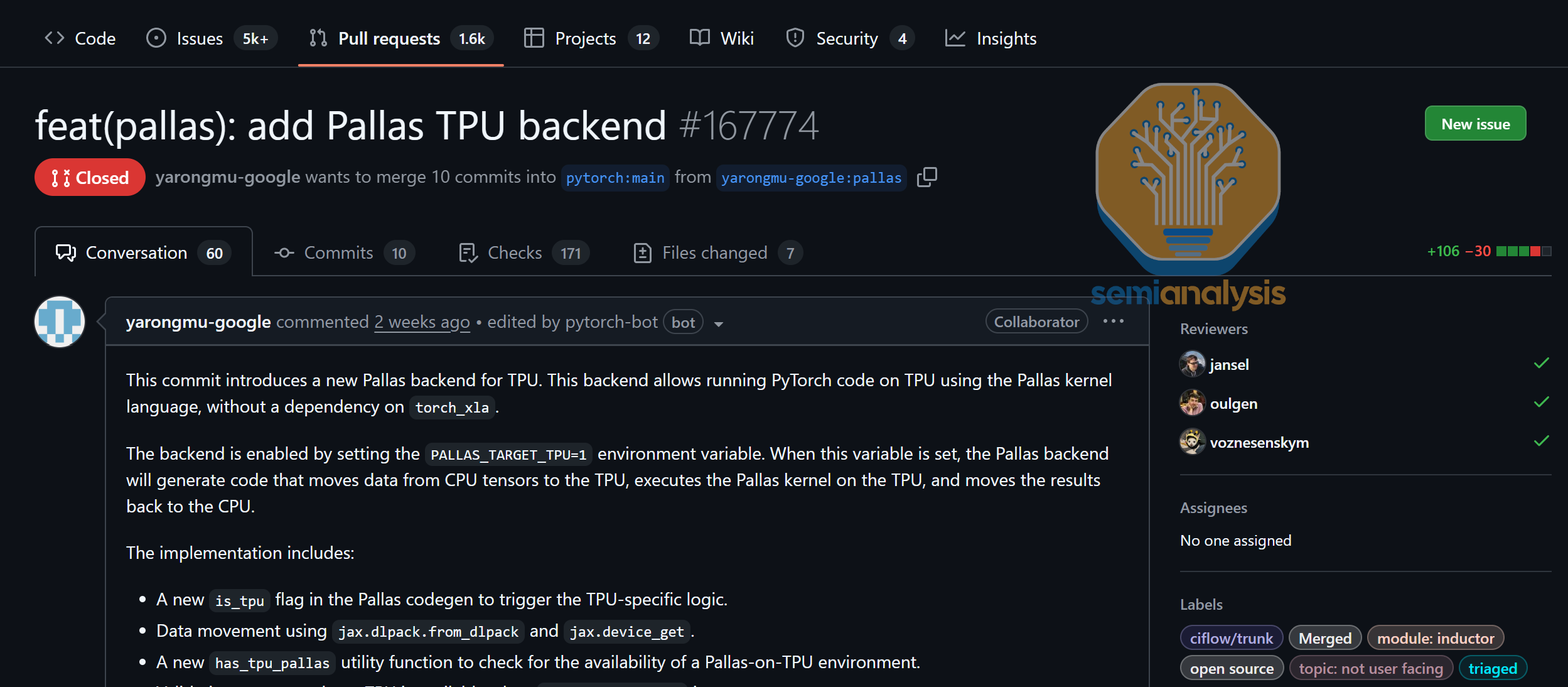
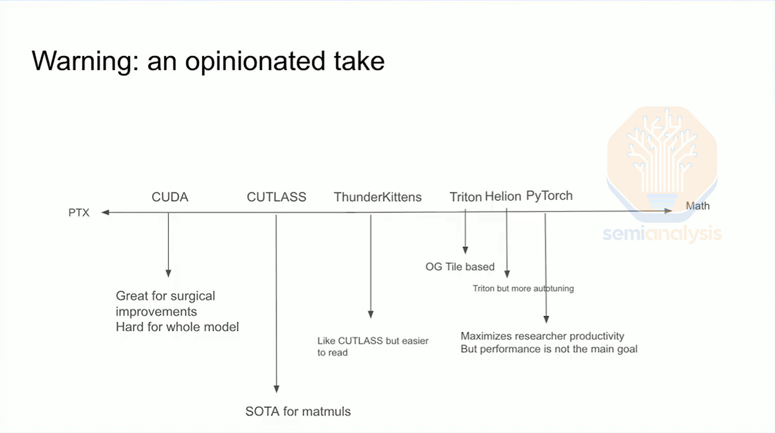
Pallas is the kernel authoring language for writing custom kernels for TPU (similar to cuTile or Triton or CuTe-DSL). Meta & Google have also started work on supporting Pallas kernels as a codegen target for the Torch Dynamo/Inductor compile stack. This will allow for native TPU integration with PyTorch’s native torch.compile API & allow for end users to register custom pallas ops into PyTorch.
In addition to the core in tree PyTorch native APIs, there is also work behind the scenes on integrating TPU pallas kernel language as a codegen target for Helion. You can think of Helion as a higher-level language for writing decently performing kernels in a high level language. Users can think about Helion as a low level Aten operators rather than as high level Triton/Pallas due to its similarity matching much closer to the Native PyTorch Aten ops.
Another area where the CUDA ecosystem is supreme is for open ecosystem inference. Historically, vLLM & SGLang support CUDA as first class (as ROCm as 2nd class citizen). Now Google wants in to the vLLM & SGlang open inference ecosystem and have announced beta TPU v5p/v6e support for vLLM & SGLang through a very “unique” integration.
vLLM& SGLang currently does this by lowering the PyTorch modelling code into JAX and taking advantage of the existing mature JAX TPU compilation flow. In the future once PyTorch XLA RFC #9684 (aka native TPU PyTorch backend) gets implemented, vLLM & SGLang plan on evaluating whether to switch to using that instead of translating modelling from PyTorch to JAX through TorchAX.
Google & vLLM claim that this lowering to jax path does not require any changes to the PyTorch modelling code but given how few models vLLM TPU supports so far, we doubt this is true.
Furthermore, Google has open-sourced & integrated some of their TPU kernels into vLLM such as a TPU optimized paged attention kernels, compute-comms overlapped GEMM kernels & a couple other quantized matmul kernels. They do not yet have MLA-friendly TPU kernels. It would be interesting to see once Inductor Pallas TPU codegen integration is more mature, whether it is possible to integrate kernel fusion & pattern matching into the existing vLLM PassManager. SGLang is also looking into implementing an torch.compile PassManager to make managing kernel fusions for many models more maintainable.
For Ragged Paged Attention v3, TPU handles it quite differently from vLLM GPU. vLLM manages KV cache with a technique similar to virtual memory and paging. However, this technique requires fetching dynamic addresses and performing scatter operations, something TPUs don’t support well. As a result, TPU kernels leverage fine-grained operation pipelining. Specifically, TPU’s page attention kernel prefetches query and KV blocks for the next sequence, so the memory loading is overlapped with computation.
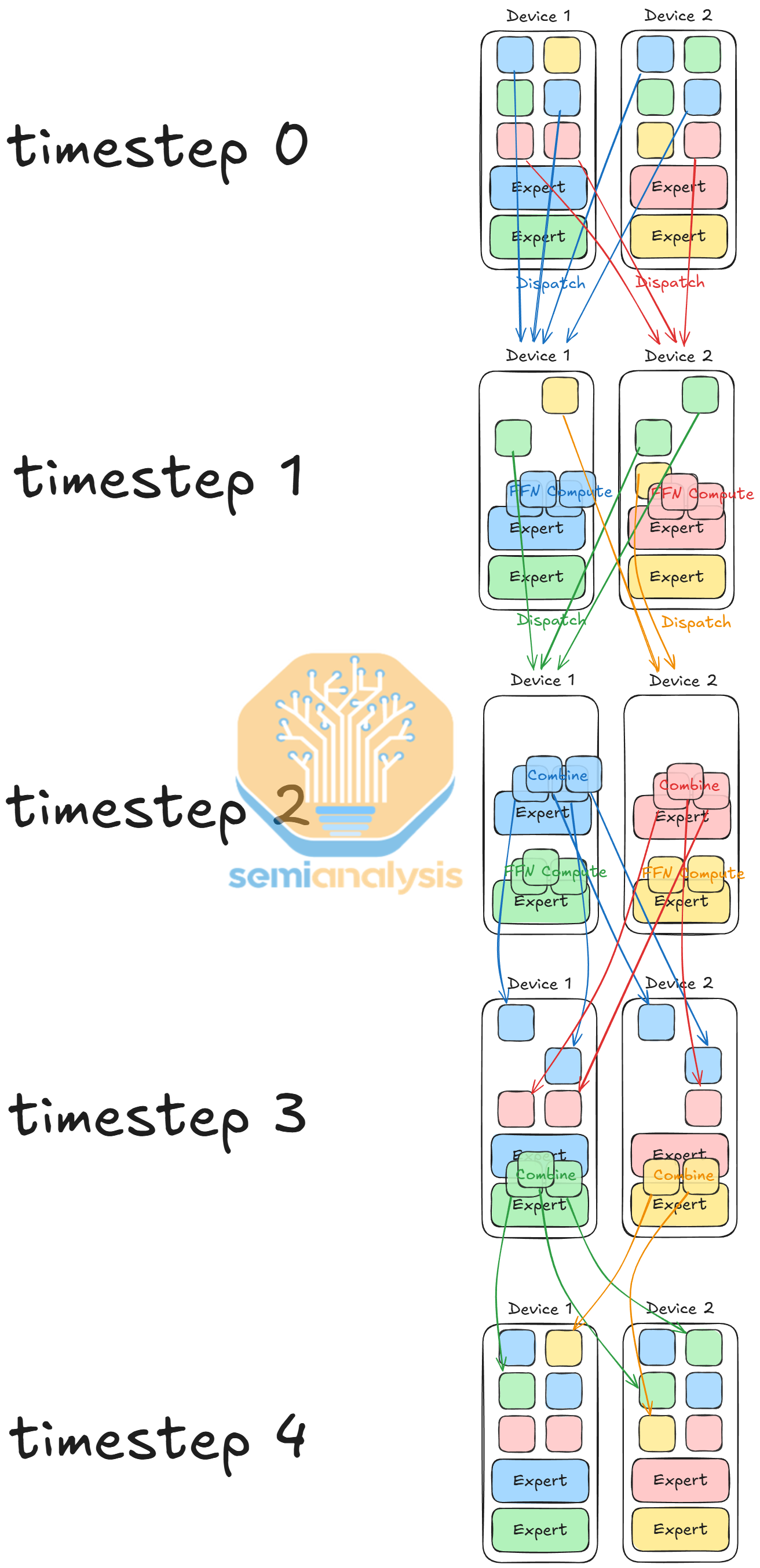
In the existing vLLM MoE kernel, we sort tokens by expert ID, dispatch tokens to the devices with the corresponding experts, perform group matrix multiplication, and combine tokens from experts back to original devices. However, the kernel performs poorly for two reasons: TPUs are slow at performing sorting operations, and the kernel is unable to overlap communication with computation.
To work around this issue, Google developers designed all-fused MoE. All-fused MoE dispatches tokens for one expert per device at a time while overlapping MoE dispatch & MoE combine communications & avoiding sorting tokens by expert ID. With all-fused MoE, the Google engineer reported 3 - 4x speedup over existing kernels.
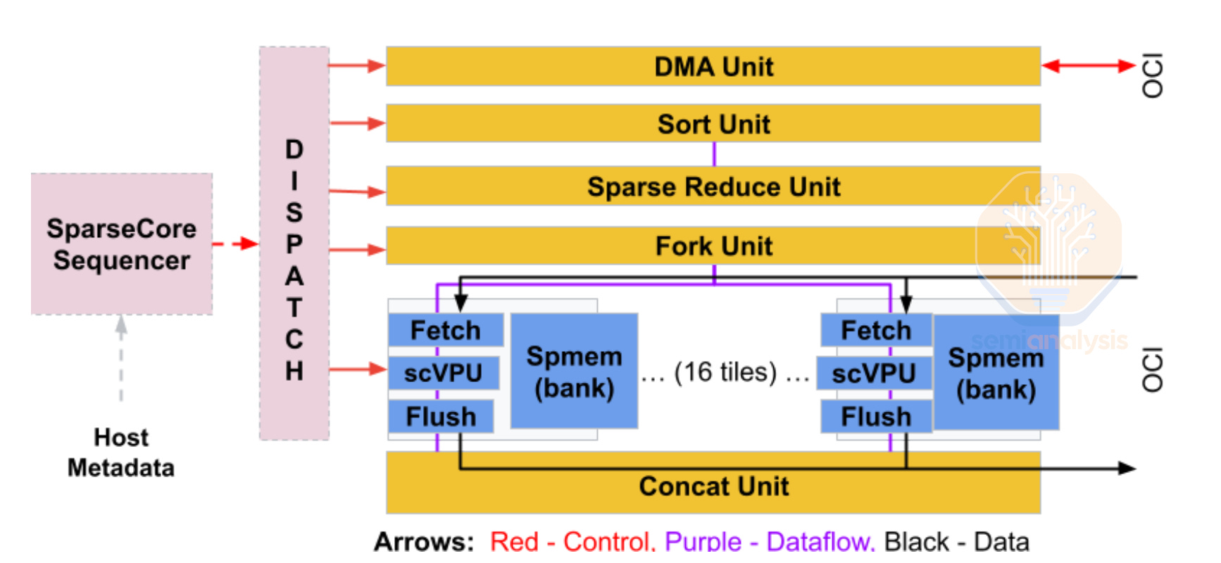
Furthermore, another hardware unit in TPUs is the SparseCore (SC) used to accelerate embedding lookups and updates. SC comes with a scalar subcore SparseCore Sequencer (SCS) and multiple vector subcores SparseCore Tiles (SCT). SCT supports local and remote direct memory access at a more fine-grained 4-byte or 32-byte granularity, compared to TPU TensorCore’s 512-byte loads. This enables SC to perform gather/scatter operations and ICI communications while overlapping with TensorCore operations.
At JAX DevLabs, we learned that programmability of SparseCore is a work in progress. We can expect Mosaic, the TPU custom kernel compiler, to compile in an MPMD fashion, where SCS and SCT executes different kernels, and different SparseCores can run different programs. We suspect once the programmability catches up, TPU MoE kernels would be able to perform dispatch and combine operations in a similar way as GPUs, instead of dispatching by expert IDs.
In terms of disaggregated prefill decode, which we described in depth in our AMD 2.0 post, Google has experimental support on vLLM for single host disagg PD, not they do not support multi-host wideEP disagg prefill or MTP yet. These inference optimizations are critical to lower the TCO per million tokens and increase the perf per dollar and perf per watt. Furthermore, they have not yet integrated TPU vLLM inference support into popular RL frameworks like VERL, etc. Google is slowly moving in the correct direction in terms of how they approach the open AI/ML ecosystem especially for their “native” TPU backend.
vLLM TPU Benchmarks are not relevant yet
This week, there was an new inference benchmark on TPUv6e that dropped claiming that TPUv6e has 5x worst performance per dollar than NVIDIA GPUs. We disagree mainly due to 2 reasons. First of all, this is benchmark is on vLLM on TPUs which was only released an couple month ago thus does not yet have optimized performance. Google internal Gemini workloads & Anthropic workloads work on an internal custom inference stack that has better perf per TCO than NVIDIA GPUs.
Secondly, Aritifical Analysis’s cost per million tokens is using the list price of $2.7/hr/chip for TPUv6e. No major customers of TPUs is paying anywhere close to that much for TPUv6e given the BOM is a tiny fraction of the H100. As everyone knows, most clouds have an high ball list price such that their account sales executives can do “car salesman” tactics and give massive discounts so that the customer thinks they are getting a good deal. The SemiAnalysis AI TCO Model tracks the acutal market rental price of TPUs across all the various contract lengths (1 month, 1 year, 3 years, etc).

Critical Missing Piece of TPU Software Stategy
One part where Google is still approaching their software strategy incorrectly is with their XLA graph compiler & networking libraries & TPU runtime is still not open sourced nor well documented. This has led to frustrated users across the spectrum from advanced users to the average user of not being able to debug what is going wrong with their code. Furthermore their MegaScale codebase for multi-pod training is not open source either.
We strongly believe that in order to accelerate the adoption, Google should open source it and the increased user adoption will outweigh all the software IP they will make public & free. Just like how PyTorch or Linux being open sourced rapidly increased adoption, open sourcing XLA:TPU & TPU runtime & networking libs will rapidly accelerated this too.
What does this mean for Nvidia?
Now that Google has gotten their act together on TPU and is selling them externally for people to put in their own datacenters, what are the implications on Nvidia’s business? Does Nvidia finally have a legitimate competitor that will put its market share and margins at threat? Behind the paywall, we will share our thoughts on what this means for Nvidia as well as reveal more about the TPU roadmap.