

Cerebras — Faster Tokens Please
OpenAI and AWS Partnerships, Tokenomics Explainer, Architecture Deep Dive, Datacenter Ramp, Technical Roadmap
It’s been nearly 5 years since Dylan wrote a dedicated article about Cerebras in June of 2021 for the newsletter. He shipped 4 articles in 2 days! How times have changed.
One of the other things that has changed is Cerebras’s fortunes. With the arrival of fast tokens on the mainstage and a 750MW compute deal with OpenAI notched, Cerebras is feeling ready for the scrutiny of public markets. Up until just 6 months ago, we felt that the Wafer Scale Engine, despite its bold innovations, had some technical weaknesses that were too hard to cover up. Thus, the continued popularity of HBM-based accelerators such as GPU and TPU. The strengths of Cerebras (namely: speed), have been overlooked for years in favor of total throughput. But now, with frontier labs releasing fast, priority, standard and batch tiers of the same model weights, the world has revealed their preference for fast tokens with their wallets. This brings Cerebras’s strengths to the fore and is the key reason why OpenAI is willing to fork over tens of billions of dollars for Cerebras compute.
Demand is so strong it’s making everyone look good.
Today, on the verge of Cerebras’s IPO, and because we love the wafer, we are shipping an article that is as long as 4 normal articles. Inside, we will dive deep on:
Fast inference
WSE-3, Cerebras’ unique wafer-scale chip
CS-3, Cerebras’ system, with its unique architecture
Provide a BOM cost analysis
Explain when and how the wafer wins for fast inference
Describe some of the wafer’s limitations, showing tradeoffs
For paid subscribers we also show the economics of the huge OAI Inference deal that has changed the company’s fortunes and share our insights on how far along Cerebras is in becoming a neocloud (i.e. securing the 750MW they need by 2028 for OpenAI). Furthermore, we will talk about Cerebras’ future plans of hybrid bonding an wafer scale optical transceiver onto their WSE compute engine, which they claim they are pursuing strictly for the love the game as it is not needed for LLM inference, but is needed for HPC boomer workloads. The HPC customers whom NVIDIA has effectively abandoned after reducing FP64 native hardware on their GPUs to basically nothing.
The Need for Speed
Fast inference has arrived.
While SemiAnalysis has historically been an SRAM machine hater, all this changed when Nvidia licensiquihired Groq in December 2025. Clearly Jensen saw at least $20B of value, and he was proven right just a couple months later when we hit the Claude Code Inflection Point. Now, the wafer is here to stay.
Many (including Andrej Karpathy) previously believed that raw intelligence/capabilities mattered far more than speed, but our revealed preferences ended up proving that there are times when the opposite is true. Past a certain threshold of intelligence, developers prefer faster tokens to smarter tokens. And in a world where AI is involved in almost every aspect of your workflow, the speed at which tokens are generated can be the bottleneck to “flow state”, i.e. how much productive work is completed.
Opus 4.6 fast mode famously charges 6x the price for 2.5x the interactivity (though its now under 2x faster, see chart below). In April, 80% of our AI spend (which peaked at $10M annualized) was on Opus 4.6 fast. When Opus 4.7 came out, many of our engineers refused to switch over because it didn’t include fast mode. Notably, this is the first time we’ve ever decided to forgo frontier intelligence in exchange for faster tokens (and at a significant price premium too!).
As an aside, Opus 4.6 fast has become an increasingly worse deal as of late. Standard Opus 4.6 interactivity in Claude Code is consistently around 40 tps (tokens per second). Opus 4.6 fast used to deliver > 100 tps, fulfilling the 2.5 faster guarantee. But it recently degraded to ~70 tps (only 1.75x faster). We recently worked with our friends at OpenRouter to gather this data on the two operating modes of Claude Opus.
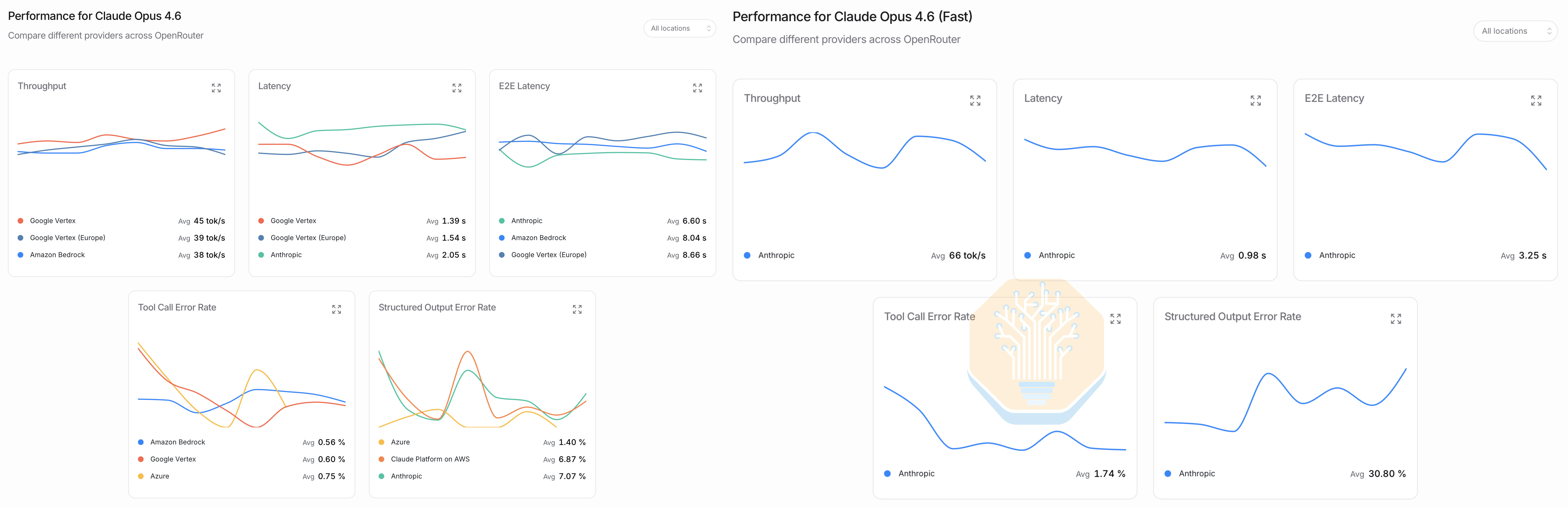
We believe Opus 4.6 Fast is Anthropic’s highest margin SKU and a big reason for their explosion in ARR this year. However, we’ll see if this remains true given the slower speeds, delayed 4.7 support, and upcoming Mythos release. For in-depth details on OpenAI/Anthropic revenue broken down by model, see our Tokenomics Model.
The Throughput-Interactivity Frontier
To fully explain the architectural decisions Cerebras has made with their wafer scale chip, we first need to revisit inference fundamentals.
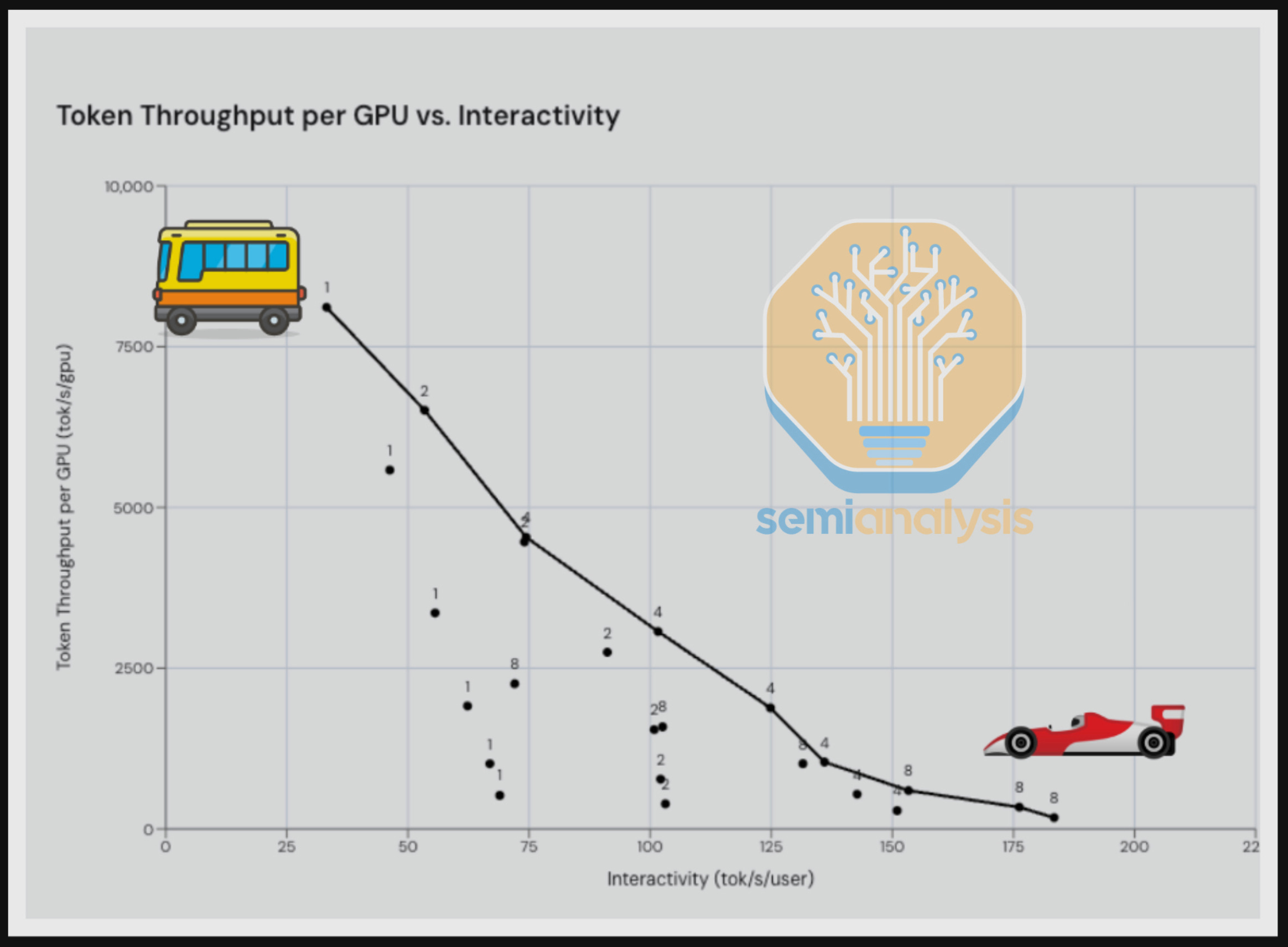
As Jensen repeatedly emphasized during this year’s GTC, throughput (tokens/sec/gpu) vs interactivity (tokens/sec/user) is the fundamental trade-off for inference. In our original InferenceX writeup, we described it as a bus vs a Ferrari: you can choose to serve lots of users slowly, a single user quickly, or anything in between.
Of course, users are also willing to pay more money for higher interactivity, so it’s currently unclear exactly which spot along the pareto frontier maximizes overall revenue and profitability of inference for a given model provider. In reality, providers are currently deploying multiple options in an attempt to capture the entire market. Fast mode, priority mode, batch pricing, and specific model architectures are all experiments from OpenAI and Anthropic to find the optimal combination for their user base.
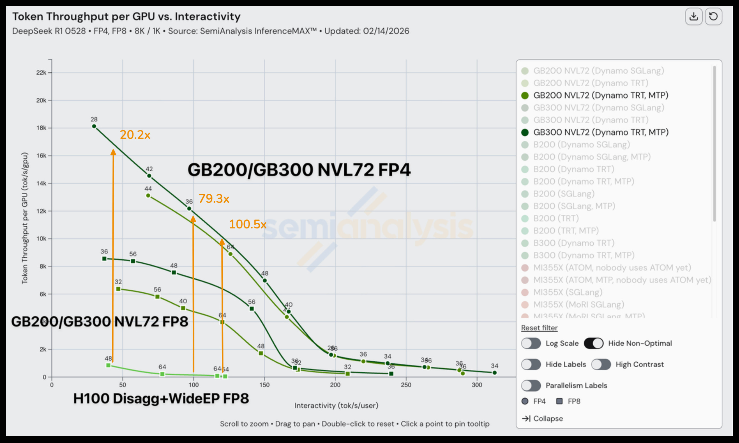
Manipulating batch size (or “concurrency”, the number of users you serve simultaneously) is the primary way to move along the curve given the same hardware. This is the beauty of InferenceX. Whereas most other public inference benchmark only considers a single workload at a single interactivity level, InferenceX builds the entire pareto frontier across 3 different input/output sequence length combos for all the top open-source models. This allows you to make charts like the following, which shows that GB300 NVL72 achieves 20x more throughput than H100s at low interactivity (40 tps) and 100x more throughput at high interactivity (120 tps).
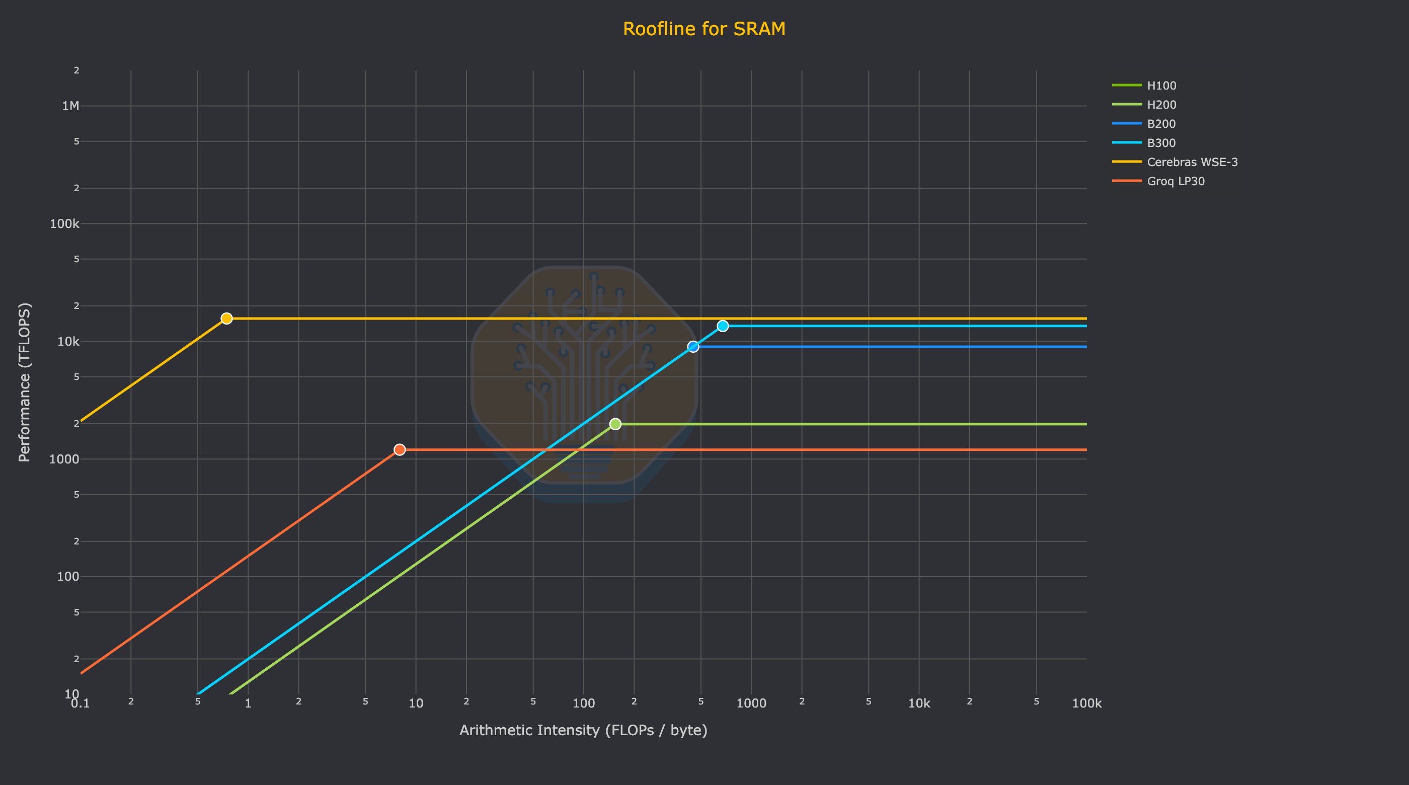
Alternatively, you can move along the frontier by changing the underlying hardware. This is the promise of SRAM machines like Cerebras and Groq. Their extremely high memory bandwidth allows them to increase throughput at high interactivity, and in the extreme case, achieve interactivity levels that are simply impossible for HBM-based accelerators. Cerebras offers speeds in the thousands of tokens per second, which is literally off the chart compared to the accelerators we benchmark in InferenceX.
In a world where people are willing to pay more for faster tokens, SRAM machines look quite attractive as they let you both (a) serve more users concurrently at premium speed (pushing the frontier “up”) and (b) serve some users at even faster, more expensive speeds (extending the frontier to the right).
The Wafer-Scale Engine
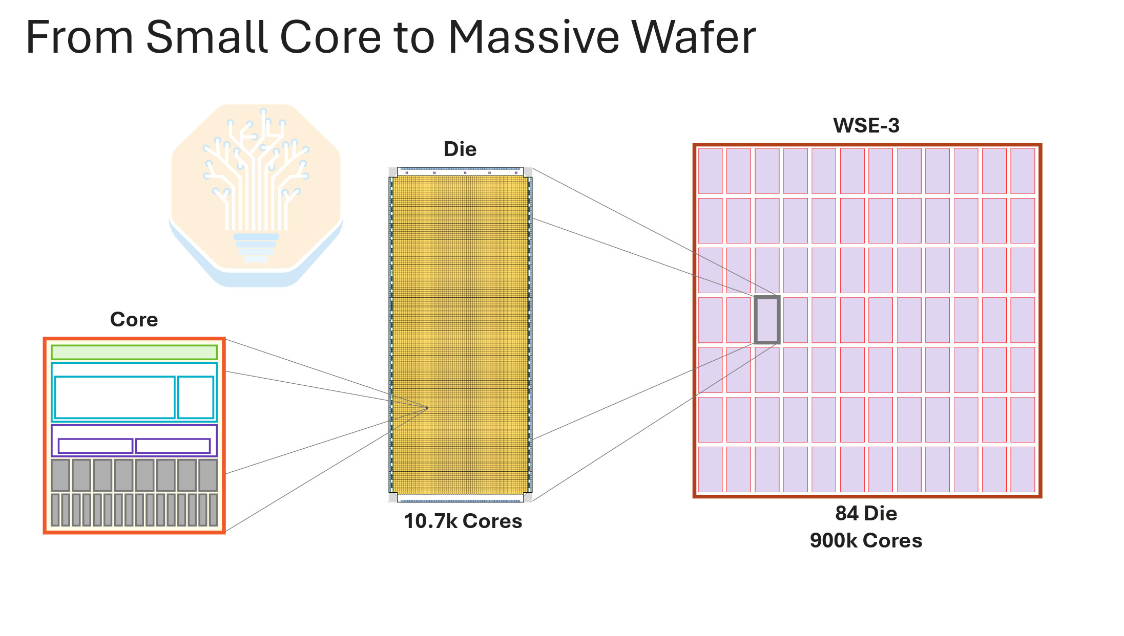
Cerebras’s fundamental bet has been to go beyond the reticle limit for a single piece of silicon. Instead of splitting a wafer into multiple chips, the goal is to make the entire wafer a chip. This clever scaling was to address a whole host of problems incurred by the slowdown of Moore’s law and the hard constraint of silicon being no larger than 858mm2; the size of a single reticle pattern in mask-based lithography. This single wafer-sized chip is called their Wafer Scale Engine (WSE).
The WSE is a 12 x 7 grid of 84 identical steppings/die on a whole wafer that forms one piece of silicon. Each wafer or chip has a large pool of very fast SRAM. 50% of silicon area is dedicated to SRAM cells with the remaining 50% consisting of compute cores. The key innovation is having both the silicon and memory on one piece of silicon instead of interconnecting multiple different chips together. This saves power, latency, and cost of moving data off-silicon or off-package.
“Traditional” GPUs and XPUs need advanced packaging and networking to achieve greater levels of aggregate compute and memory, which incurs costs in terms of power, speed and more networking equipment. While not a like-for-like comparison, Cerebras compares its on-wafer dataflow speeds to Nvidia’s off-package scale-up bandwidth based on the assumption that data can stay on the WSE whereas GPU data needs to move off-package.
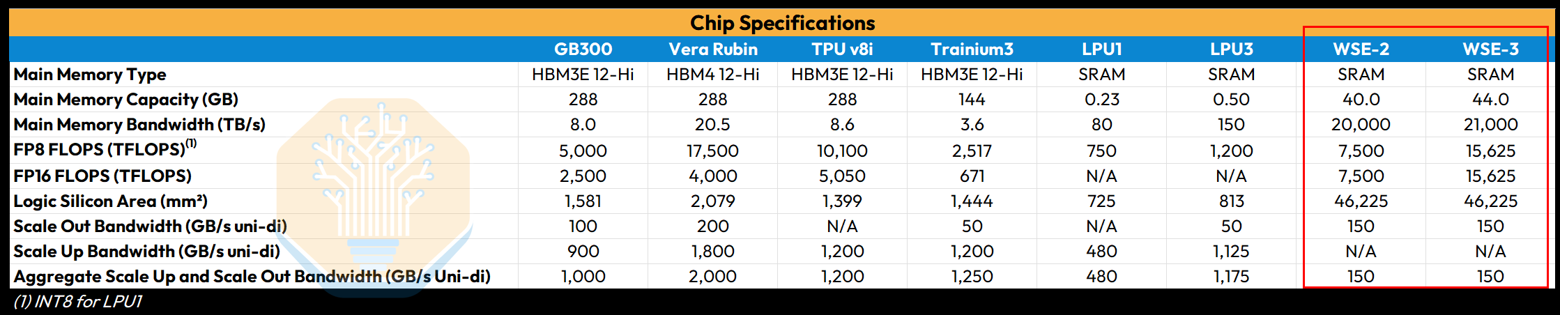
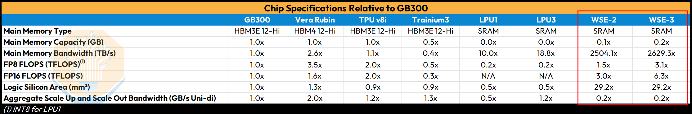
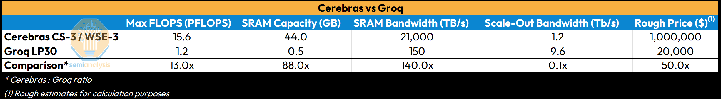
Cerebras is on its third-generation product, WSE-3, which is fabricated on TSMC’s N5 node. One WSE-3 has 44GB of SRAM across a wafer or “single chip.” This is a lot of SRAM. A typical large processor has on-chip SRAM in the 100s of megabytes. Even the Groq SRAM machine is only 500MB for each LPU3. SRAM is very fast, so it can deliver 21PB/s of bandwidth, thousands of times more than what HBM offers. Again, this is significantly more than the very high bandwidth Groq LPU due to the WSE having several more banks of SRAM and with the bandwidth of individual banks aggregated together.
While Cerebras markets a lot of FLOPs for the WSE-3: 125 PFLOPs of FP16 compute, this is a sparse number, not a dense number. This is taking a page out of the Jensen Math playbook but taking it further. Unlike Nvidia, Cerebras doesn’t actually state dense FLOPs in public WSE marketing materials. However, Cerebras assumes 8:1 unstructured sparsity in its sparse number, so dense FLOPS is actually 1/8th or 15.6 PFLOPS of FP16 compute throughput. We call this “Feldman’s Formula.” For the CS-2/WSE-2 a 10:1 ratio was assumed – as we see below, the sparse and dense spec is an order of magnitude different. While WSE-3 still wins on absolute compute throughput relative to other chips, compute per silicon area is not that impressive, especially today. This is likely down to each core being much smaller than a GPU’s functional array size, which is necessary for the purposes of yield harvesting, which we describe below.
The last part is off-wafer networking, which stands as the weakest part of the WSE. In total there is only 150GB/s of bandwidth, a fraction of GPU/XPU competitors who place huge importance on network to scale capability. We will talk more about the implications of low I/O as well as the structural difficulty in adding more I/O.
In summary, the WSE is a very big chip with a lot of SRAM, a decent amount of compute but not that much relative to silicon area, and almost zero network. We will now talk about the implications of this.
SRAM Machines
Where the WSE is clearly very strong is SRAM capacity. Like Groq’s LPU, the WSE is in the class of accelerator we call “SRAM machines,” where more silicon area is dedicated to super-fast SRAM, which is used as the primary memory where model weights and KV Cache are stored. In contrast, mainstream GPUs and ASICs such as TPU and Trainium use HBM to store model weights and KV Cache. They still have SRAM, just less of it. In general, trading HBM for SRAM means much higher bandwidth, lower latency and faster token output, but at the cost of capacity and therefore total throughput per {chip, watt, $}. SRAM is also just a lot more expensive per bit. Here is a chart from our recent article on NVIDIA + Groq’s use of SRAM comparing the technologies:
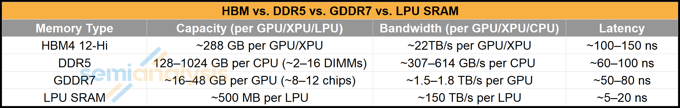
Even though the WSE-3’s 44GB of SRAM is a huge amount of SRAM relative to any other chip, it is not much more capacity than the 36GB provided by a single stack of HBM3E 12-Hi. With the norm trending towards 8 stacks per accelerator, this is 288GB for a single GPU or TPU package (e.g. the current generation Blackwell Ultra), which is 6.5x more than the SRAM capacity of a WSE.
Some readers may have noticed that DRAM has been in demand, and a lot of it is because AI system designers are trying to pack in as much capacity as they can. More memory in a system allows model providers to:
1. fit a larger model (more parameters)
2. serve more concurrent requests, i.e. more users (more KV Cache)
3. support larger context windows, i.e. larger sequence lengths per request (more KV Cache)
Inference providers make a business out of using all the above, which is why memory capacity per GPU is increasing. Not only that, but usable memory is not limited to a single package, since a workload can be sharded over multiple chips and aggregate memory can be pooled together within a scale up fabric. That’s why networking is such a key competitive battleground for all the AI hardware companies. That is, all of them except for Cerebras who have accepted the trade-off of little network and are working around it. So, with on-wafer memory capacity limited, the escape hatch of networking more wafers together is also much narrower for Cerebras. The lack of network bandwidth, while not fatal, is certainly a handicap in the WSE-3 design preventing Cerebras from launching their business to the stratosphere.
With that said, Cerebras is now on the path to being a healthy and rapidly growing business, with its OAI deal being a game-changer: until 2028 Cerebras will need to ship an order of magnitude more servers than they have since inception. The demand surge is already visible in TSMC’s wafer loadings, which step up materially each quarter through the year to meet OpenAI’s deployment requirements. We expect Cerebras revenue to inflect sharply in the coming years, with OpenAI as the primary growth driver.
Cerebras’s Technology
To reach this point, Cerebras has had to solve many technical problems from silicon to system to software. To their credit, there is a lot of proprietary hardware technology here, especially when compared to the innovations (or lack of) that a lot of other accelerator startups bring to the table. The wafer is a bold bet and not easy for incumbents and competitors to replicate.
Some of Cerebras’s proprietary technologies include:
1. Cross-die wiring and routing. Cerebras uses the scribe lines as wiring for the on-wafer data fabric that connects all the dies together. In a typical wafer, these are keep out zones where the wafer is diced to singulate individual dies.
2. Redundancy and failure routing. For the purpose of having an acceptable level of yield, the ability to route through defective cores is critical. Defects are inevitable especially for near reticle-sized units. Typically, dense processors that are near reticle sized have sort yields of well below 50%. For the sake of redundancy, there are a total of 970,000 cores on the WSE, of which 900,000 are enabled. Each core is deliberately made much smaller for the sake of better yield harvesting. However, this is not simple and there is a significant additional cost required. One of the interesting things done is that each batch of wafers will have a custom mask set for the upper metal layers. This is for the purposes of having different wiring for each batch to route around all the defective tiles. The cost of additional masks is a material increase in cost on top of the nominal TSMC wafer cost. Why is this for every batch of wafers? This comes down to intra-batch process variation being lower than across different batches. Read here to learn more about semiconductor manufacturing process variation. The net result of this is that wafer-level yield ends up being high. Nearly 100% of the TSMC wafer output is good enough to be assembled into a production server.
3. Power delivery and cooling. One of the major challenges that Cerebras has solved is getting over 20KW of power into one wafer, and it will be even more next gen. This much power necessitated the need for a custom power delivery solution from Vicor. This power will of course be turned into heat that needs to be removed, which requires specialized cooling. The power delivery and cooling sub-assembly in each CS server is called the “engine block.” This is another key component which, like the WSE silicon itself, is uniquely architected for Cerebras.
Despite these commendable technical achievements, the WSE architecture runs into a few technical limits that constrain their technical roadmap and ability to serve tokens.
Thermal Design and Cooling
Cooling 25 kW in a single 46,225 mm² wafer is the central thermal problem in CS-3 design, which translates into roughly 50 W/cm² averaged across the die, before accounting for hotspots. Air cooling was rejected because a 3D vapor chamber heat spreader (like we see in HGX H100 servers), scaled to span the 21.5 cm die, exceeds its wick’s capillary limit and dries out before working fluid can return to the evaporator. The CS-3 uses a custom liquid-cooled stack that presents architecture, flow rates, and rack-level plumbing different from Nvidia’s more recognizable direct-to-chip single-phase deployments.
The thermal solution is 100% custom and co-designed with the wafer. The silicon and the PCB underneath it expands at different rates as they heat up, and across a 21.5x21.5cm wafer that mismatch is large enough to crack a conventional package. The cold plate, the connector that bridges wafer to PCB, and the assembly tooling all had to be built from scratch. Cerebras calls its system the “engine block”, a four-layer sandwich including the cold plate, wafer, compliant connector, PCB, with the cooling manifold mated to the back of the cold plate. We will go over the system architecture in more detail in the next section.

Heat rejection runs through the cold plate. Coolant flows through micro-fin channels machined into the back of a copper plate. The wafer-facing side of the plate is polished and held against the silicon under preload, letting the two-slide relative to each other as they expand at different rates while maintaining contact to spread heat.
We find another architectural challenge at the rack-to-CDU interface. The OCP/Nvidia reference design for GB200 NVL72 sizes facility-side flow at ~1.5 LPM/kW. That constant is the one the majority of today’s CDU fleet is sized against. The WSE-3 runs at around ~100 LPM at 25kW, roughly 4 LPM/kW, or ~3x the NVL72 reference. That delta forces operators to use larger pumps, larger pipes, oversized CDUs, and quick-disconnects rated for higher flow. We believe that CS-4 should bring rack-level flow back toward 1.5–1.7 LPM/kW, which, if delivered, would converge Cerebras onto standardized infrastructure.
One of Cerebras’s main cooling partners is LiquidStack, which Trane Technologies acquired in March 2026. LiquidStack and Cerebras initially started working on two-phase solutions, and they have jointly developed L2L single-phase CDUs sized to the CS-3’s flow and pressure envelope.
Inlet temperature is a final axis where Cerebras diverges from other chips. Cerebras’s Oklahoma facility runs a 6,000-ton chiller plant producing 5°C (42°F) chilled water, which is then warmed across a heat exchanger to ~21°C (~70°F) before reaching the engine block. NVL72, by contrast, is specified up to 45°C (113°F) inlet temperature, which lets operators run free cooling for larger portions of the year. The CS-3’s wafer-level heat flux requires the colder envelope, and the cost is a chiller-heavy facility.

The CS-3 Architecture and BOM
Let’s take a step back from liquid cooling and zoom out to the Cerebras CS-3 system.
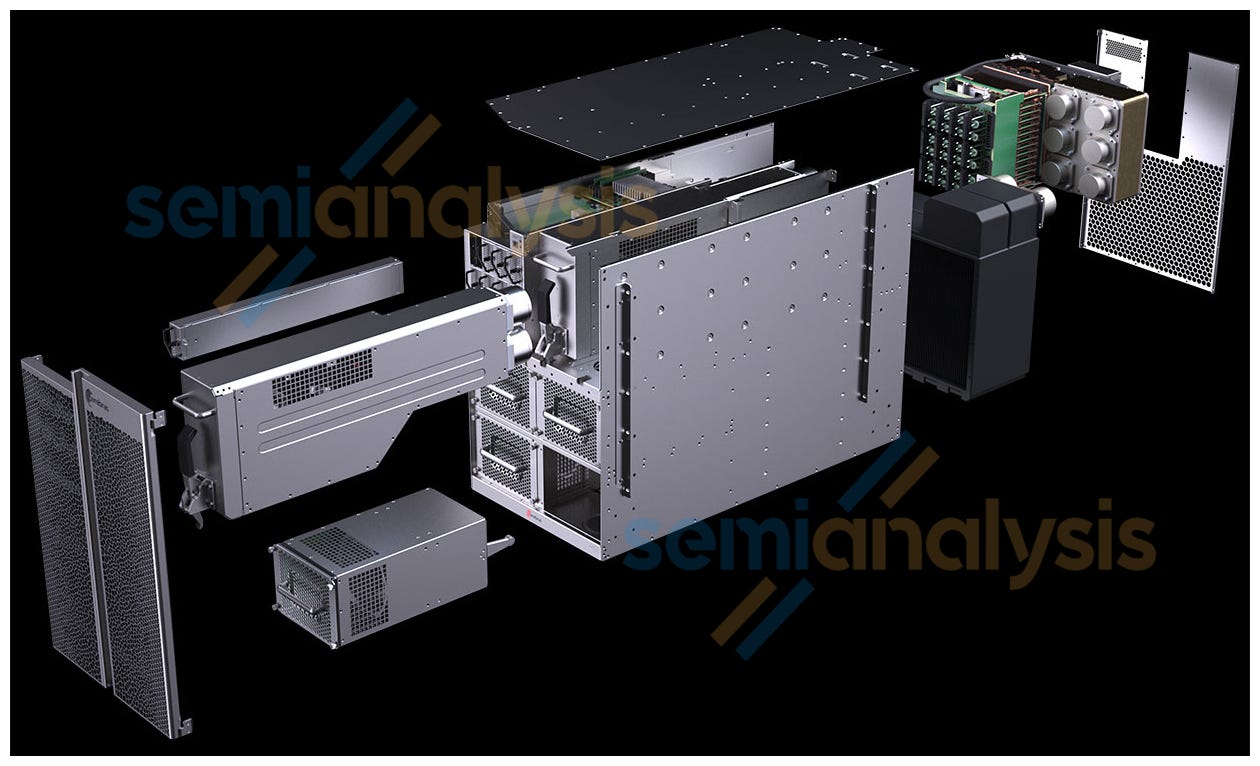
Each CS-3 includes the following: one WSE-3 engine block, peripheral compute and I/O modules, two mechanical pumps, 12 3.3kW power supply units, and a liquid-to-air or liquid-to-liquid cooling system.
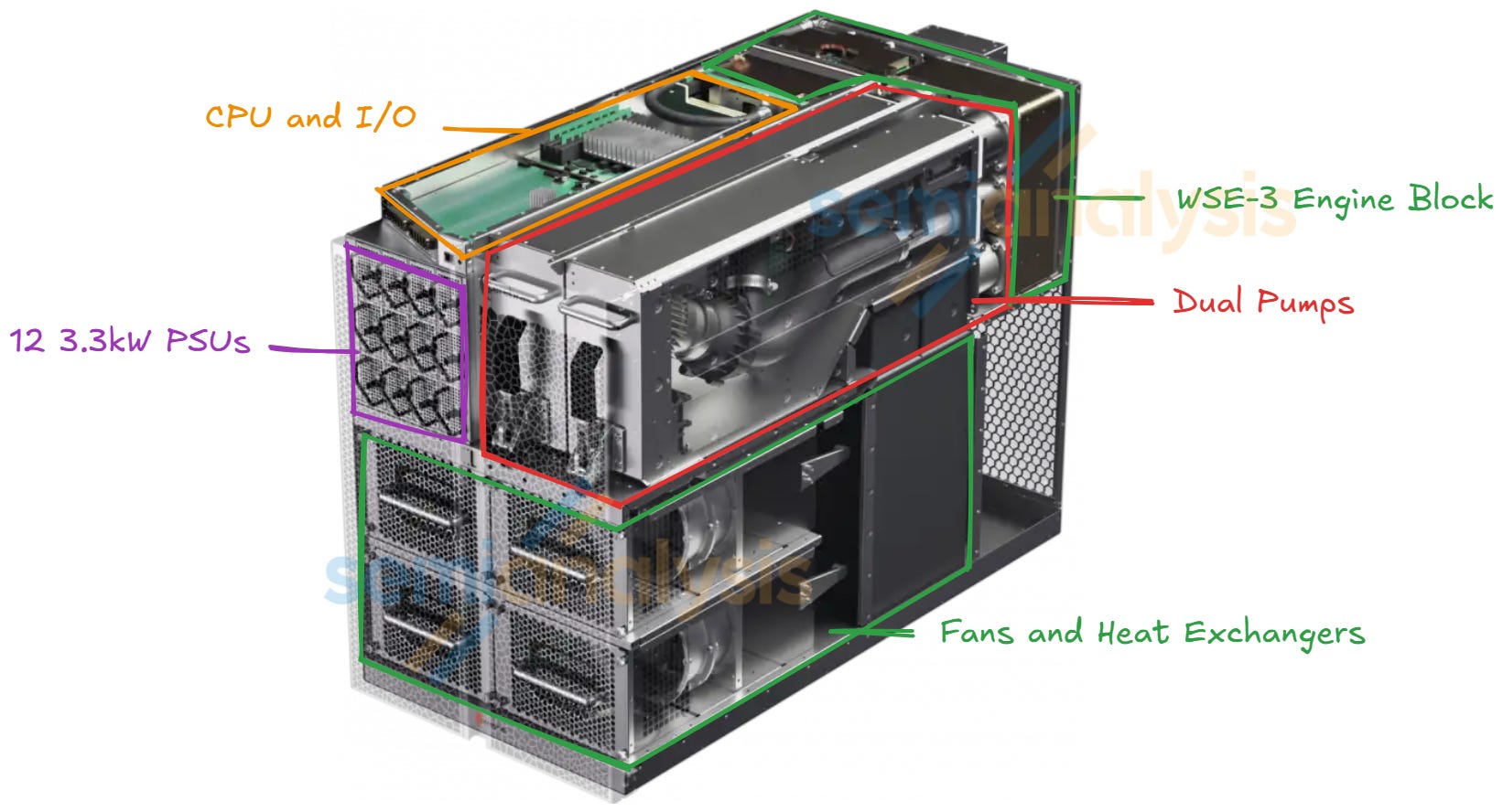
Zooming into the WSE-3 engine block, the WSE-3 engine takes in 25kW of power alone. Power delivery and cooling of the WSE-3 wafer is extremely customized and innovated. The power is fed into the WSE-3 engine block via the blind mated power connectors from the 12 3.3kW power supply units. The PSU delivers power at 50V to 12 PDB boards that stack on top of each other horizontally. Each PDB board matches to a row of 7 Vicor power bricks, which matches to a row of 7 blocks on the WSE-3 wafer. With 12 PDB boards, that is 84 power bricks and 84 blocks on the WSE-3 wafer. Then, 12V power will be delivered to Vicor’s power delivery module which is on the PCB with the WSE-3 wafer on the other side, and the Vicor brick will convert the power to 1V before sending it to the wafer. The WSE-3 is socketed onto the customized PCB via an elastomer socket.
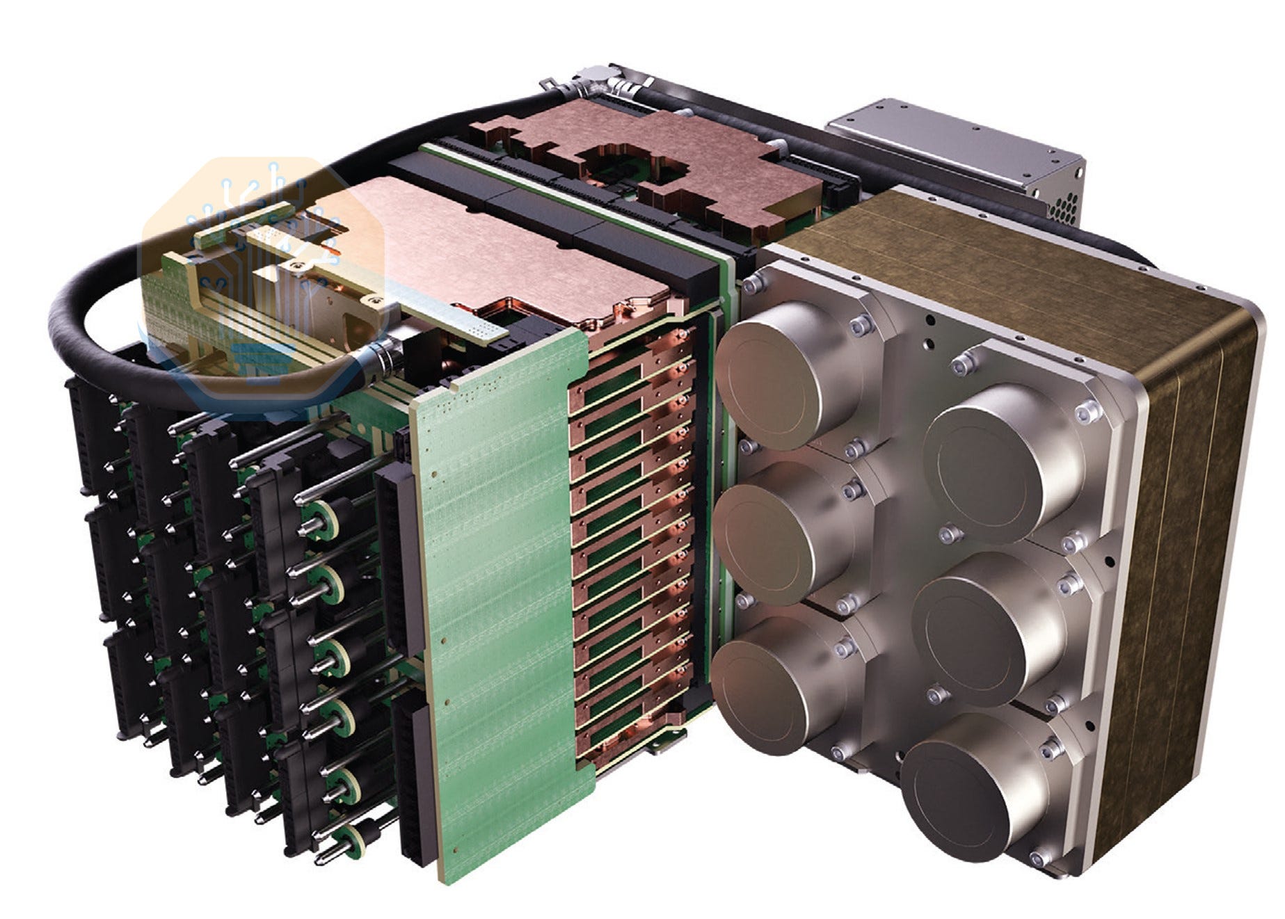
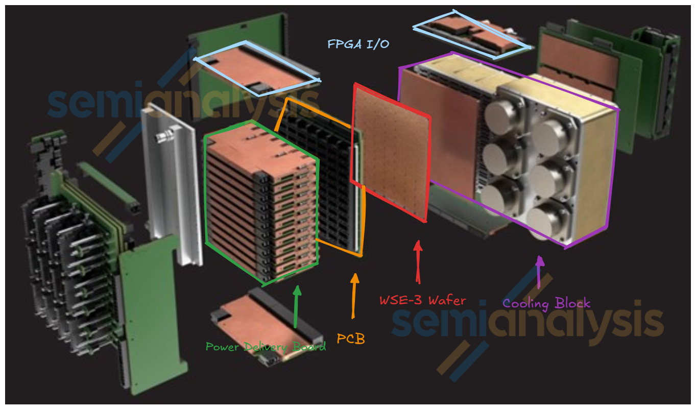
At the top of the WSE-3 engine block sits the I/O FPGA module connected to the WSE-3 PCB via board-to-board connectors. These FPGAs essentially serve as NICs that take in the Cerebras proprietary I/O off the wafer and converts it to Ethernet for scale out as well as PCIe. Customized cold plates are attached to the WSE-3 engine, the Vicor power delivery module, the CPUs, and the I/O FPGAs. The cooling loops connect to the manifold on the right side of the WSE-3 engine block. The manifolds have 6 couplings, in which 4 goes to the pump and 2 goes to the liquid-to-air or liquid-to-liquid heat removal system.
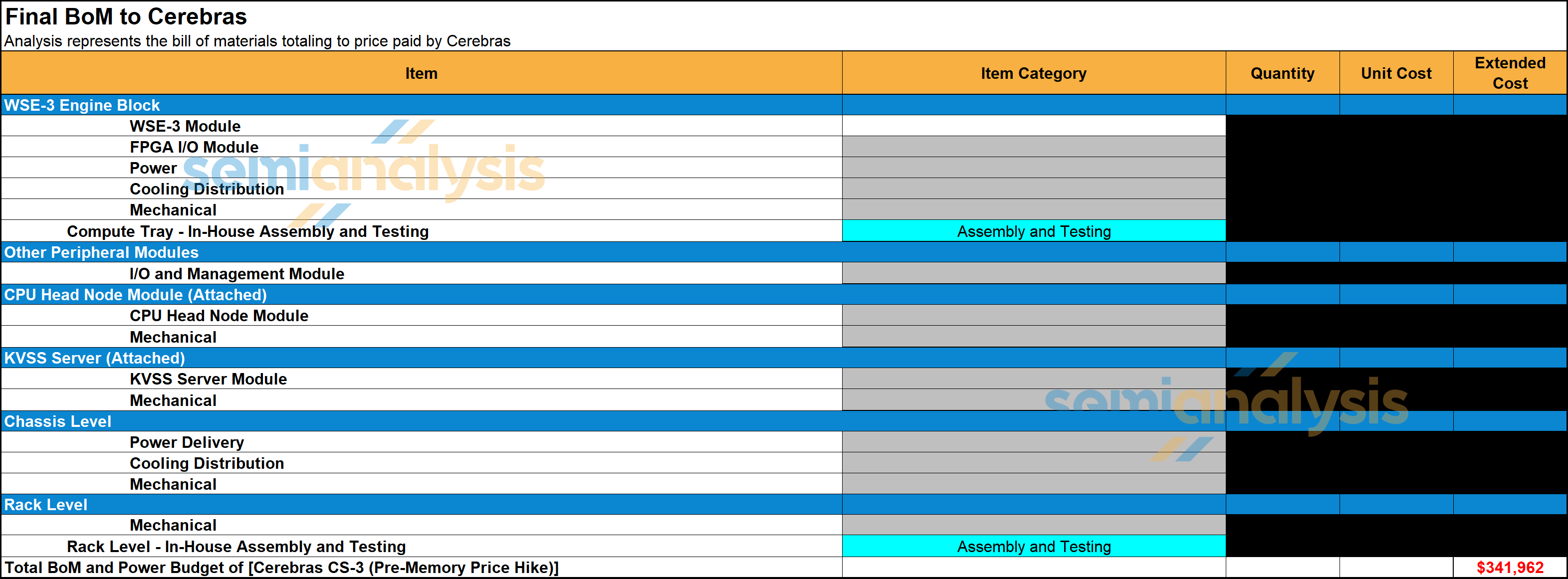
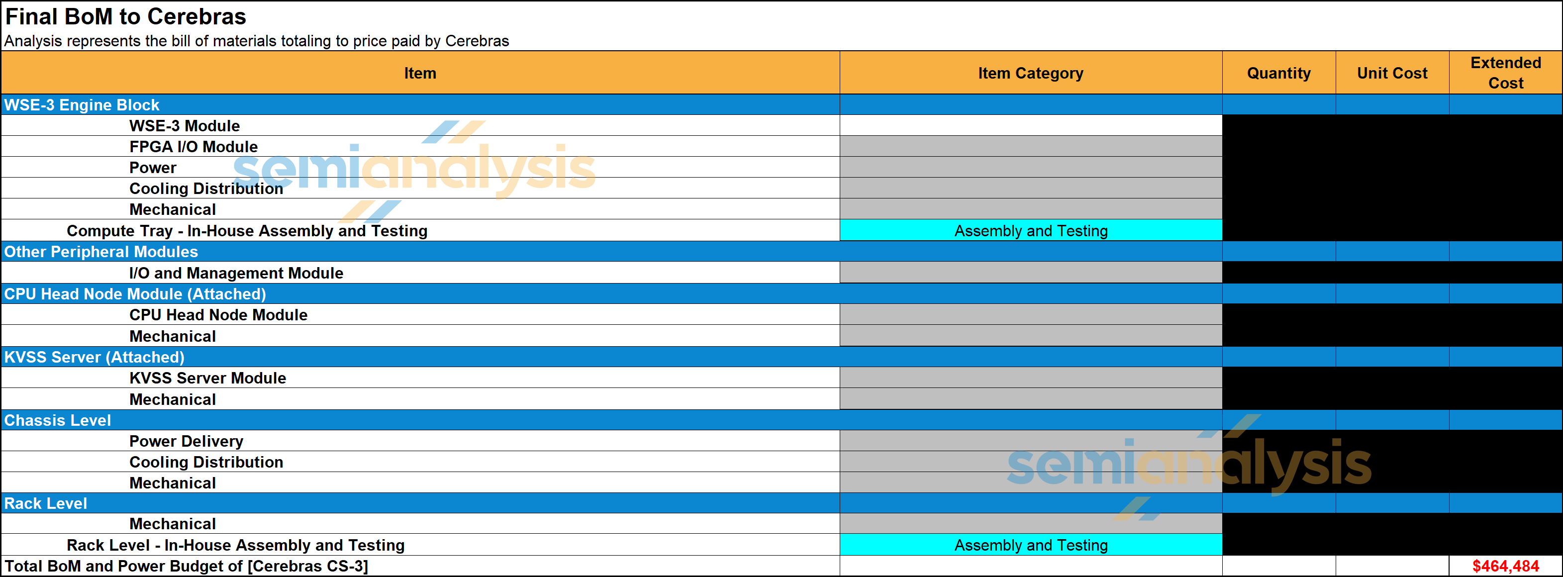
In addition, each CS server has a separate ‘KVSS’ node. This is a dual socket AMD CPU node with 6TB of DDR5 RDIMM which is used for KVCache offload. We estimated the BoM cost of the CS-3 system and the KVSS CPU node to be $350k USD per rack before the memory price hike that started in Q4 last year. Accounting for the latest memory price hike, we have raised the estimate of the BoM of the CS-3 system and the KVSS CPU node to $450k USD per rack.
This is very high especially relative to silicon content. While nominally the accelerator silicon, usually the most expensive part of the server, is one TSMC N5 wafer that costs around $20k, there are a lot of additional costs. The requirement for masking for each wafer substantially adds to the costs. The other major BOM item is the power delivery modules from Vicor. This is a custom VRM that needs to deliver 25kW to a wafer and uses VPD. The bespoke nature of this also means a high cost, and we believe VICR’s content in each WSE is not too far from TSMC’s content. The same goes for the customized cooling solution. Assembly and packaging are also performed in-house by Cerebras rather than at a contract manufacturer. There are also some peripheral components like 12x 100GbE Xilinx FPGAs that effectively act as NICs converting the Cerebras’s own I/O into Ethernet for external comms.
Where the Wafer Wins
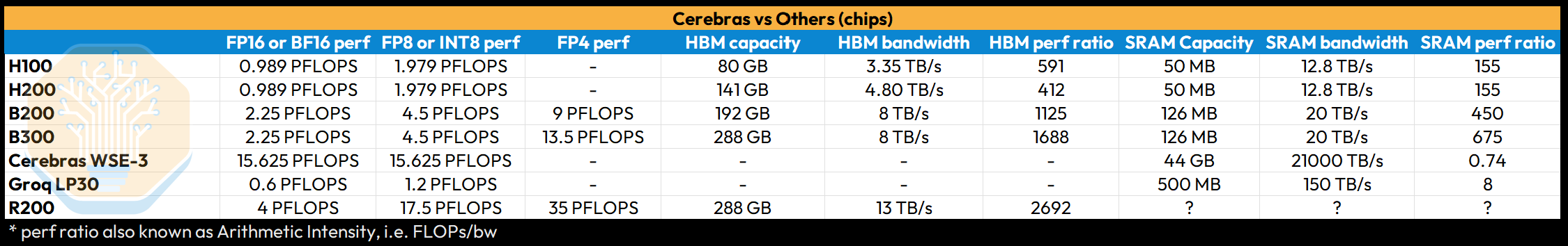
To understand the extremely high memory bandwidth of Cerebras in context, one must put on the hat of a performance engineer working on LLM inference. To performance engineers, a chip is a tool. Whether you are using 10,000 LPUs, 72 GPUs, or 1 wafer to get the job done, what matters is the “arithmetic intensity” of the chip – how many FLOPs the chip can perform for every byte it transfers to/from memory (FLOPs/byte). Below is a table of chip specs to put the WSE-3 in context. Note that these are theoretical maximum numbers.
On a relative basis, the performance of AI applications depends on the performance of individual kernels (i.e. software that runs on the device, not the host CPU) on these chips. The canonical example of a kernel used in AI is GEMMs (general matrix multiplication). GEMMs can have different shapes, dictated by the shapes of the matrices being multiplied. Certain shapes running on specific hardware can be memory bound (i.e. performance is limited by the available bandwidth), or compute bound (i.e. performance is limited by the available FLOPs).
It is striking to see the FLOPs of a WSE-3 compared like-for-like with NVIDIA GPUs. In terms of dense FP16 or INT8 FLOPS (the actual FLOPs that developers using a Cerebras WSE use), an entire WSE-3 is only capable of 15.625 PFLOPS. Compared to NVIDIA GPUs running native FP4, B300 comes in at 13.5 PFLOPS (or 15 for GB300) and the Rubin GPU has 35 PFLOPS. Of course, the astute reader will note that FP4 FLOPs and FP16 FLOPs are not always comparable, but with most production inference today shifting to FP4, it’s the best real-world comparison. Astute readers should also note the impact of Cerebras product marketing. Cerebras marketing materials, as well as their S1, claim much higher PFLOPs per wafer than our table shows. Thanks to the “Feldman Formula”, they use a factor of 8x (claiming 8:1 unstructured sparsity) to get there. An even bigger sparsity factor than the hallmark 2:1 rule of Jensen Math!
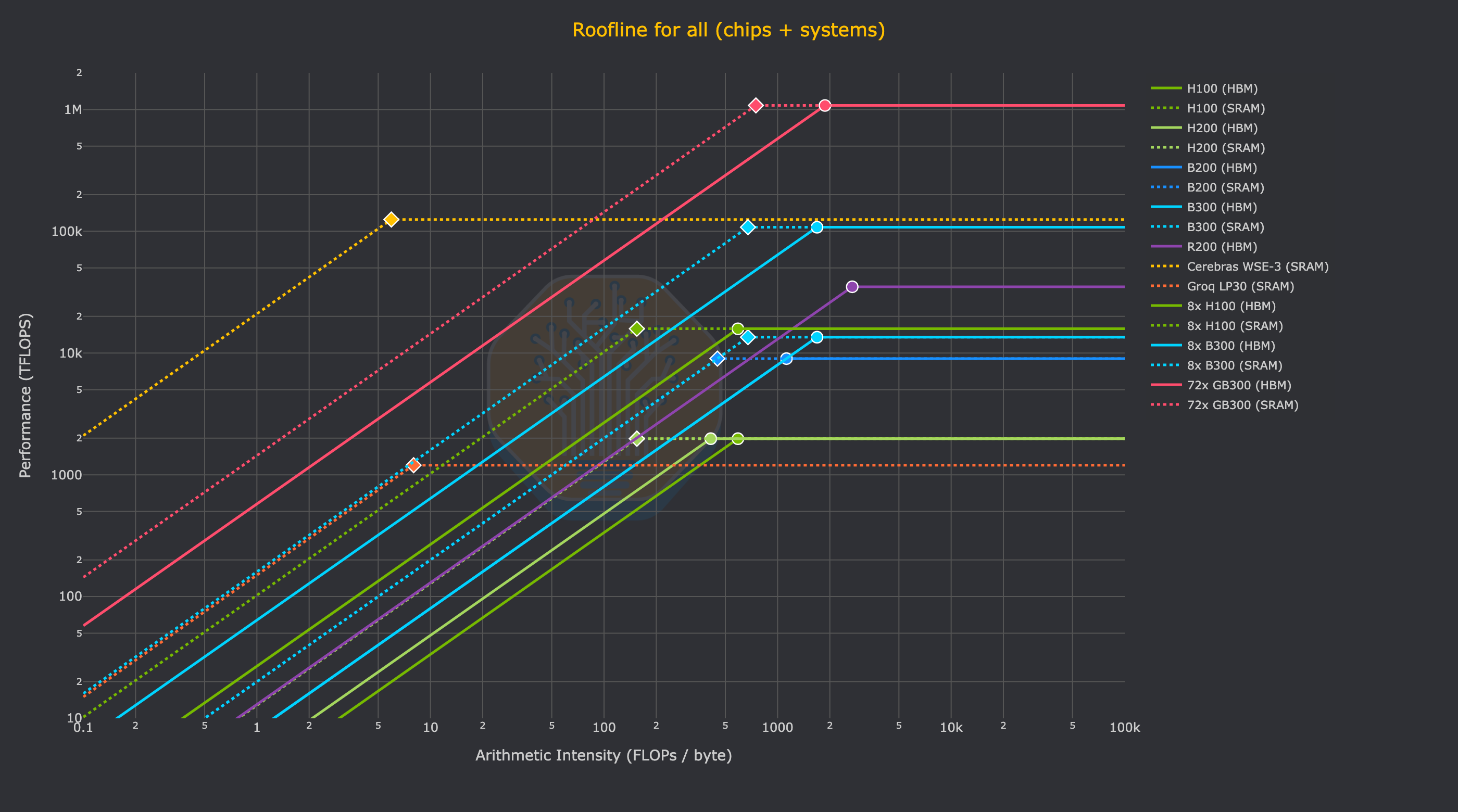
To compare Cerebras to alternatives, it is not useful to compare directly, chip-to-chip (or wafer-to-chip). We illustrate a more useful comparison below, with round numbers, to demonstrate where the wafer fits in.
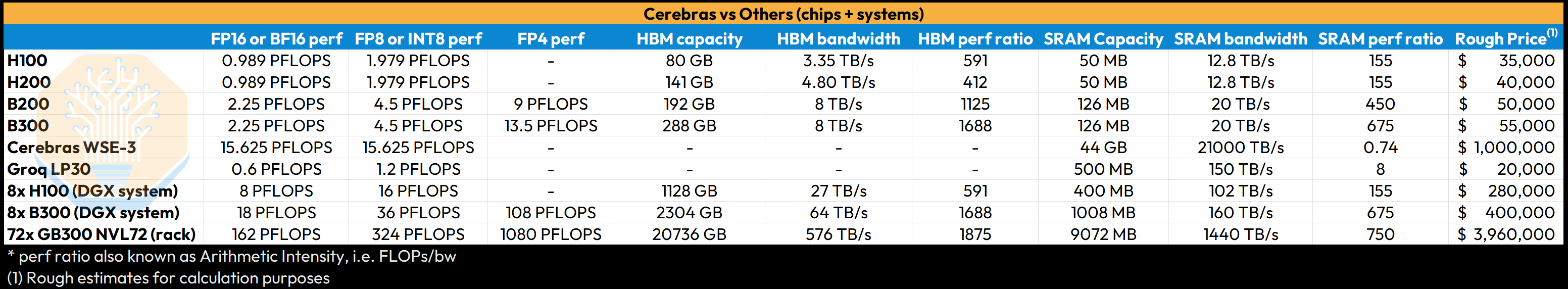
It is most instructive to compare a single wafer’s worth of cost and performance to around $1M worth of hardware on both HBM and SRAM. Namely: 2x NVIDIA HGX systems (16 GPUs), 4x NVL72 sleds (16 GPUs), or around 50x Groq LP30s. So, we will progressively add more rooflines to the plot in the following charts.
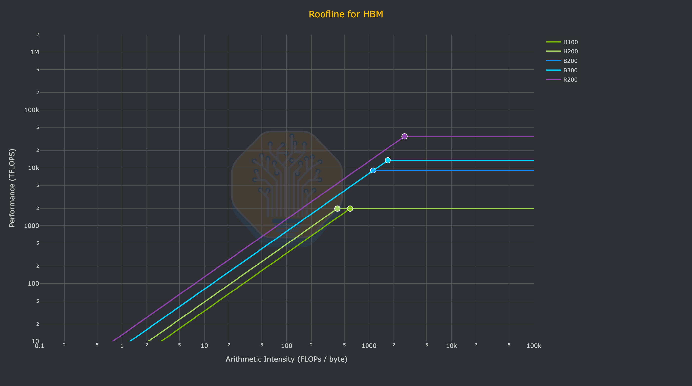
Here we see a single Nvidia Rubin GPU FLOP mogging an entire WSE-3:
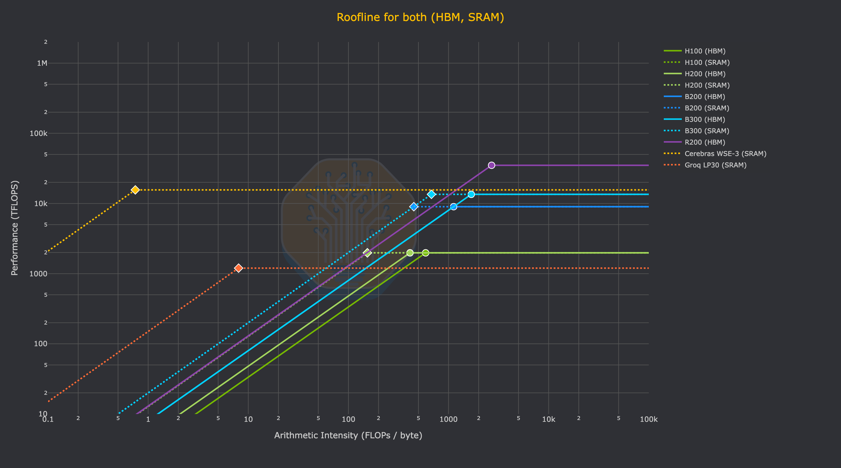
Finally, this chart demonstrates how this analysis can be extended to the system level (albeit in a naive way), comparing the roofline of a single Wafer’s SRAM to DGX systems and a GB300 NVL72 rack. One has to assume zero network overhead and add many racks of GB300 NVL72 just to be able to realize the same FLOPs as Cerebras on kernels with equivalent arithmetic intensity.
To finish with a complete understanding of which AI workloads are a good fit for Cerebras, we can just look at common GEMM shapes. GEMMs generally use “mnk” notation, meaning that the input matrices have size “m” and “n” respectively, with a contracting dimension of “k”.
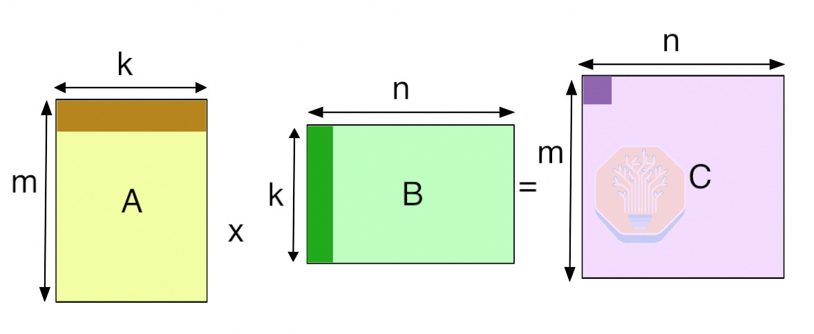
We can calculate the Arithmetic Intensity of a given GEMM using the following formula:
For reference, here are some example GEMM shapes used in LLM inference:
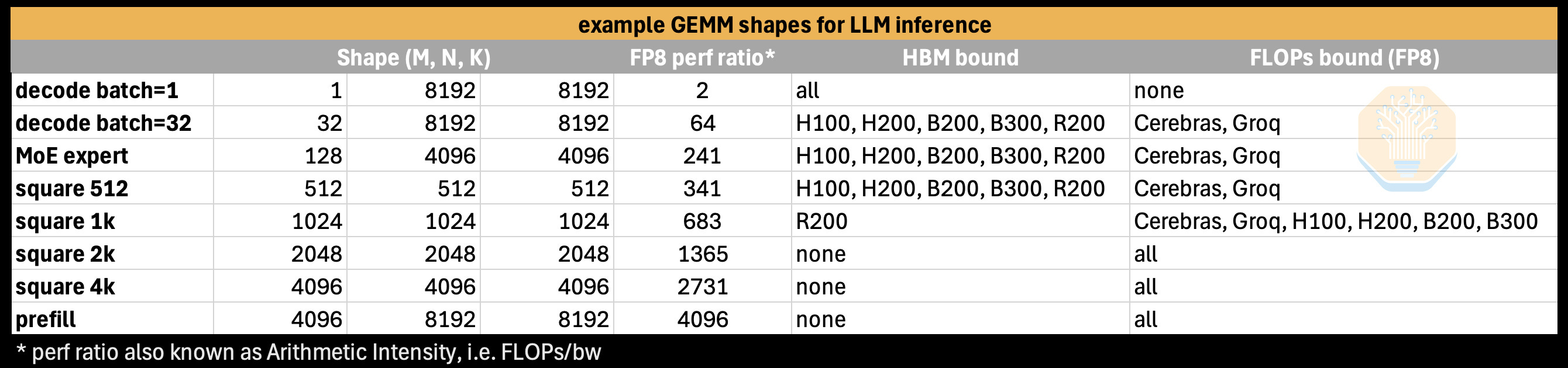
And finally, here is how those kernels would theoretically perform on different chips. Just trace from bottom to top on one of the vertical lines that represent the arithmetic intensity of a given kernel to see the (theoretical) performance that a given chip will be able to realize on that GEMM shape (measured in TFLOPs).
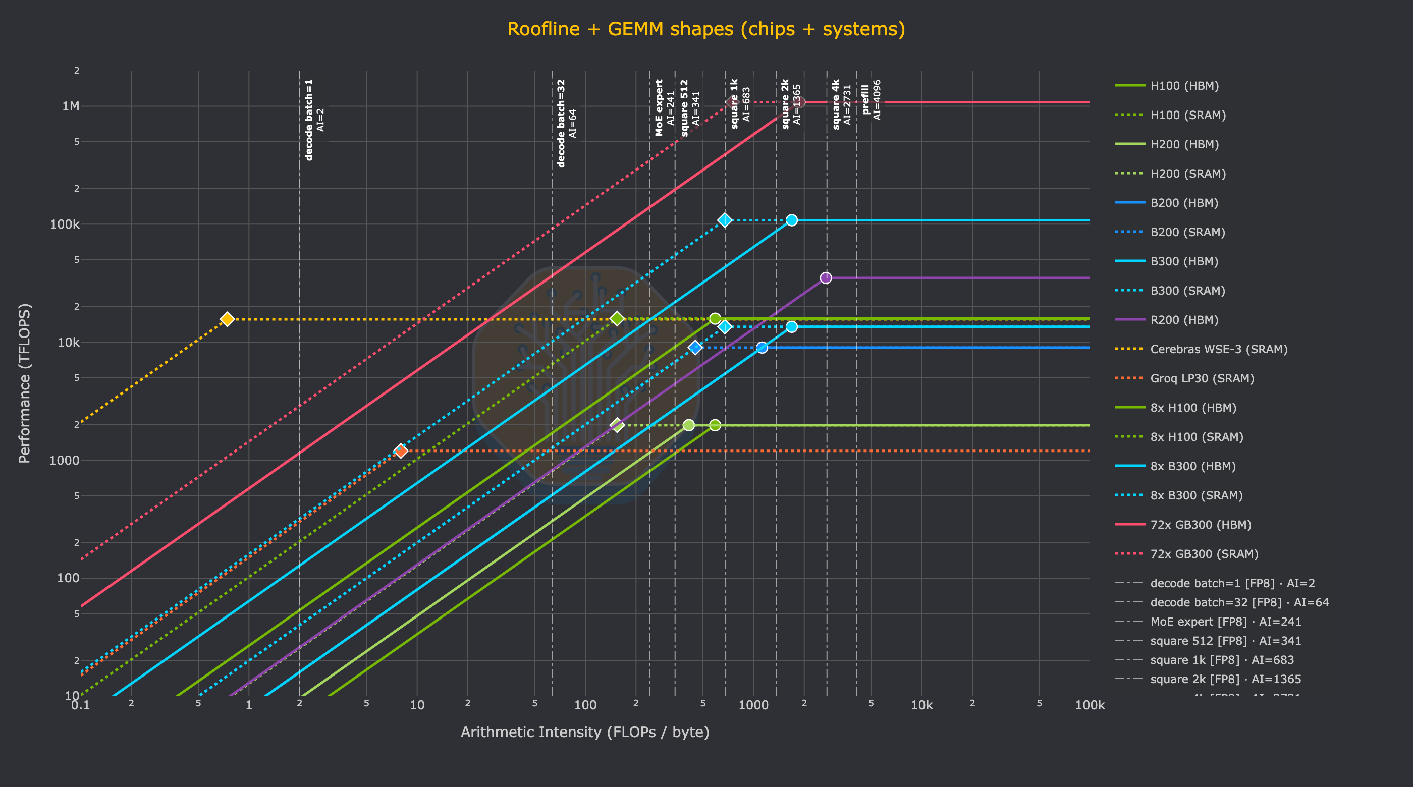
At a high level, it is clear that Cerebras has very unique performance characteristics, with an optimal arithmetic intensity of 0.74 on the WSE-3’s SRAM and FP16 or INT8 FLOPs. With HBM-based GPUs going the other direction over time, i.e. an arithmetic intensity increasing to over 1000, there is a clear difference between the GEMM shape (or more generally, which kernels) will make the most effective use of Cerebras hardware.
For the reader to get a sense of what the realized FLOPs looks like for a given decode kernel, just imagine a decode kernel with (m=batch=1) and arithmetic intensity of (AI=2). This is the leftmost vertical bar on the previous chart. As you trace your finger from bottom to top on that line you will cross many chips before you reach Cerebras: all NVIDIA GPUs and Groq LPUs will only be able to realize dozens or hundreds of TFLOPs in an absolute max, theoretical case. Meanwhile, the Cerebras wafer can (again, theoretically) realize its full 15.625 PFLOPs. This is the key point of the wafer. Absolutely massive amounts of memory bandwidth from the 44GB of SRAM on the wafer mean that decode kernels can realize equally massive amounts of performance.
Going back to our job as a performance engineer, this means that decode kernels with low arithmetic intensity have a much higher theoretical limit in terms of the amount of FLOPs that can be realized. The SRAM bandwidth can keep up with the compute, while the HBM of a GPU running the same kernel leaves Blackwell SM100 FP4 Tensor Cores starving. And as a result, the types of models and workloads that will be designed to run on the Cerebras WSE-3 in the future, such as GPT-5.3-Codex-Spark (with an architecture that also goes by the name of gpt-oss-120b), will be developed with the performance characteristics of the wafer in mind.
A perfect example of hardware-software co-design.
The Wafer Taketh and the Wafer Giveth
The WSE has several clear weaknesses that we have mentioned. It has a lot of SRAM, but given SRAM is inherently not dense on a per-watt or per-dollar basis, HBM-based GPUs and XPUs offer far more memory capacity per watt or dollar. This HBM is currently used to serve larger models with longer context length, as well as more batching of users to drive throughput. Networking more wafers together to overcome the lack of memory per wafer is also constrained by the lack of off-wafer bandwidth. Absent a heroic technical achievement (hybrid bonded optical transceiver wafer anyone?), both these issues are an intentional part of the Cerebras architecture and make it hard for Cerebras to economically serve large models or even medium size models with long context lengths, that are representative of today’s agentic workloads.
To illustrate this point, we have made an interactive calculator available at tokenomics.info/cerebras. This is a taste of the kind of research that our Tokenomics subscribers get.
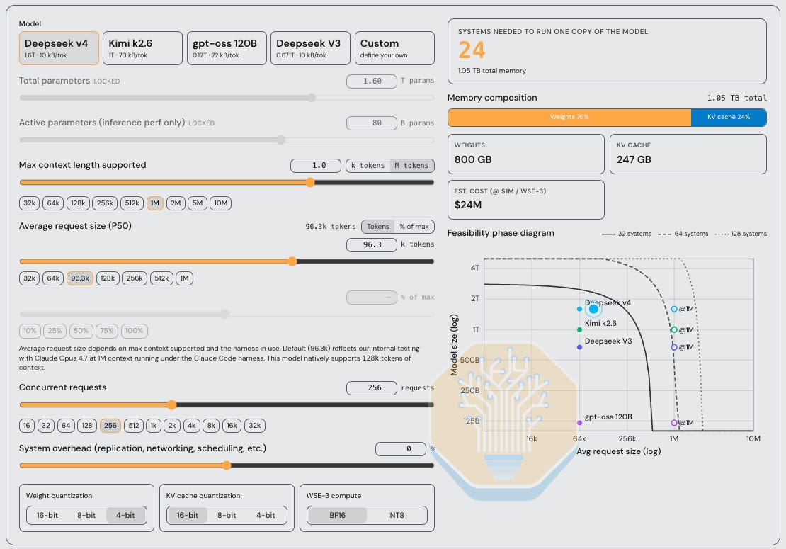
As shown above, when adjusting the average request size, number of concurrent requests supported, model size, and quantization for weights and KV Cache, the total number of WSEs required to run inference varies significantly. This, of course, leads to different performance characteristics on inference or decode, and $/Mtok cost conclusions.
A notable assumption in this calculator is our 96.3k average request size. While Cerebras chooses to build their inference product for their customers around an assumption of 64k avg request size, we believe this is an artifact of running models with limited context windows of 128k. In other words, confirmation bias in action.

To get an understanding of exactly what real-world traffic patterns are, we built a proxy that collects fully anonymous traces from popular agentic coding harnesses such as Claude Code, Codex, Cursor, and OpenCode. This is part of an ongoing effort to collect production agentic traces for offline replay on InferenceX.
A relatively large sample size of ~432k requests (about 80B tokens) leads us to believe that a typical P50 ISL is ~96.3k tokens, not 64k or fewer. We also deduce that the P90 or P95 requests can be exponentially more valuable than the initial requests and still critical to support. In total, almost 50% of our requests are over 128k, which is the maximum context window that Cerebras currently supports on public endpoints. Many sessions we see have an initial context length of over 100k tokens due to tool use context, system prompts, and things like skills and various other forms of primer context.
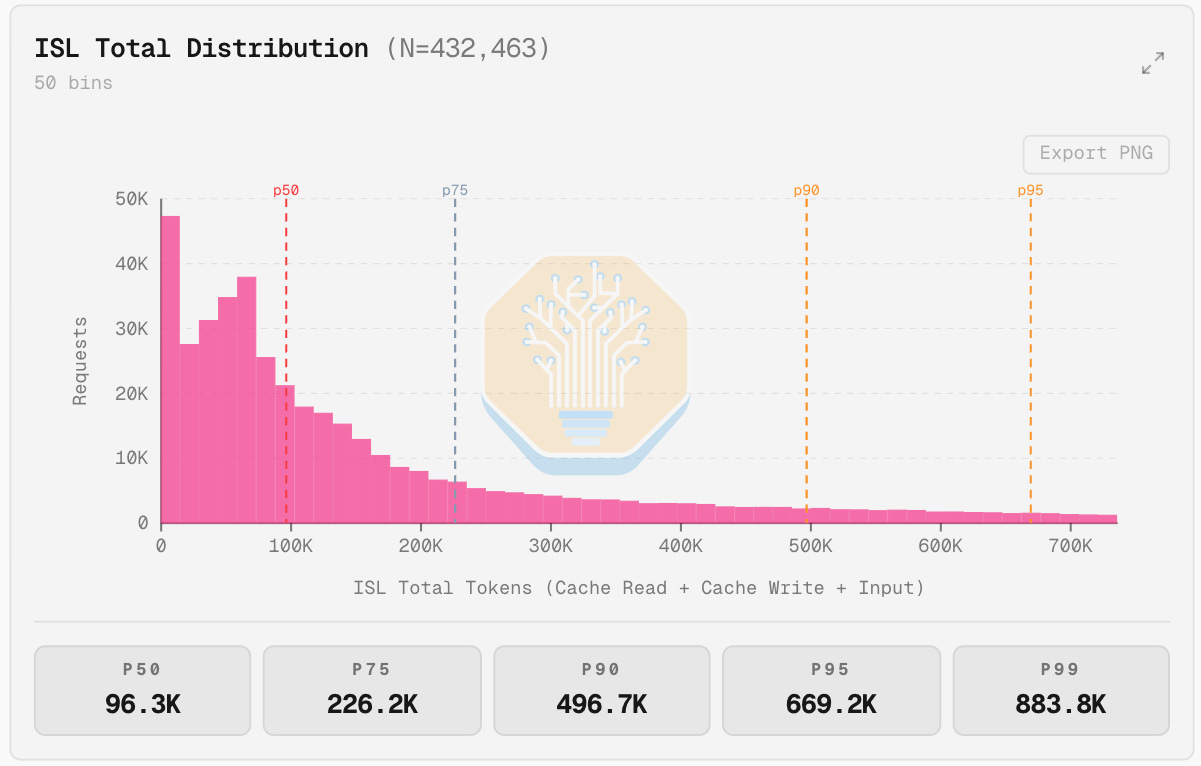
Moreover, the industry is trending towards larger context windows ad infinitum -- 128k context will certainly not be acceptable for long, especially with the prevalence of agentic workloads. The obvious conclusion of this analysis is that to run the latest open-source models with full context windows for real-world traffic patterns, Cerebras needs to deploy a lot of wafers.
Just for the DeepSeek v4 example above, with 24 CS-3 a CS-3 customer could get 5 GB300 racks. Each rack has 20TB of HBM which is easily able to absorb the model weights leaving over 19TB for KVCache. That is a lot of KVCache to serve more users and to support long sequence length, and there are 5 of these racks also. While we’ve shown the speed gap in favour of Cerebras, this is how the throughput gap is well in favour of HBM-based GPUs.
SRAM Scaling is Dead
Arguably, Cerebras is the company most exposed to the death of SRAM scaling, with Cerebras’s key draw being SRAM and 50% of wafer area dedicated to SRAM. It’s already showing up on their roadmap. WSE-1 on TSMC 16nm shipped with 18 GB of SRAM; WSE-2 on 7nm jumped to 40 GB, a decent 2.2x gen-on-gen. WSE-3 on 5nm advanced to just 44 GB. That’s a 10% increase across a full node transition, while logic transistor count grew ~50%.
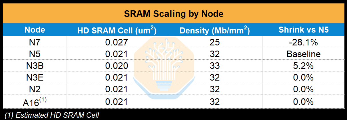
As we look to the future, this only gets worse. We can see that beyond 5nm (what the WSE-3 is currently fabbed on), SRAM scaling basically stops dead. The most common flavour of 3nm, N3E, has zero shrink relative to N5, and this continues to be the case for N2 and beyond. Now, the only way for Cerebras to increase SRAM capacity is by increasing wafer area dedicated to SRAM, sacrificing compute area. It’s a strict tradeoff when the chip is wafer scale. This is why the next generation CS-4 system will use the same N5 based WSE-3, but with higher power to sustain higher clock speeds and compute but stuck at the same SRAM capacity.
By comparison, this isn’t as critical for Groq as they are able to scale in the Z direction: using hybrid bonding to add additional SRAM tiles to vastly expand SRAM per package, which is on the roadmap for the Nvidia Groq LP40.
The logical path would be for Cerebras to do the same: wafer-on-wafer bond another wafer to expand SRAM and or compute per system. This is something that Cerebras is seriously exploring, having shown their concept of a DRAM wafer hybrid bonded onto the WSE to add more fast memory capacity. However, the timeline and technical feasibility of this is a concern for us given the litany of thermo-mechanical and bond-wave challenges. Yes, wafer-on-wafer bonding is an established process, but not where the whole wafer is stitched together as a whole chip. Cerebras has overcome these sorts of challenges in the past and will need to continue to innovate.
The Island Problem - bandwidth is geometry
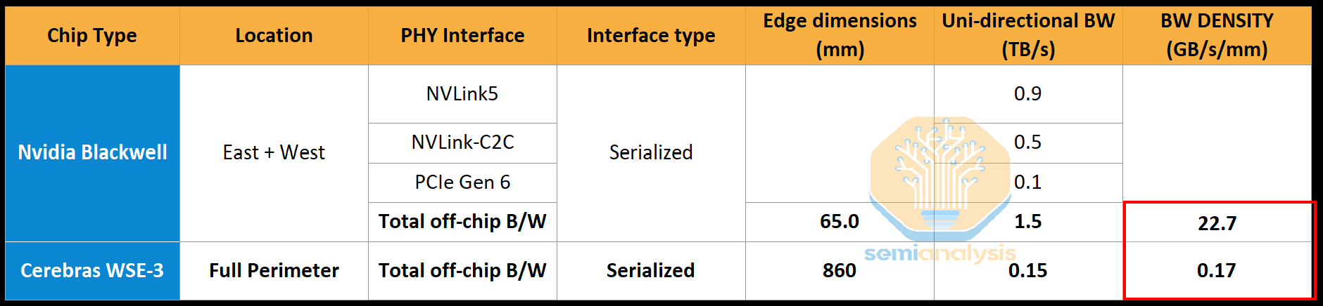
Despite the SRAM scaling issue, WSE still delivers an overwhelming amount of more compute and SRAM per single piece of silicon compared to other chips. Now comes the biggest tradeoff: the network. As mentioned earlier, each WSE has just 1.2 Tb/s (150GB/s) of off-package bandwidth. This is low compared to the average accelerator, and especially low relative to the amount of compute that the WSE has. No, this is not because the Cerebras architects have missed the importance of I/O for AI compute and overlooked adding more SerDes, this is just an inevitable tradeoff that comes with a wafer-scale chip.
By comparison, each Groq LP30 that NVIDIA will produce includes 96 lanes of 112G SerDes. That’s a 9.6 Tb/s pipe in and out of a much smaller chip. It is clearly well prepared for the PDD + AFD inference setup that Jensen debuted at GTC this year.
So why the bandwidth tradeoff? At the current 150 GB/s (1.2 Tb/s) of off-wafer bandwidth, that’s just 0.17 GB/s per mm of edge, so Nvidia’s off-chip I/O is 130x denser!
Cerebras’s lack of shoreline density comes down to the wafer scale architecture and reticle stepping problem. The WSE is patterned one reticle field at a time, tiling the same reticle pattern across the wafer in an 84-die array (12 columns × 7 rows on WSE-3). For the cross-scribe-line interconnect to work, every reticle exposure has to be identical, with the same logic, the same memory, the same routing, in the same positions. That’s what allows the on-wafer 2D mesh fabric to extend uniformly across die boundaries: every die’s east edge connects to its neighbor’s west edge with matching pin assignments.
This uniformity requirement is non-negotiable, and it has a punishing implication for IO. You cannot dedicate one reticle to PHYs while the other 83 reticles do compute. Every reticle has to be the same reticle. So, if you want more SerDes lanes on the wafer edge, you have to spend reticle area on SerDes in every reticle, not just the perimeter ones. Most of those PHYs will be in the middle of the wafer where they cannot reach the outside world, doing nothing. You pay a full silicon cost for IO that’s stranded inside the wafer.
An alternative, putting PHYs only in perimeter reticles, would require a non-uniform stepping pattern, which is unfeasible from a process point of view. It would require swapping out reticles on a partially patterned wafer which would introduce untenable process risk and complexity, especially given all these reticles need to be stitched together which breaks the cross-scribe-line interconnect that makes wafer-scale work in the first place (what we called the “scale-up network” earlier).
Even if Cerebras accepted stranded silicon and burned area on PHYs everywhere, they would hit a third constraint: on-wafer dataflow blocking. During inference, the on-chip 2D mesh fabric carries the activations, weights, and gradients between cores (again, why we called it the scale-up network). Every PHY block placed inside a reticle is a hole in the mesh, a region where compute and routing cannot exist. PHYs are large (high-speed SerDes are typically 1–3 mm² each at 5nm, including the analog circuitry that doesn’t scale with logic), and their analog circuitry is hostile to neighboring digital logic due to power and EMI concerns, demanding guard regions. Putting PHYs in the middle of the wafer means the 2D mesh fabric has to be routed around that area, increasing latency between reticles and reducing total bandwidth. Too much of this excess routing would defeat the purpose of going wafer-scale, since the whole point is fast and low-power dataflow across tiles.
In summary, the uniform tiling that makes wafer-scale possible (one reticle pattern, one mesh fabric) is what makes adding IO bandwidth hard. Cerebras must be looking for ways around this limitation.
A lot of the issues we just described come from the realities of moving data in the electrical realm, which are circumvented with optical I/O. The solution that Cerebras is working on (again proof that Cerebras recognizes the problem) is a photonic interconnect wafer hybrid bonded onto the WSE. As with the additional DRAM wafer to solve the memory constraint, the bandwidth constraint is also being addressed with another wafer.
Cerebras claims that for LLM inference they don’t need any more bandwidth and is only aggressively pursuing hybrid bonding wafer scale photonic I/O to help their HPC boomers. The HPC customers whom NVIDIA has effectively abandoned after reducing FP64 native hardware on their GPUs to basically nothing. This is great that Cerebras is aggressively reinvesting completely back into moonshot R&D instead of doing buybacks. Buybacks are not a good idea for companies that have lots of R&D things to reinvest into, for example, AMD did ~$221 million of buybacks last quarter yet internally multiple AMD internal teams continue to lack development interconnected GPU clusters.
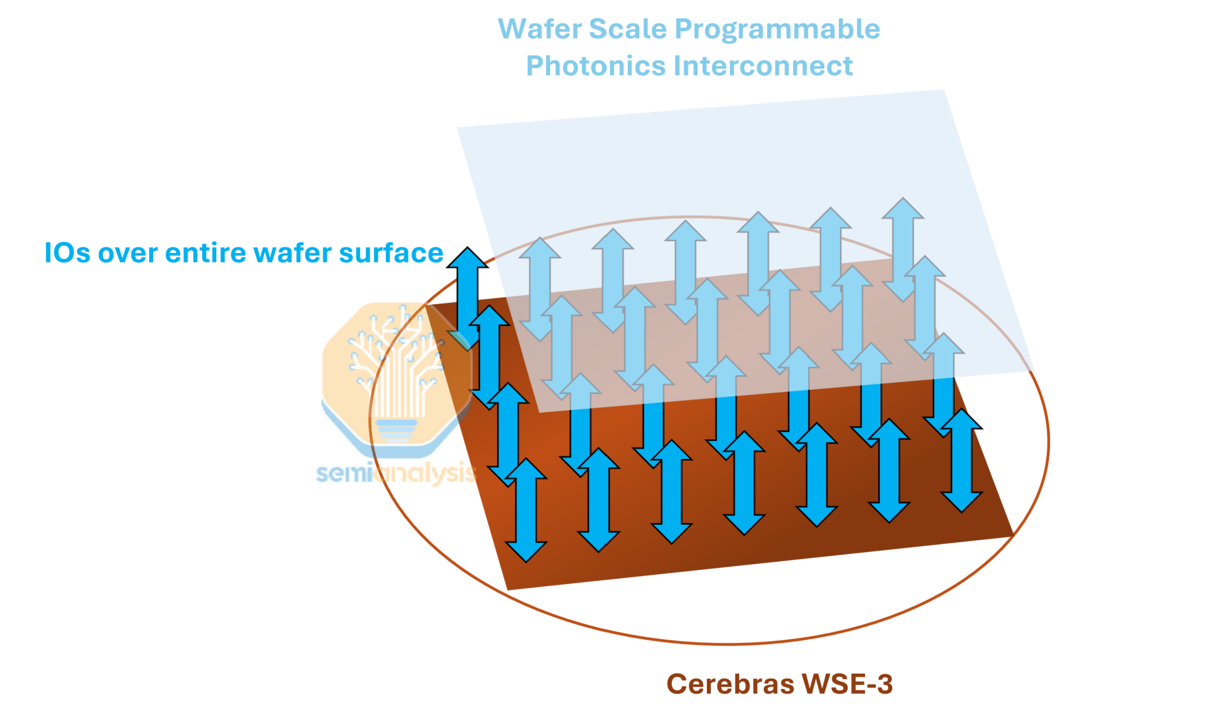
This allows data to move in/out of the wafer up through the z-axis, rather than having it go through the edges. The photonics partner developing this photonic wafer is Ranovus. This reintroduces the issues of WoW hybrid bonding for wafer scale silicon. Optical components are thermally sensitive (cannot be too hot or too cool) and it will be sandwiched directly against a wafer that runs hot. Lastly, there is the practical difficulty of fibers needing to be perfectly coupled off to the wafer. This is still being figured out at the optical engine level for conventional CPO, let alone for something wafer scale.
With all this in mind, let’s look at how the architecture shapes inference workloads
Pipeline Parellelism is Forced
One of the key concerns that we have already highlighted with using Cerebras in any inference deployment is just how big models have gotten. Both in terms of total parameter count (e.g. DeepSeek V4 is 1.6T total parameters), and in terms of KV Cache (256k context is the norm, with DeepSeek V4 debuting 1M context).
The combination of limited single wafer SRAM capacity of 44GB in the WSE-3 and low IO bandwidth results in challenges effectively serving models of these sizes.
Each CS-3 has just 12x100GbE of IO bandwidth -- roughly 150 GB/s for the entire wafer. This is one sixth of the scale-up bandwidth for Blackwell with NVLink5 at 900 GB/s per GPU, and an order of magnitude below the bandwidth of HBM.
This bandwidth constraint is what makes it difficult for Cerebras to serve larger parameter models. Any large tensors to be used must be resident on the wafer; streaming on/off the wafer is impossible with such a small amount of IO. Similarly, any sharding strategy that requires high-bandwidth collectives at each layer is categorically ruled out.
The only real option is pipeline parallelism, which slices the model layer-wise across wafers and only transfers activations between stages, relying on the fact that activations are small relative to weights. This reduces network requirements and keeps the capacity-demanding components (the weights, and to some extent the KV cache) stationary instead of moving on or off the wafer. For instance, Cerebras shards Llama3 70B across 4x WSE-3, transferring only the activations between each wafer and staying well within the available 1.2Tbps IO.
As you increase the number of wafers used to host the model, there are several factors to wrestle with to increase scale. First, the pipeline bubble: to keep N pipeline stages busy, you need at least N in-flight microbatches. A 4-stage config needs ~4 microbatches in flight; a 16-stage config needs ~16. Second, each in-flight microbatch carries its own KV cache, and on Cerebras that KV cache must live in the same 44GB of on-wafer SRAM that’s already mostly consumed by weights. Even if there is enough capacity in the SRAM with the heavily compressed KVs of recent models such as DeepSeek V4, the time to transfer the KV cache on or off the wafer is still quite large. Additionally, scaling the model size scales the number of wafers needed to hold the weights and therefore increases the number of times the latency of wafer->wafer activation transfer adds to the decode time.
In summary, the way the wafer is being used in production today basically goes against the entire ethos of the wafer. The whole point of the wafer is to run really fast at small batch sizes!
Running the Numbers
Let’s take a look at some napkin math with a few open-source model architectures to better understand how different models map to Cerebras’s SRAM footprint. Below are some rough ballpark numbers showing the footprint of several models.
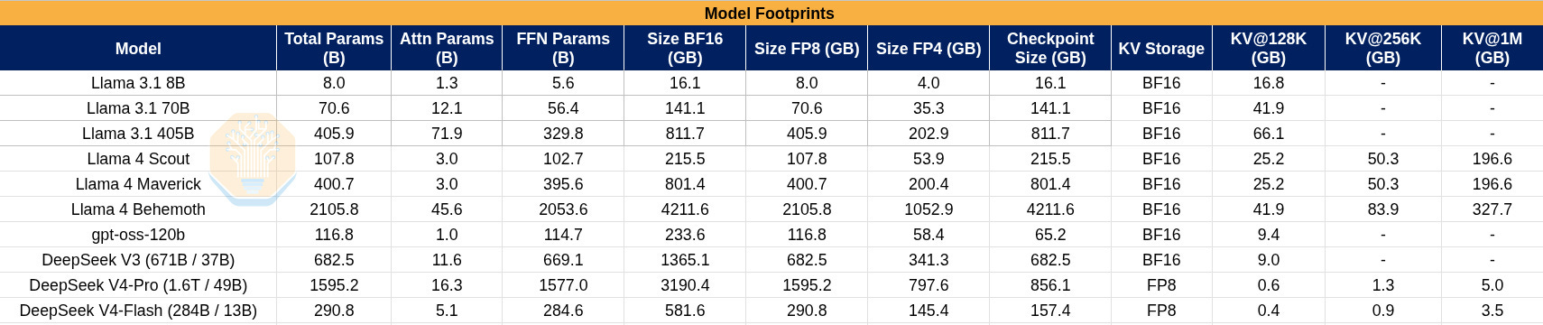
And now some rough numbers considering the WSE-3 specs. We make some assumptions here, including that the transfers will use the full 12x100Gbps.
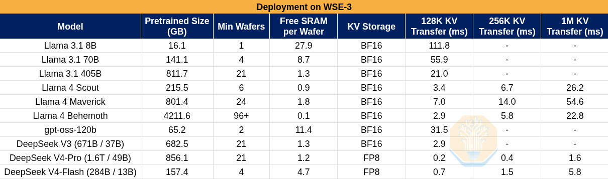
Here we define the minimum number of wafers to store the model weights by sharding strictly along layer boundaries, but we don’t include the space to store KV caches. In practice, more wafers may be used to give more space for KV caches. Activation transfer times are not included because activations are so small that their transfer will be bound by the propagation time across the I/O path.
It is clear from the table that recent KV cache compression techniques such as those published by DeepSeek might significantly alleviate issues Cerebras has with long-context serving. However, the problem of slow I/O does not completely disappear. Firstly, KV transfer times on- and off-chip are still quite large at several milliseconds, both impacting TTFT and making it more difficult to achieve high utilization due to issues of batching, pipelining, and latency-hiding related to KV cache storage and transfer. Secondly, the fixed I/O latency of activation transfer must be paid in proportion to the number of wafers used to host a model instance. This is a fixed cost in the TPOT that scales linearly with the number of wafers used to host the model.
The key takeaway is that Cerebras, while fast, pays a large latency cost to move data on and off the wafer, and therefore their cost-to-performance ratio (or perf per Joule) will depend on how much of that latency they can hide or minimize. A clue about the difficulty of this in practice may be reflected in Model offerings on Cerebras Inference Cloud. The largest production model is GPT-OSS, which is only 120B total parameters. There are larger preview models, but even those top out at 355B (GLM 4.7). For reference, Sonnet and Opus are 1T and 5T parameters respectively, per Elon. Notably, the formerly popular Llama 70B and 405B models were also deprecated, potentially due to the economics of serving them.
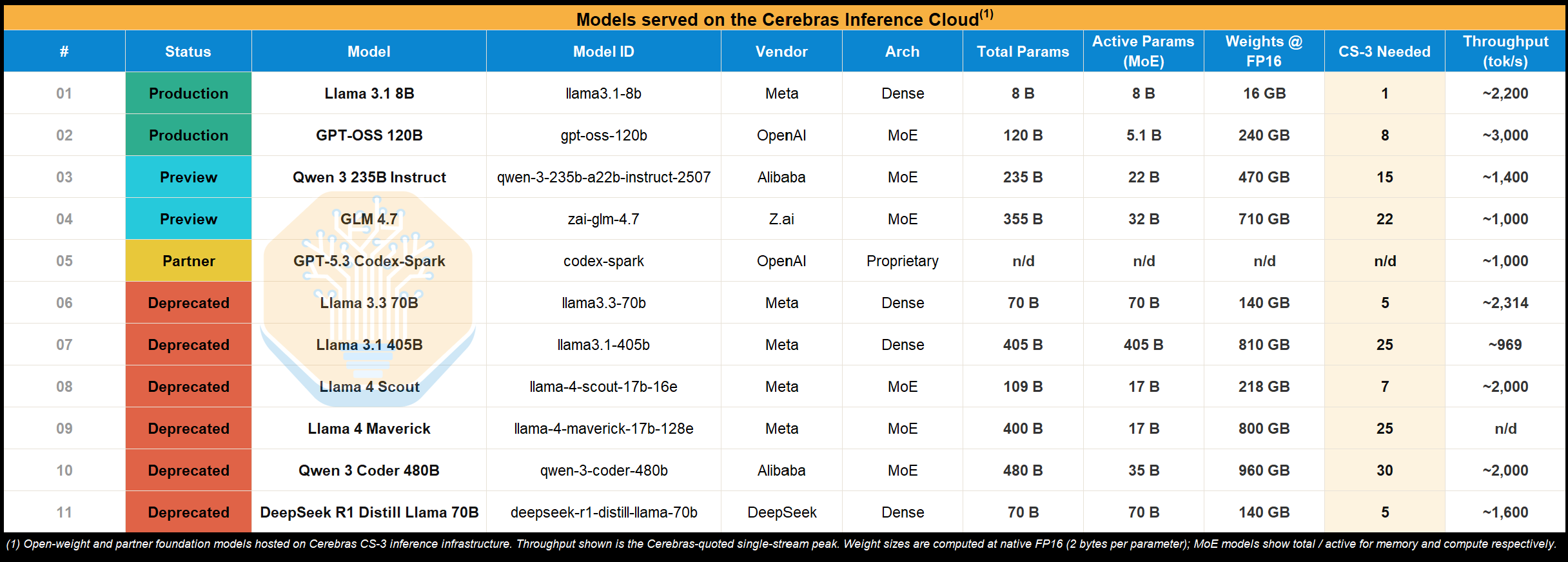
It’s also worth emphasizing that two of the most popular frontier open-source models of 2025, DeepSeek V3 and Kimi K2, have never been offered on the public Cerebras Cloud. This is despite the large KV cache size reduction in DeepSeek V3 due to the use of Multi-head Latent Attention (MLA), which would leave it with better serving economics than Llama 3 405B.
With that said, our analysis above shows that the even newer DeepSeek V4 Pro can have a similar deployment shape to Llama 405B (which they have already served on Cerebras cloud), with significantly smaller KV cache sizes. For that reason, with modern KV cache compression techniques and enough concurrency, Cerebras might indeed look attractive even for large 1T+ models.
The Cerebras OpenAI Deal
OpenAI plays a huge role in Cerebras’s future. It is simultaneously the company’s secured lender, its largest warrant holder, and the source of essentially all of its $24.6B backlog. OpenAI’s financial stake in Cerebras means Cerebras’s fortunes are tied to a single counterparty through three interlocking mechanisms that all move in the same direction. If the relationship succeeds, the loan is repaid through capacity delivery rather than cash (with the 6% accrued interest waived on capacity-repaid portions), the warrant vests and aligns incentives, and revenue scales into the billions. On a fully diluted basis, OpenAI could hold as much as 12% of Cerebras shares (not including any new issuances and offerings).
Here are the details:
· In December 2025, Cerebras and OpenAI signed a Master Relationship Agreement (MRA) under which OpenAI committed to purchase 750MW of AI inference compute capacity, deployed in tranches over 2026-2028, with each tranche carrying a 3-4 year term extendable to five years. OpenAI also holds an option (not an obligation) to purchase an additional 1.25GW, bringing the total potential to 2GW. The S-1 discloses $24.6B in remaining performance obligations as of December 31, 2025. More importantly, pass-through costs (data center rent, power, leasehold improvements, security) are reimbursed by OpenAI and recognized as revenue on a gross basis.
· OpenAI also provided a $1B Working Capital Loan to Cerebras via a secured promissory note that bears 6% annual interest. Interest is waived if Cerebras repays through delivery of compute capacity or hardware under the MRA. Repayment is scheduled in equal amortized installments over three years, starting after delivery of the final tranche of the initial 250MW. If the MRA is terminated for any reason other than OpenAI’s own material uncured breach, Cerebras may be required to immediately repay the full outstanding balance plus accrued interest. OpenAI also retains the right to direct the custodian bank to stop following Cerebras’s instructions on deploying the funds and instead control the disposition directly.
· Alongside the MRA, Cerebras issued OpenAI a warrant for 33,445,026 shares of Class N (non-voting) common stock at an exercise price of $0.00001 per share, effectively free. The warrant vests in three structurally distinct tranches: 4,459,337 shares vested immediately upon receipt of the $1bn Working Capital Loan in January 2026; 5,574,171 shares vest upon the earlier of Cerebras reaching a $40bn market capitalization or OAI hitting specified fee payment milestones under the MRA; and the remaining 23,411,518 shares vest in sub-tranches tied to capacity delivery, split between Committed Capacity (tied to firm delivery dates already in the MRA) and Additional Capacity (which vests only if OAI exercises its option to expand the deal to the full 2GW). Per S-1 filings, Cerebras assessed that the working capital loan tranche, the market capitalization / payment threshold tranche, and the Committed Capacity sub-tranche are probable of vesting, while the Additional Capacity sub-tranche is not probable (i.e. the 2GW expansion is not yet baseline). OAI also holds demand registration rights, meaning it can force Cerebras to register these shares for public resale at any time. The warrant expires December 24, 2035, or five business days after no binding commitments or payments remain under the MRA.
· Under ASC 505-50, equity given to a customer is treated as recognized as contra-revenue over the life of the commercial agreement, not at vesting and not at market value. The number is locked to the grant date fair value, regardless of where the stock trades later. Per S-1 filings, Cerebras values the warrants at $82.02 per share as of December 31, 2025, which serves as a useful proxy for grant date fair value for the OpenAI deal. Applying the $82.02 per share to the full ~33.4M shares, we get a theoretical maximum contra-revenue of ~$2.74bn or roughly 10% of the revenue expected from OpenAI. We assume the reported $24.6bn backlog is NET of the contra-revenue from the warrants. In reality, however, only the probable tranches flow through revenue on a sliding-scale basis; the Working Capital Loan tranche (~$366mn, vested January 2026), the market capitalization / payment threshold tranche (~$457mn), and the Committed Capacity sub-tranche (size undisclosed). The Additional Capacity sub-tranche only hits contra-revenue with a cumulative catch-up adjustment if and when OAI exercises the 2GW expansion option.
While Cerebras had been largely left out of the neocloud boom, OpenAI’s February release of GPT-5.3-Codex-Spark (a model using the gpt-oss-120B architecture that was distilled from the real 5.3 Codex) is turning things around. Spark runs on Cerebras at up to 2,000 tok/sec/user and led to the announcement of a long-term deal between the two companies, driving their IPO prospects (and the value of sama’s stake) ever higher.
Cerebras’s chips are only economically capable of serving relatively small models today, or at least based on what’s available to the public. GPT-5.3-Codex-Spark, for example, is NOT at all the same thing as the full GPT-5.3-Codex; it’s gpt-oss-120b fine-tuned on GPT-5.3-codex traces. In other words, it’s a distilled model that’s over 10x smaller.
While GPT-5.3-Codex-Spark is really fast, its tokens likely aren’t worth $10B today. For OpenAI to run any model above 1T total params with a 1M context window for modern agentic workload patterns, they will need to accept significant tradeoffs on cost (and recoup it by selling those tokens at a significant premium), and we expect the realized performance to be below 1000 tok/sec interactivity. On the other hand, algorithmic improvements will certainly make small models smarter. We’re probably less than a year away from GPT 5.5-level intelligence in a 120B form factor.
As mentioned earlier, many of our engineers were willing to forgo the frontier level intelligence of Opus 4.7 in exchange for faster tokens from Opus 4.6 fast. With GPT-5.5, OpenAI finally has an Opus 4.5 level model. Will people be willing to pay for really fast GPT-5.5- quality tokens a year from now even after the true bleeding edge frontier has moved far beyond it? For the first time ever, we think the answer may be yes. While the first 750MW is locked, there is much more upside for Cerebras if OAI chooses to take the full 2GW or even more. This is all dependent on the quality of the model they can fit on Cerebras hardware.
Behind the paywall, we will go through just how the OAI deal’s profitability Cerebras and the major execution risk - how far along is Cerebras in securing the DC capacity.