

Nvidia – The Inference Kingdom Expands
Groq LP30, LPX Rack, Attention FFN Disaggregation, Oberon & Kyber Updates, Nvidia's CPO Roadmap, Vera ETL256, CMX & STX
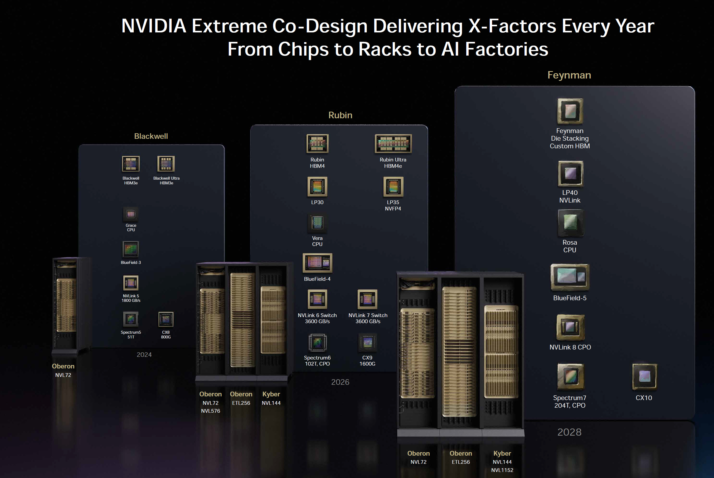
At GTC 2026, Nvidia delivered an event packed full of ground breaking announcements. Nvidia’s pace of innovation is not showing any signs of slowing, as they introduced three entirely new systems this year: Groq LPX, Vera ETL256, and STX. Also announced were updates to Nvidia’s Kyber rack architecture system, CPO making its debut for scale-up networking with the unveiling of the Rubin Ultra NVL576 and Feynman NVL1152 multi-rack systems. Early hints on Feynman’s architecture was also a key topic. A Jensen callout for InferenceX during the keynote was a highlight.
This is our GTC 2026 recap, and we will address many of the key questions that have been left unanswered by Nvidia. Specifically, we will go through the LPX rack and LP30 chip and explain how attention and feed forward network disaggregation (AFD) works; more details on the various rack architectures behind NVL144, NVL576, and NVL1152 and clarify just how much optics will be inserted as well as the rationale behind the dense Vera ETL256. The next generation Kyber rack had some big updates and some hidden details.
Groq
First up is the Groq LPU. One of the most significant recent events in AI infrastructure was Nvidia’s “acquisition” of Groq. Strictly speaking, Nvidia paid Groq $20B to license their IP and hire most the team. This functions almost as an acquisition, though its structure technically falls short of it being legally considered as one, thereby simplifying or obviating the need for regulatory approvals. Given Nvidia’s market share, if this transaction were structured as a full acquisition and were put to anti-trust review, such a transaction would likely not go through. The other benefit is that it avoids a drawn-out transaction closing process. Nvidia got instant access to Groq’s IP and people. This is why, less than four months after the deal was announced, Nvidia already has a system concept that is being integrated into the Vera Rubin inference stack.
Let’s now go through a refresher on the LPU architecture to see how Groq’s LPU complements Nvidia’s GPU. For more details see our original Groq piece. The premise from that piece remains unchanged: the standalone Groq LPU system is not economical for serving tokens at scale, but it can serve tokens very quickly which can demand a large market premium. This is the premise behind how LPU fits into a disaggregated decode system.
LPU chip
Groq’s first and only publicly announced LPU architecture was detailed in their ISCA 2020 paper. Unlike typical hardware architectures connecting many general-purpose cores, Groq re-organized the architecture into groups of single-purpose units connecting to other groups of different purposes, and they named the groups “slices.” Between functional units are streaming registers, scratchpad SRAM for functional units to pass data to each other. Groq opted for single-level scratchpad SRAM instead of multi-level memory hierarchy to make the hardware execution deterministic.
Concretely, LPU architecture has VXM slices for vector operations, MEM slices for loading/storing data, SXM slices for tensor shape manipulation, and MXM slices for performing matrix multiplication. Spatially, the slices are laid out horizontally, allowing the data to stream horizontally. Within a slice, instructions are pumped vertically across units. Conceptually, LPU resembles a systolic array that pumps instructions vertically and data horizontally.
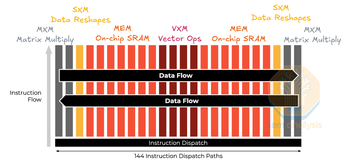
The data flow and instruction flow design requires fine-grained pipelining to achieve high performance. Since LPU architecture makes computation deterministic, the compiler can aggressively schedule and overlap instructions to hide latency. The LPU’s use of high bandwidth SRAM and aggressive pipelining are the two main factors that enable LPU’s low latency.
LPU gen 1 was designed on a legacy Global Foundries 14nm process, with Marvell responsible for the chip’s physical design. This was a much more mature node compared to peers when it taped out in 2020, with the incumbent AI chip platforms mostly on TSMC’s N7 platform. This made sense for an early product focused on proving out Groq’s architecture and bringing its inference-centric design to market. The 14nm node was mature, relatively well understood, and suitable for an initial chip where architectural differentiation mattered more than pushing its silicon to the leading edge.
One of the selling points is that the chip can be manufactured and packaged entirely in the United States compared to their competitors being heavily reliant on the Asia semiconductor supply chain: logic and packaging in Taiwan, with HBM from Korea.
Since then, Groq’s roadmap has stalled due to execution, with no LPU 2 having been shipped. This leaves the Groq LPU looking even more dated against competing roadmaps. What was once a meaningful but still manageable node disadvantage versus 7nm-era peers has widened into a far sharper gap, with all leading accelerator platforms now moving onto 3nm-class processes in 2026.
The follow on Groq LPU 2 was designed for Samsung Foundry’s SF4X node, specifically at Samsung’s Austin fab, allowing them to extend the pitch that Groq is fabricated domestically in the USA. Samsung would also provide support for the back-end design. The choice of Samsung was driven by favorable terms / investment, with Samsung Foundry struggling to find customers for its advanced nodes and missing out on an AI logic customer. Unsurprisingly, Samsung was a key investor in Groq’s subsequent Series D in August 2024, and most recently in September 2025 before the Nvidia “acquisition.”
However, the Groq LPU 2 was never productized because of design issues. The C2C SerDes on the chip couldn’t hit the advertised 112G speed which caused the design to malfunction, as we detailed long ago in the Accelerator model. The third generation Groq LPU is the one that Nvidia will be productizing.
SRAM and Memory Hierarchy
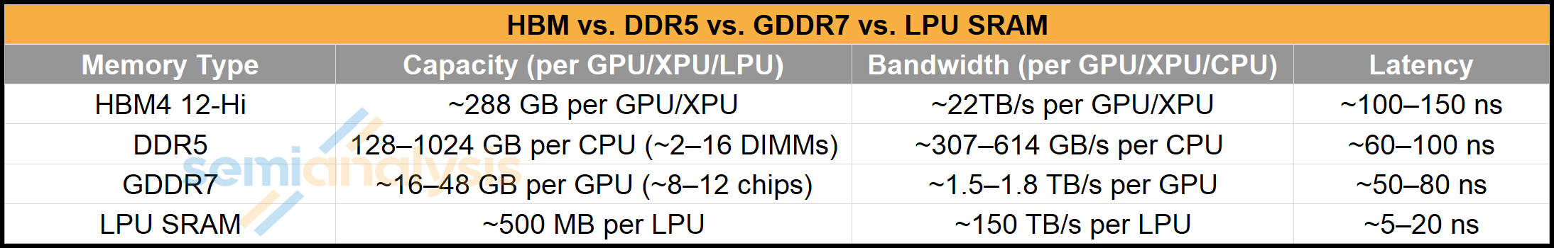
We have written about the role of SRAM in the memory hierarchy, but the quick recap is that SRAM is very fast (low latency and high bandwidth) but this comes at the expense of density and therefore cost.
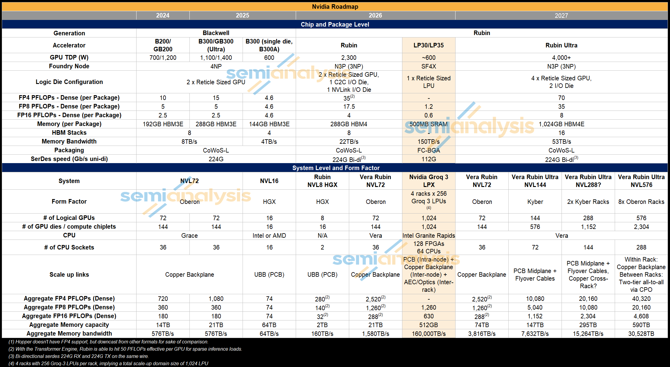
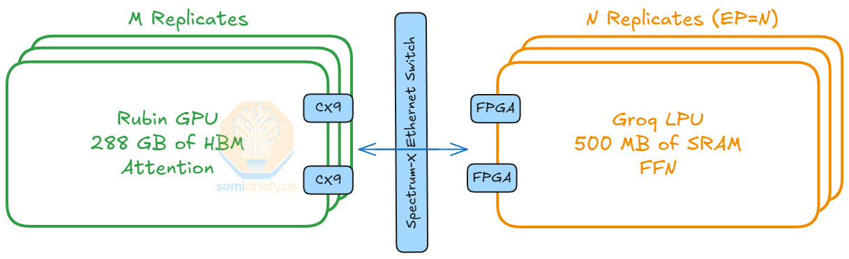
SRAM machines such as Groq’s LPU therefore enable very fast time to first token and tokens per second per user but at the expense of total throughput, as their limited SRAM capacity quickly gets saturated by weights, with little left over for KVcache that grows as more users are batched. GPUs win for throughput and cost as we have shown. This is why Nvidia has decided to combine these architectures to get the best of both worlds: accelerate parts of decode that are more latency sensitive and are not as memory heavy on a low-latency SRAM-heavy chip like the LPU, while memory hungry attention is performed on GPUs that come with a lot of fast (but not SRAM fast) memory capacity.
This brings us to the Groq 3 LPU or LP30, with LPU gen 2 being skipped over. This chip has no Nvidia design involvement. The SerDes issues affecting v2 appear to be fixed. Behind the paywall, we will reveal the SerDes IP vendor which may come as a surprise. Nvidia also announced an LP35 which is a minor refresh of the LP30 which will remain on SF4 and will require a new tapeout. It will incorporate NVFP4 number format but given Nvidia is prioritizing time to market we don’t expect any other drastic design changes.
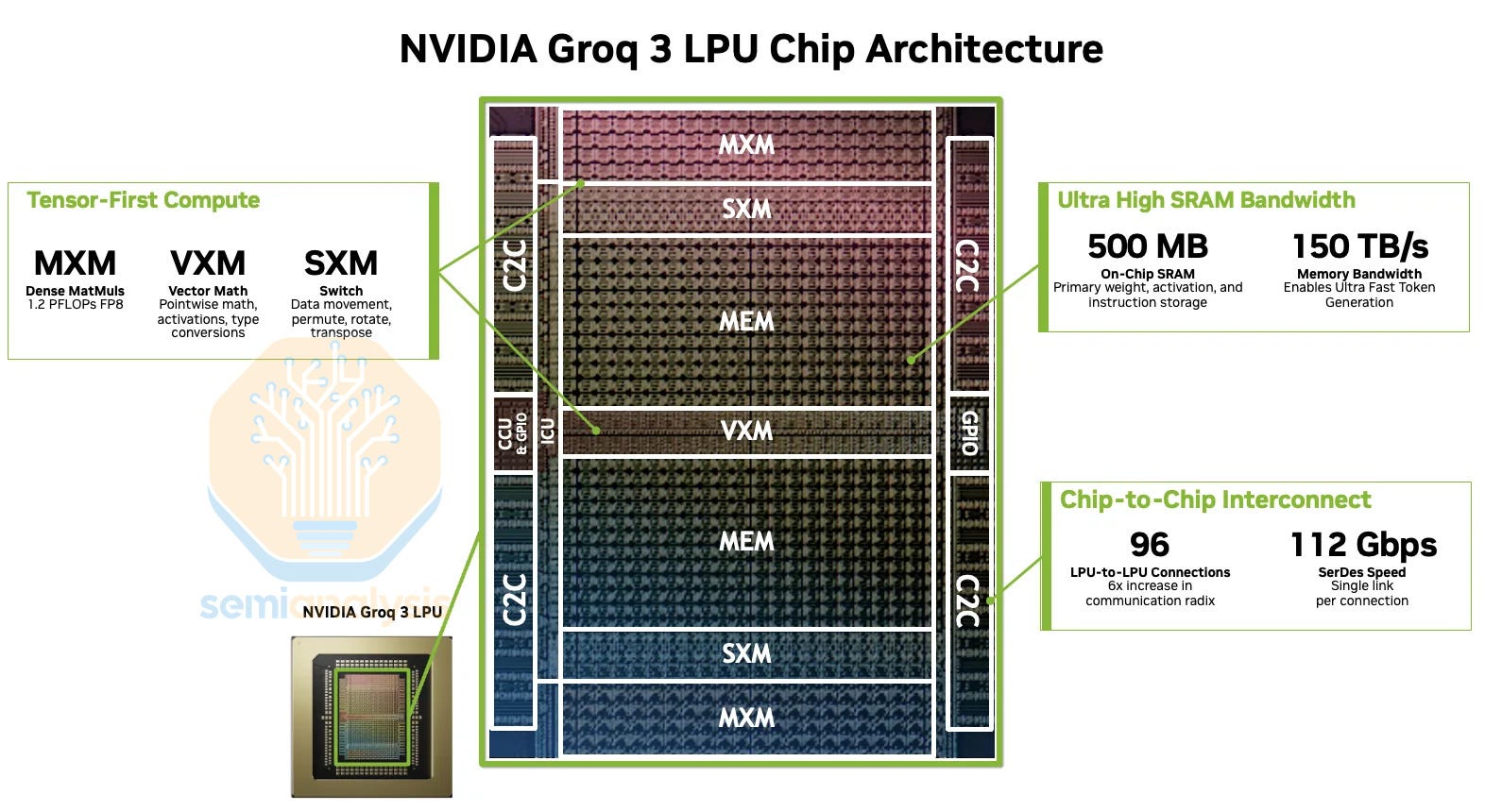
LPU 3’s near reticle size die layout is very similar to LPU 1. a significant amount of area taken is up by the 500MB of on-chip SRAM, with a very small amount of area dedicated to MatMul cores that offer 1.2 PFLOPs of FP8 compute – a fraction of compute compared to Nvidia GPUs. This compares to LPU 1 with 230MB of SRAM and 750 TFLOPs of INT8, with the performance increase mostly driven by node migration from GF16 to SF4. As a single monolithic die, advanced packaging isn’t required.
One of the benefits of relying on SF4 is that it isn’t constrained like TSMC’s N3, which is putting a cap on accelerator production and is a key reason why the industry remains compute constrained. This is in addition to not having HBM which is also constrained. This allows Nvidia to ramp production of the LPU without sacrificing or eating into their valuable TSMC allocation or HBM allocations, representing true incremental revenue and capacity that noone else can access.
Since Nvidia has taken over, the next generation LP40 will be fabricated on TSMC N3P and use CoWoS-R, and Nvidia will contribute more of their own IP such as supporting the NVLink protocol rather than Groq’s C2C. This will be the first LPU to be extremely co-designed alongside the Feynman platform. Groq’s original plans for LPU Gen 4 was also with TSMC and Alchip as the back-end design partner. Alchip’s involvement is now redundant with Nvidia able to perform backend design on their own. One of the technical innovations planned is hybrid bonded DRAM to extend on-chip memory with only a slight decrease in latency and bandwidth vs SRAM, but much higher performance compared to DRAM. SK Hynix was tapped as the supplier of the DRAM to be used for the 3D stacking. All of this and more was detailed long ago in the Accelerator model.
GPU and LPU Integration: Attention FFN Disaggregation (AFD)
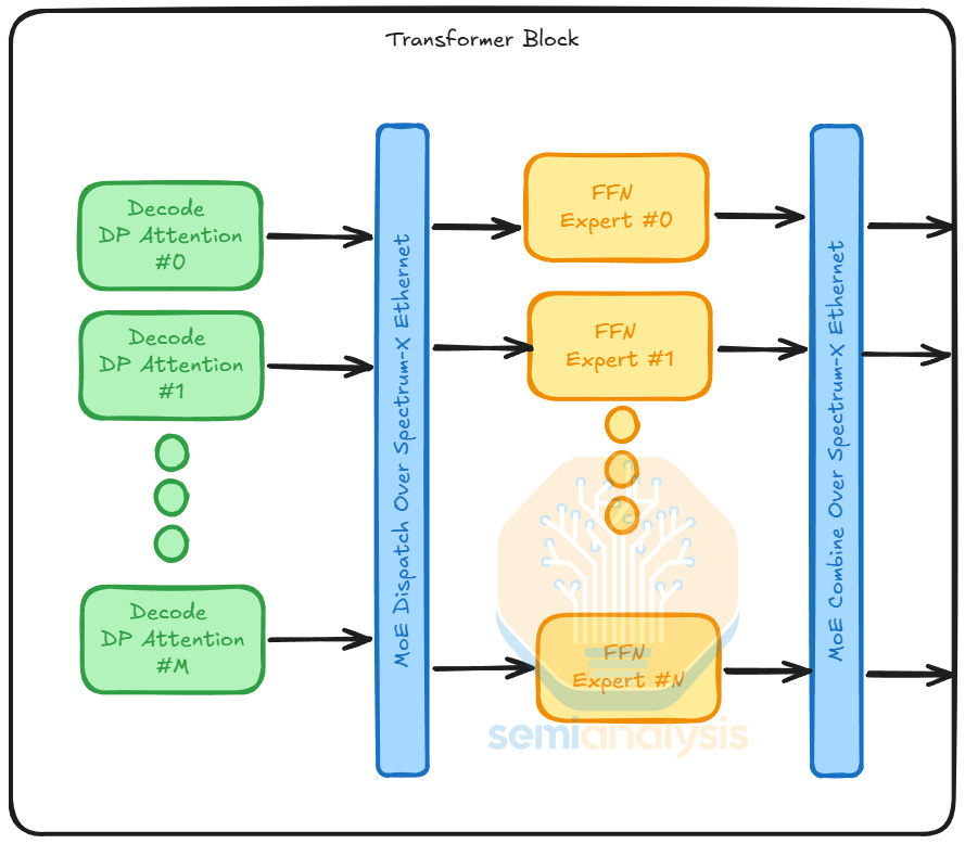
Now with an understanding of what LPUs are good for we can understand how they fit into inference setups. NVIDIA introduced LPUs to improve the performance of high interactivity scenarios. In those scenarios, LPUs can leverage their low-latency capabilities to improve the decode phase latencies. One way LPUs can improve decode phase latencies is by applying the Attention FFN Disaggregation (AFD) technique, introduced in MegaScale-Infer and Step-3.
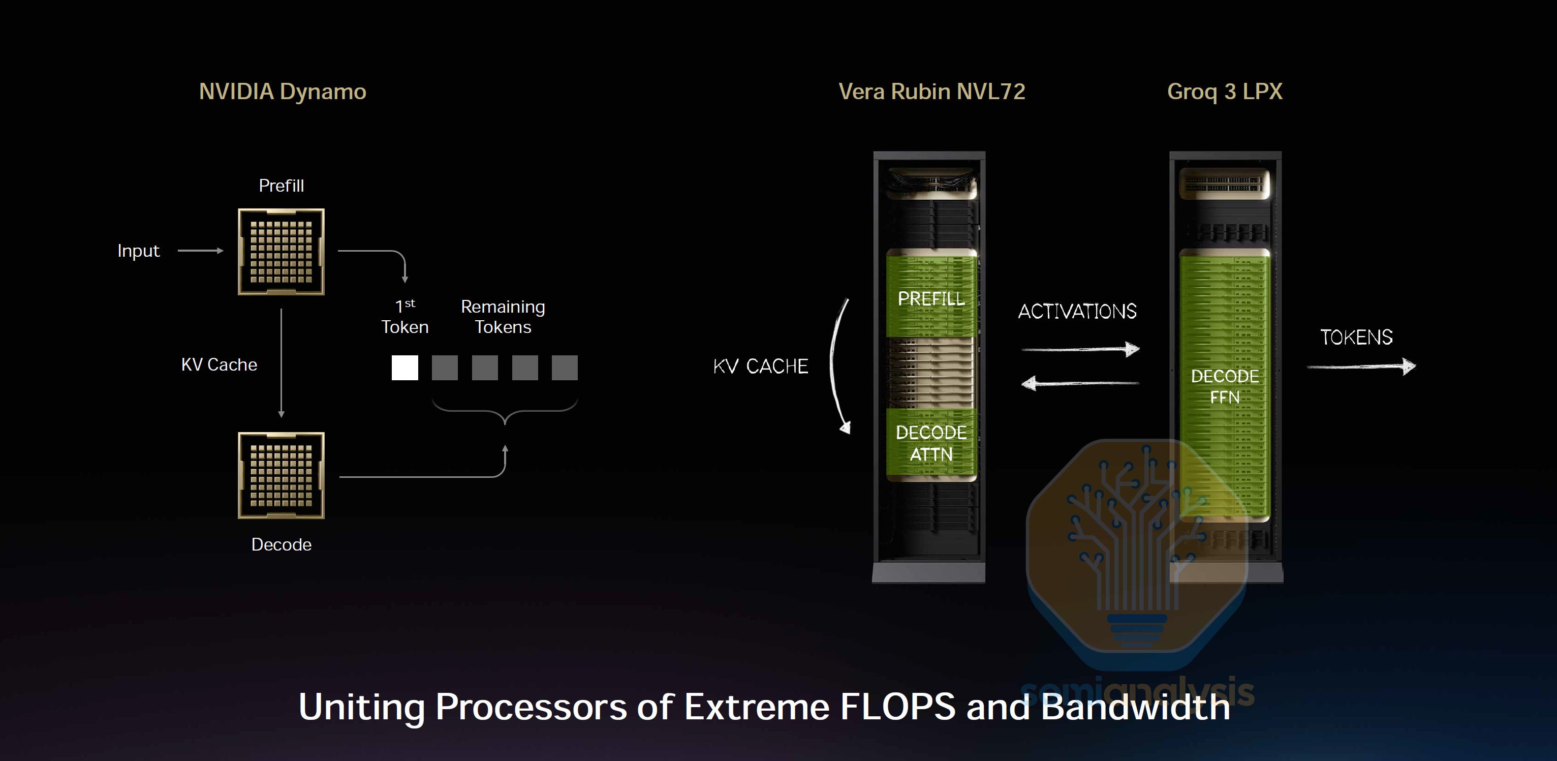
As we explained in our InferenceX article, LLM inference involves two phases: prefill and decode. Prefill processes the full input context: It is compute-intensive, which is suitable for GPUs. On the other hand, decode predicts new tokens and is memory-bounded. Decode is latency-sensitive because the model predicts new tokens one by one, and LPU’s high SRAM bandwidth and low-latency capabilities can help accelerate this iterative process.
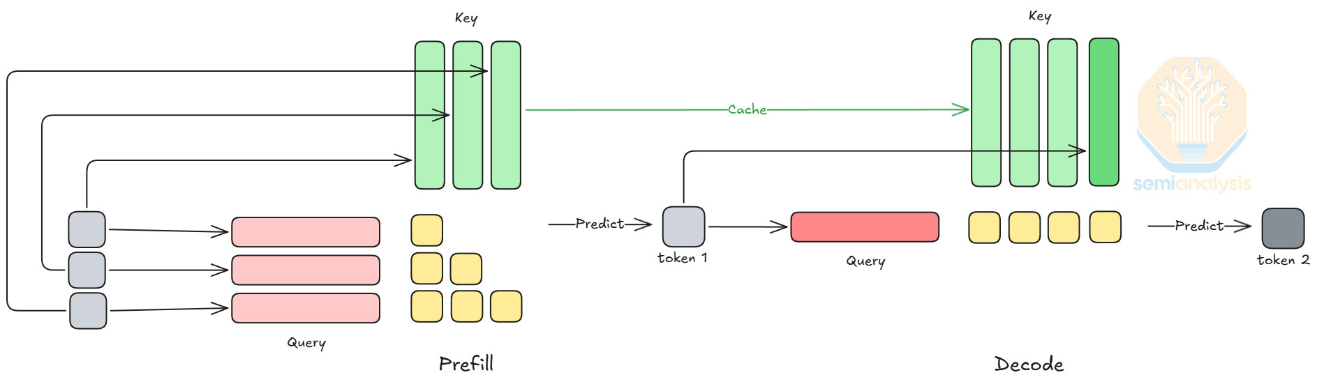
Attention and FFN are subsets of operations in a model. In a model forward pass, attention’s output feeds into a token router, and the token router assigns each token to k experts, where each expert is an FFN. Attention and FFN have very different performance properties. During decode phase, the GPU utilization of attention barely improves when scaling batch size due to being bounded by loading KV cache. In contrast, the GPU utilization of FFN scales with batch size comparatively better.
This is something we have worked with certain hardware vendors and memory companies on with our inference simulator for more than 6 months.
As state-of-the-art mixture-of-expert (MoE) models grow increasingly sparse, tokens can choose experts from a larger expert pool. As a result, each expert receives fewer tokens, leading to lower utilization. This motivates attention and FFN disaggregation. If a GPU only performs attention operations, its HBM capacity can be fully allocated to KV cache, increasing the total number of tokens it can process, which then increases the tokens each expert processes on average.
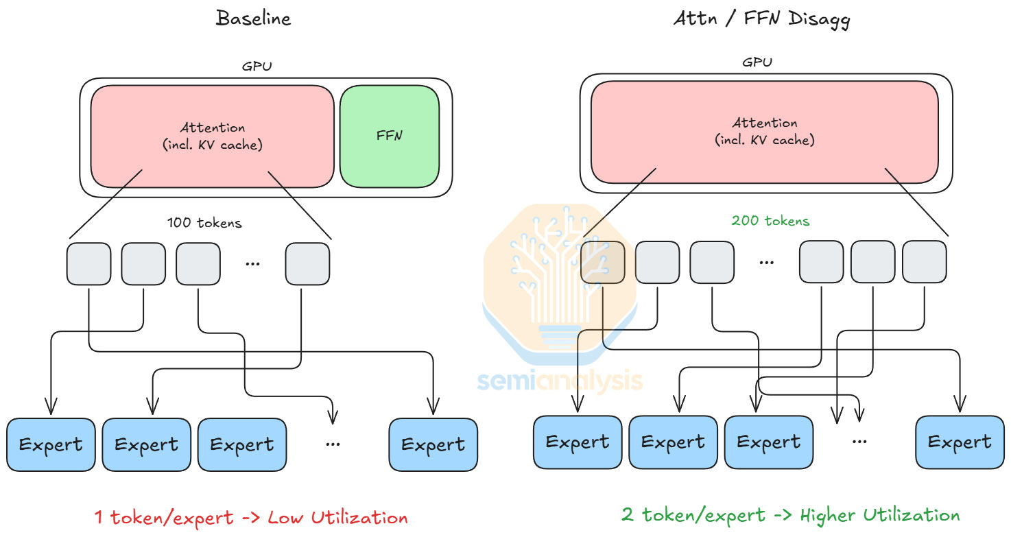
Comparing the two operations, we see attention is stateful due to dynamic KV cache loading patterns, whereas FFN is stateless since the computation only depends on the token inputs. Thus, we disaggregate the computation of attention and FFN. We map attention computations to GPUs, which handle dynamic workloads well. For FFNs, we map them to LPUs, since LPU architecture is inherently deterministic and benefits from static compute workloads.
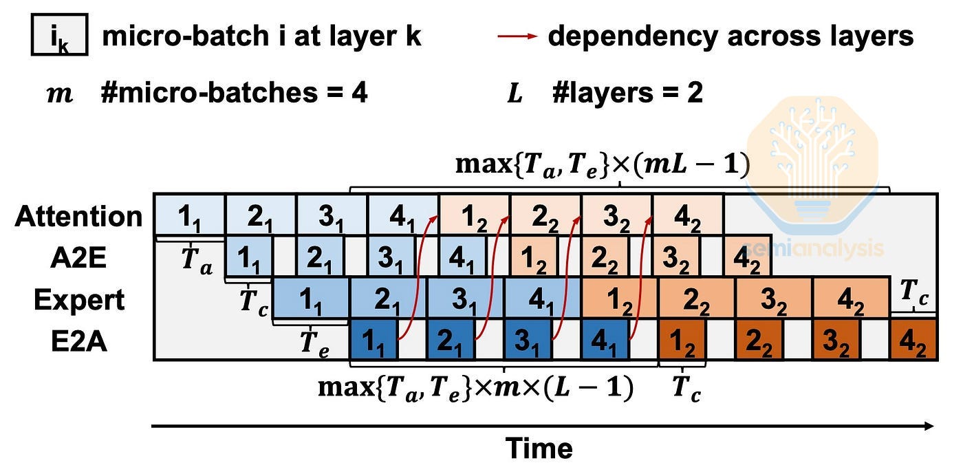
With AFD, token routing from GPUs to LPUs can become the bottleneck, especially under strict latency constraints. The token routing flow involves two operations: dispatch and combine. In the dispatch step, we route each token to their top k experts with an All-to-All collective operation. After experts complete their computation, we perform the combine step, where the outputs are sent back to the source location with a reverse All-to-All collective, continuing the next layer’s computation.
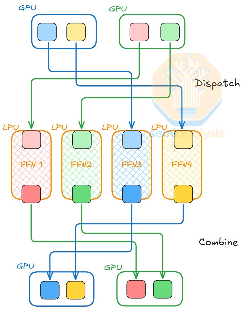
To hide the communication latency of dispatch and combine, we employ ping pong pipeline parallelism. In addition to splitting batches into micro-batches and computation pipelining like standard pipeline parallelism, the tokens dispatched to the LPUs are combined back to the source GPUs, so they ping pong between the GPUs and the LPUs.
Speculative Decoding
A different way LPUs could improve decode phase latencies is by accelerating a speculative decoding setup, where we deploy draft models or Multi-Token Prediction (MTP) layers onto LPUs.
For a decoding step of context N tokens, adding k additional tokens during forward pass (a warm prefill of k new tokens) marginally increases the latency when k << N. Using this property, speculative decoding uses a small draft model or MTP layers to predict k new tokens, saving time since small models have lower latency per decode step. To verify the draft tokens, the main model only needs one warm prefill of k new tokens, at the latency cost of roughly a single decode step. Speculative decoding usually boosts output token per decode step by 1.5 to 2 tokens, depending on the draft model / MTP accuracy. With its low latency capabilities, LPUs can further increase the latency savings and improve throughput.
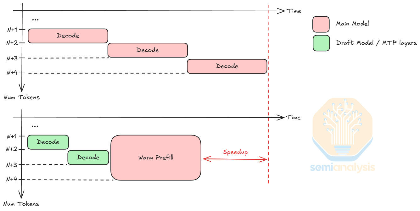
For LPUs, deploying a draft model or MTP layers is quite different from applying AFD. FFNs are stateless, while draft models and MTP layers require dynamic KV cache loading. Each FFN is around hundreds of megabytes, whereas draft models and MTP layers take up tens of gigabytes. To support this memory usage, LPUs can access up to 256 GB of DDR5 per Fabric Expansion Logic FPGAs on the LPX compute tray.
LPX Rack System
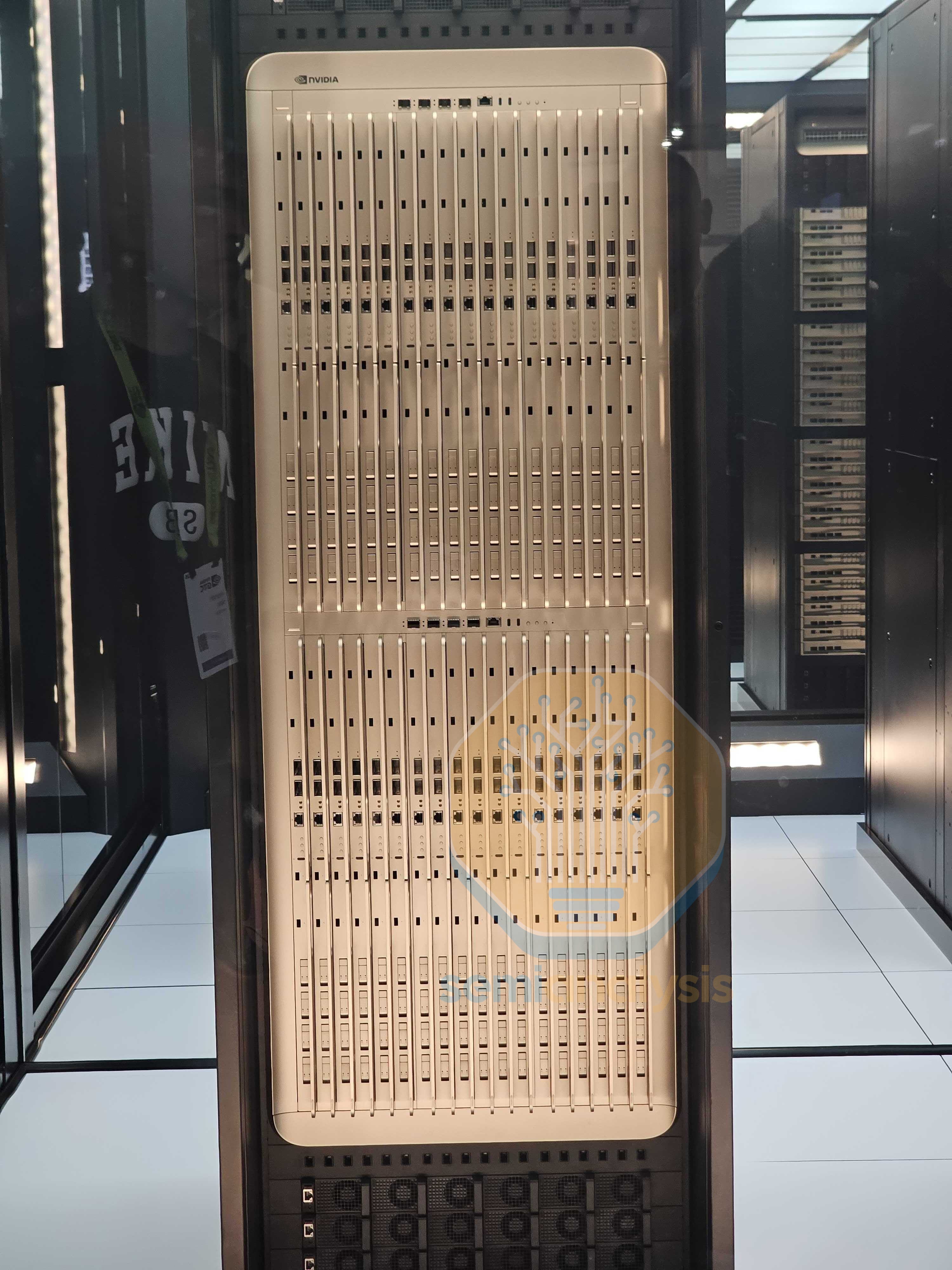
Let’s look at the LPX rack system, which has interesting details. Nvidia has displayed an LPX rack with 32 1U LPU compute trays with 2 Spectrum-X switches. This 32 tray 1U version that Nvidia has shown off at GTC is very close to Groq’s original server design before the acquisition. We believe that this server configuration is not the version that will be shipped in 3Q, with Nvidia implementing changes. Here, we will detail what we know about the actual production version. This was already detailed in the Accelerator model.
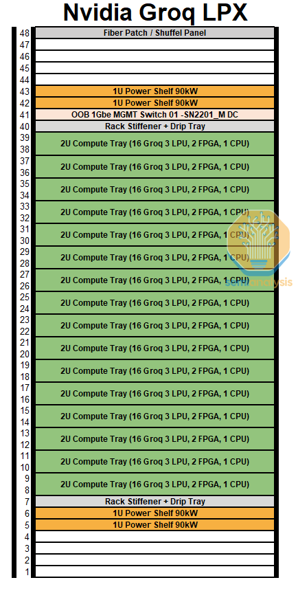
LPX Compute Tray
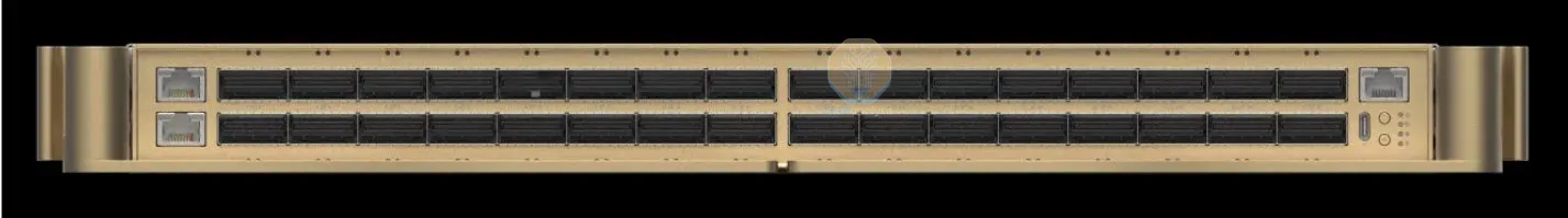
Each LPX compute tray or node has 16 LPUs with 2 Altera FPGAs, 1 Intel Granite Rapids host CPU and 1 BlueField-4 front-end module. As with other Nvidia systems, hyperscalers customers can and will use their own Front-end NIC of choice rather than paying for Nvidia’s BlueField.
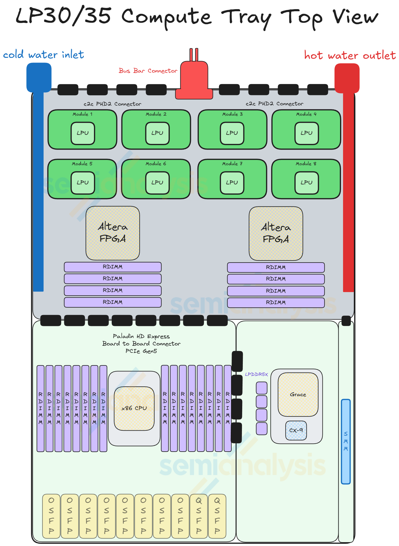
The LPU modules are mounted in a belly-to-belly on the PCB, meaning 8 LP30 modules on the top side of the PCB and the other 8 LP30 modules on the bottom. All of the connectivity that comes out of the LPU are via PCB traces and given the dense all-to-all mesh for intra-node connections this requires a very high spec PCB to support the routing. The belly-to-belly mounting is used to reduce PCB trace lengths across the ‘X’ and ‘Y’ dimensions.
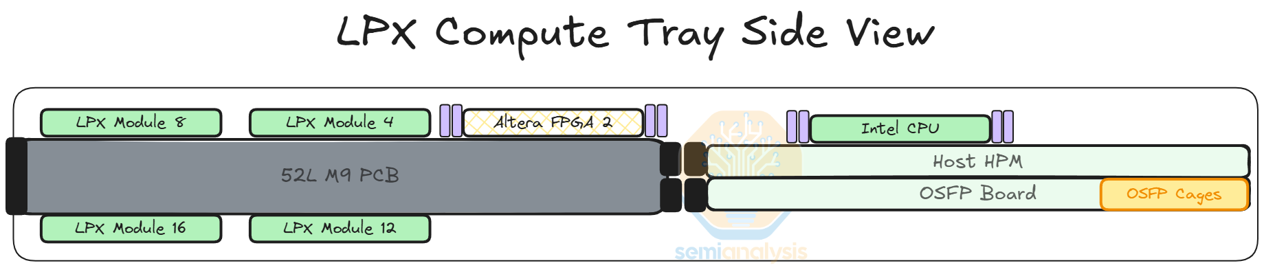
Something interesting about the system is the important role the FPGAs play. Nvidia refers to the FPGAs as “Fabric Expansion Logic” which serves multiple purposes. First, they act as a NIC which converts the LPU’s C2C protocol into Ethernet to connect to the Spectrum-X based ethernet scale-out fabric. It is this scale-out fabric through which the LPUs connect to GPUs in the decode system.
Second, the LPUs also traverse through the FPGAs to reach the host CPU, with the FPGAs converting C2C to PCIe to the CPU.
Third, the FPGAs are connected to the backplane to talk to other FPGAs in the node, we believe this is to help manage control flow and timing of all the LPUs. The FPGAs also bring extra system DRAM of up to 256GB each. This pool of memory can be used for KVCache if the user wants the entire decode process served by the LPX.
On the front panel there are 8 x OSFP cages for cross-rack C2C, while there will be 2 cages (likely QSFP-DD) that goes to the Spectrum-switches that is used to connect the LPUs and the GPUs for the disaggregated decode system. We will share more about this when we describe the network.
LPU Network
The LPU network can be divided into the scale-up ‘C2C’ network and scale-out network which interacts with the Nvidia GPUs through Spectrum-X. First let’s discuss the scale-up network which can be divided into 3 portions: intra-node, inter-node/intra-rack, inter-rack. For C2C within the rack Nvidia announced a total of 640TB/s of scale up bandwidth per rack which comes from 256 LPUs x 90 lanes x 112Gbps/8 x 2 directions = 645TB/s. Note that Nvidia uses the total 112G line rate rather than 100G of effective data rate.
Intra-Tray Topology
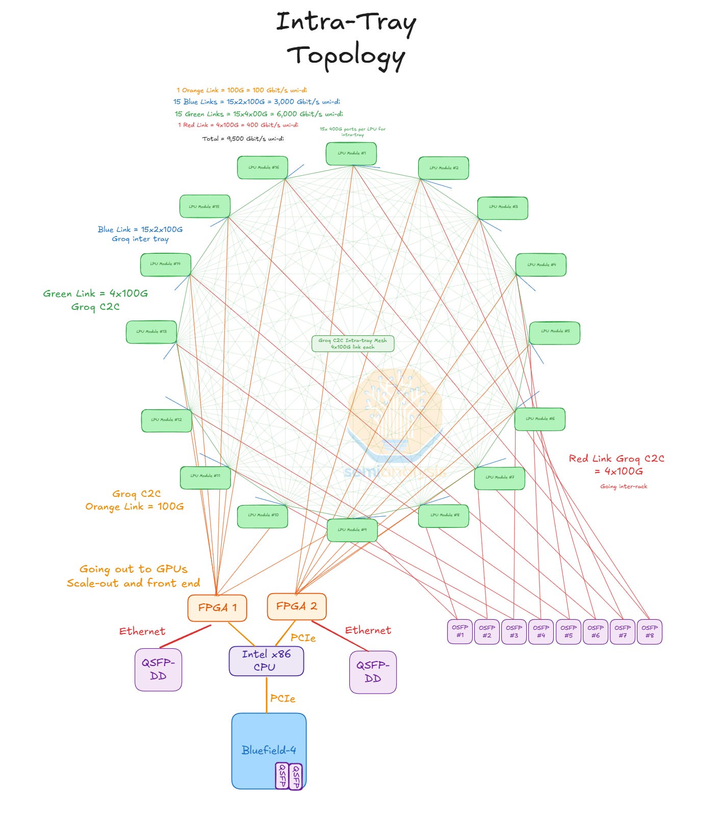
Within each tray or node, all 16 LPUs are connected to each other in an all-to-all mesh. Each LPU module connects to the 15 other LPUs within the node with 4x100G of C2C bandwidth. Note that this ‘C2C’ is not related to NVLink, but Groq’s own scaleup fabric. These connections are all via PCB trace, which necessitates an extremely high spec PCB to support this routing density. This is why the belly-to-belly layout is used: it reduces the ‘X’ and ‘Y’ distance between all the LPUs and instead have routing go in the ‘Z’ dimension.
The LPU also has 1x100G going to one FPGA, with each FPGA interfacing with 8 LPUs. The 2 FPGAs each have 8x PCIe Gen 5 going to the CPUs. The LPU needs to traverse through the FPGA to interface with the CPU as LPUs don’t have PCIe PHYs to interface directly.
Inter-node/Intra-rack
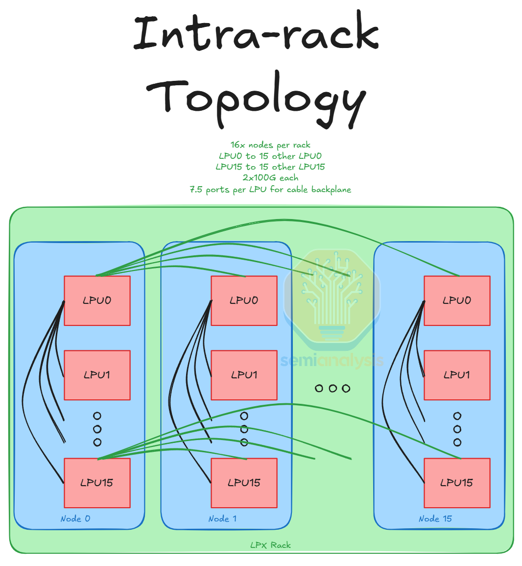
Each LPU connects to one LPU from each of the 15 other nodes in the server. Each of these inter-node links is 2x100G so there are 15x2x100G inter-node links coming out of each LPU. These inter-node links are via a copper cable backplane. In addition, each FPGA also connects to an FPGA in every other node at either 25G or 50G per link for 15x25G/50G. This also goes through the backplane. This means that each node has 16 x 15 x 2 lanes for inter-node C2C and 2 x 15 lanes for inter-node FPGA which is a total of 510 lanes or 1020 differential pairs (for Rx and Tx). Therefore, the backplane is 16 x 1020/2 = 8,160 differential pairs – we divide by 2 as each device Tx channel is a corresponding device’s Rx channel.
Inter-rack
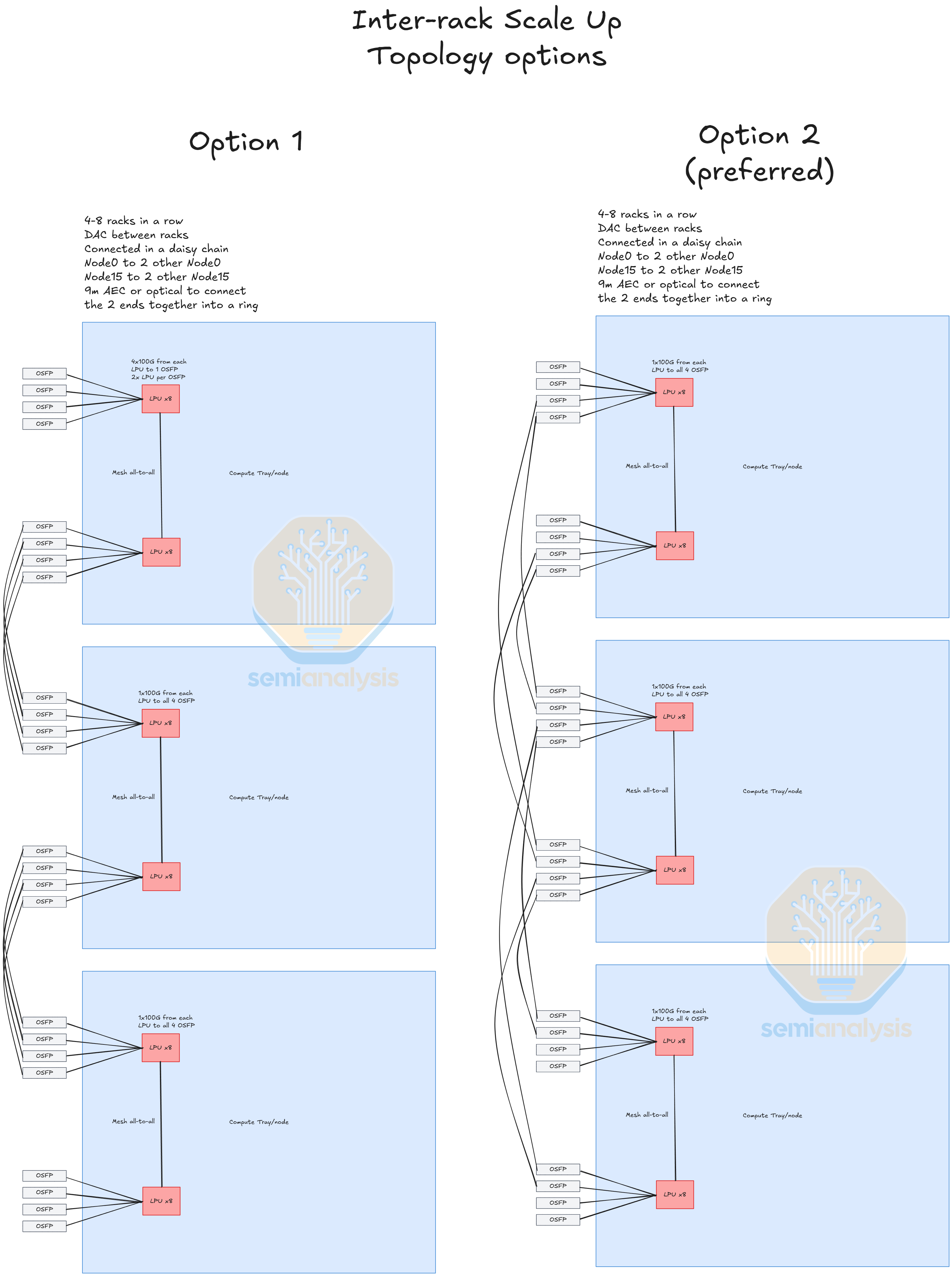
Lastly, there is the inter-rack C2C. Each LPU has 4x100G lanes that go to the OSFP cages to connect LPUs across 4 racks. There are various configurations that can be used for this inter-rack scale up. One option is 4x100G from each LPU going to one OSFP cage, each OSFP escaping 800G of C2C from 2 LPUs. However, for greater fan out the preferred configuration seems to be each 100G lane from the LPU going to 4 individual cages, with each cage escaping 800G of C2C from 8 LPUs. In terms of how the racks are networked together it appears to be a daisy chain configuration, with each Node0 connected to 2 other Node 0. This can all be achieved within the reach of 100G AECs, though optics can be used if necessary.
Nvidia’s CPO Roadmap
NVIDIA revealed its CPO Roadmap at the GTC Keynote 2026, with Jensen following up with additional commentary in the Financial Analyst Q+A meeting held the following day. Though many had their hopes up for CPO to be used for scale-up within the rack for Rubin Ultra Kyber, Nvidia’s focus was instead on using CPO to enable larger world size compute systems.
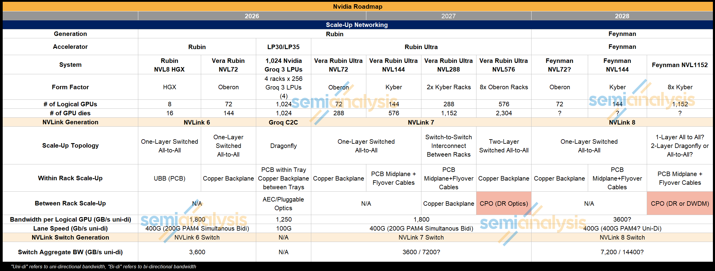
In the Rubin Generation, Nvidia will offer the Rubin GPU in an Oberon NVL72 form factor with an all-copper scale-up network. For Rubin Ultra, as we expected, there will only be a copper scale-up option for Rubin Ultra in the Oberon and Kyber Rack form factor. Rubin Ultra will also be offered in a larger world size system that connects 8 Oberon Racks of 72 Rubin Ultra GPUs to form what will be referred to as NVL576. CPO scale-up will be used to build the larger world size, connecting between the racks in a two-tier all to all network, though scale-up inside the racks will remain copper-based.
When we reach the Feynman Generation, CPO usage will expand via another large world size rack, the NVL1152 which is formed by combining 8 Kyber racks. While the Nvidia Technical Blog that outlines the rack configuration roadmap states that “NVIDIA Kyber will scale up into a massive all-to-all NVL1152 supercomputer using similar direct optical interconnects for rack-to-rack scale-up”, Jensen Huang in a Financial Analyst Q+A session did say that NVL1152 in Feynman would be “all CPO”. There is some disagreement on whether copper will still be used for scale-up within the rack or whether CPO will replace copper.
Nvidia’s approach has been to use copper where they can, and optics where they must. The architecture of NVL1152 in the Feynman generation will follow the same principle. It is clear that the NVL1152 will adopt CPO to connect between racks, but from GPUs to NVLink Switches is currently copper POR. Nvidia is unable to achieve another doubling of electrical lane speed from 224Gbit/s bi-di to 448Gbit/s uni-di means bandwidth isn’t that amazing.
While 448G high speed SerDes have big challenges for shoreline, reach, and power versus using a die-to-die connection to an optical engine, the manufacturing challenges, cost, and reliability for Feynman necessitate using copper to the Switch.
With that said, the NVL1152 SKU is years out – and the roadmap is highly likely to shift. For now, our base case stands at copper being used within each rack and CPO between the racks, but this could easily change.
For now – our best estimate of Nvidia’s CPO roadmap is as follows:
Rubin:
NVL72 – Oberon all copper scale up
Rubin Ultra:
NVL72 – Oberon all copper scale up
NVL144 – Kyber rack all copper scale up
NVL288 – Kyber rack all copper scale up with copper connecting 2 racks together
NVL576 – 8x Oberon Racks copper scale up within rack and CPO on switch between racks in a two tier all to all topology. This would be low volume for test purposes
Feynman:
NVL72 – Oberon Rack – All Copper
NVL144 – Kyber Rack – All Copper
NVL1152 – 8xKyber Rack – Copper within rack and CPO on the switch between racks

Source: SemiAnalysis, Nvidia
Oberon and Kyber Updates, Larger World Sizes Introduced, More Networking Updates
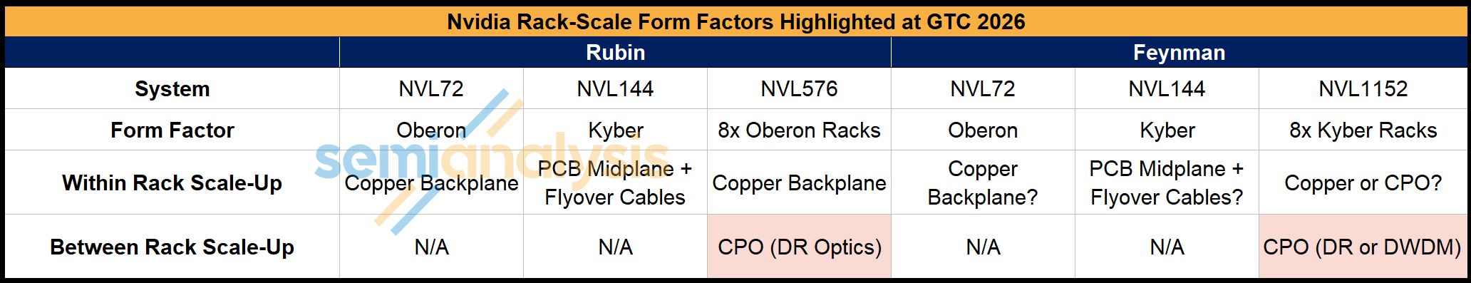
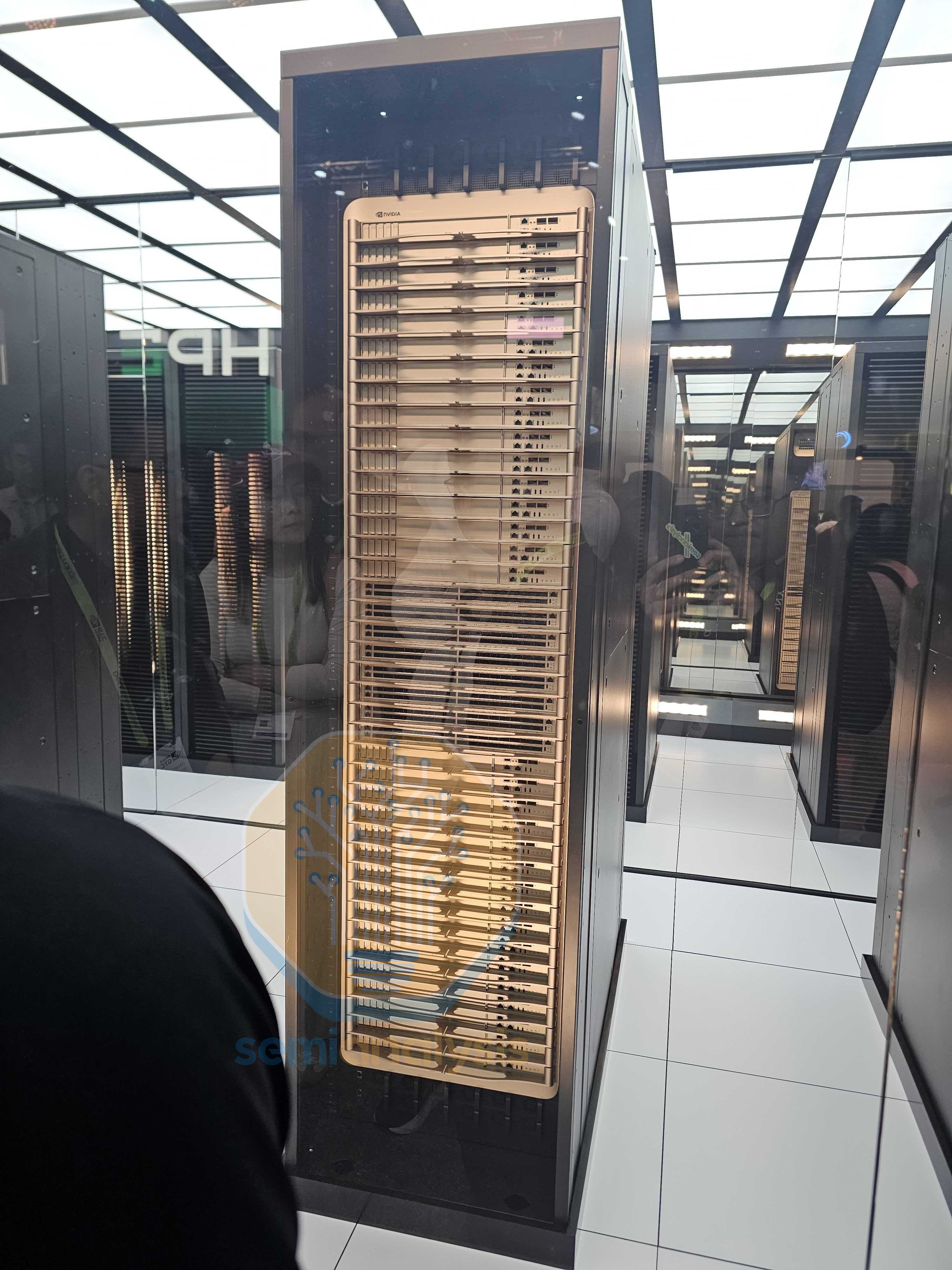
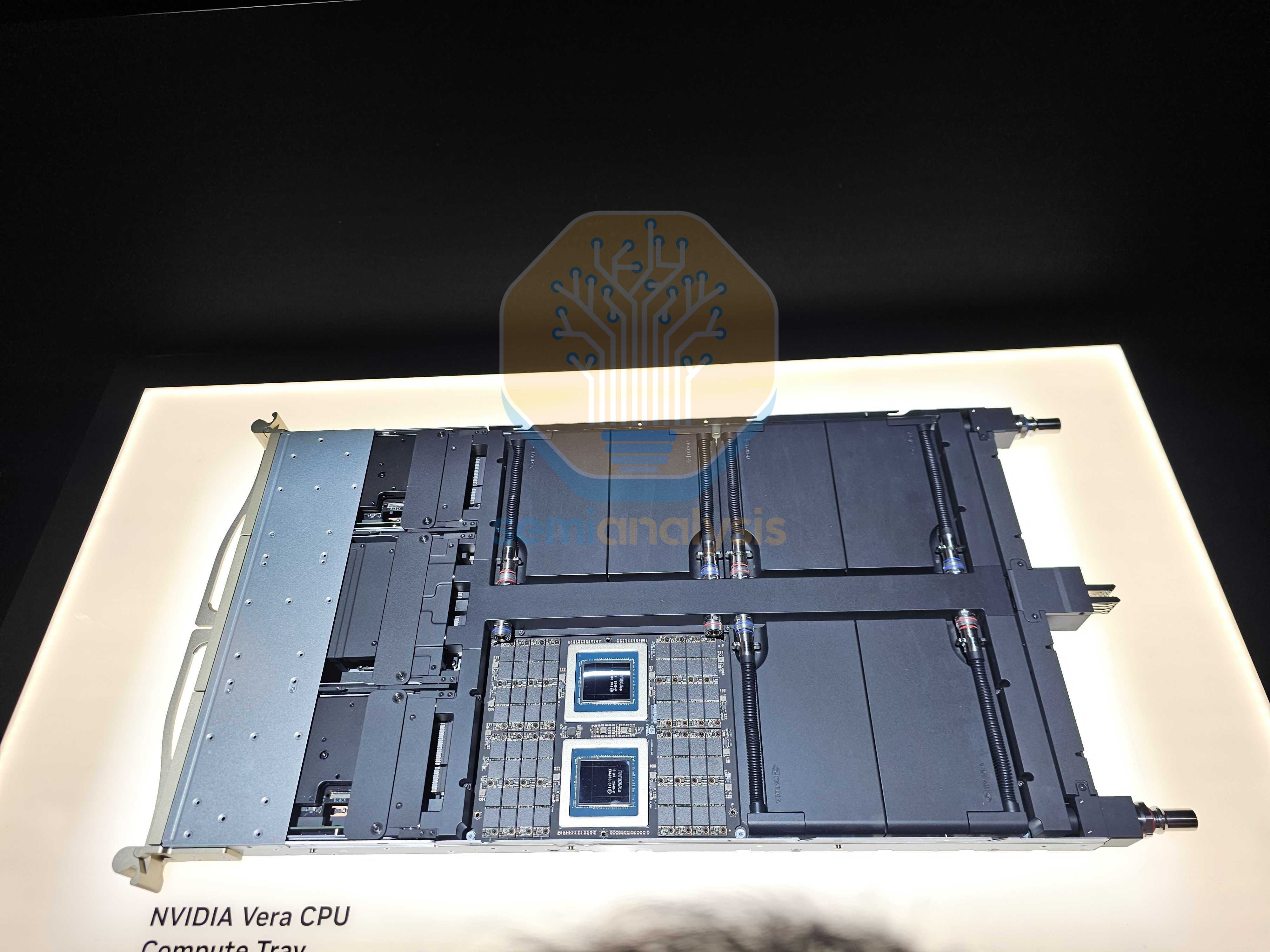
Nvidia provided a long-awaited update on its Kyber rack form factor, the latest addition to the lineup after Oberon having first been previewed as a prototype at GTC 2025. As a prototype, the rack architecture has continued to evolve, and we notice some changes. First, each compute blade has densified, with 4x Rubin Ultra GPU and 2x Vera each. There are a total of 2 canisters of 18 compute blades which amounts to 36 compute blades total for 144 GPUs in a rack. The initial Kyber design featured 2 GPUs and 2 Vera CPUs in one compute blade, with a total of 4 canisters of 18 compute blades each.
The details below are based on the Rubin Kyber prototypes, but Rubin Ultra will be redone.
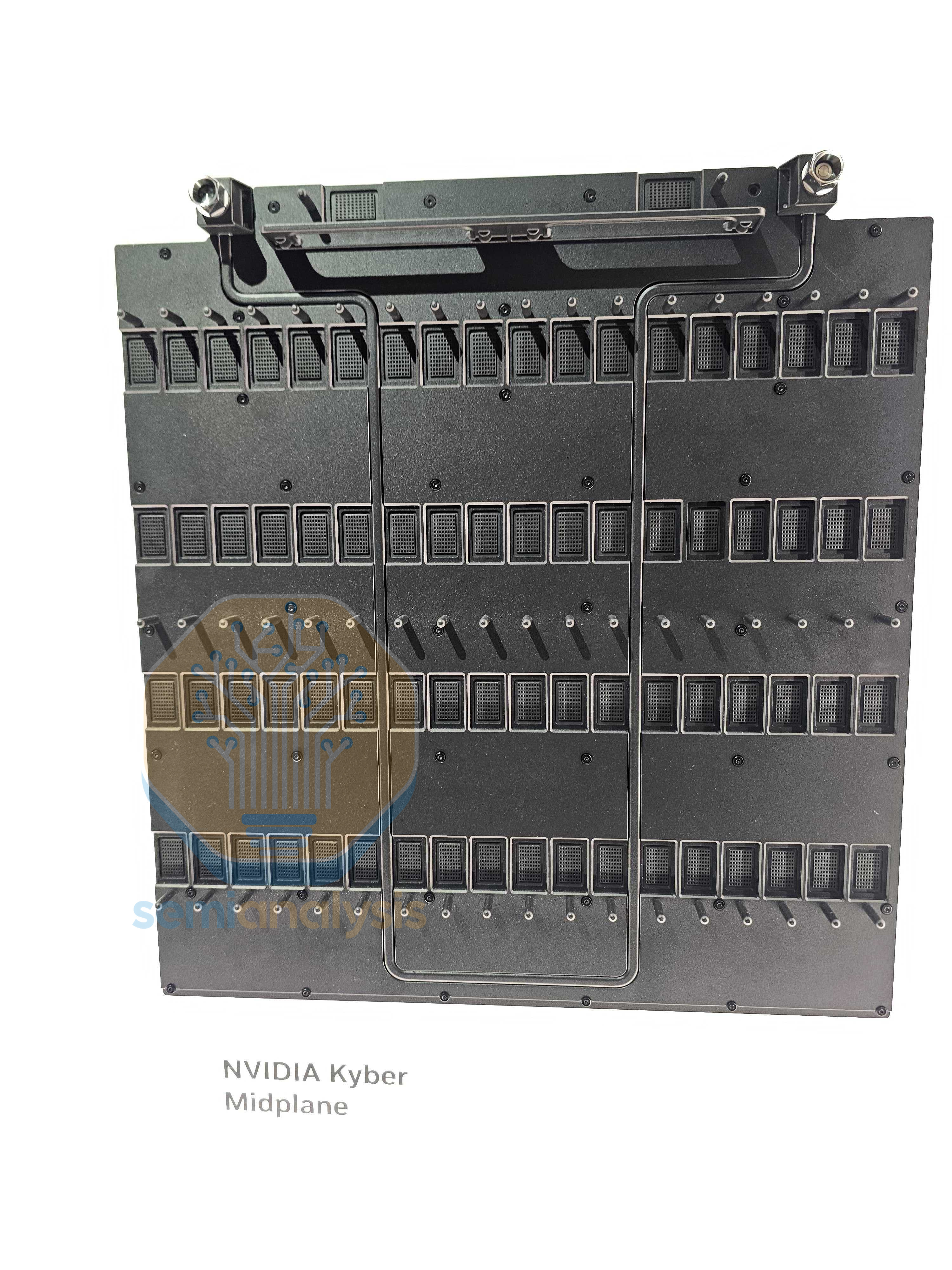
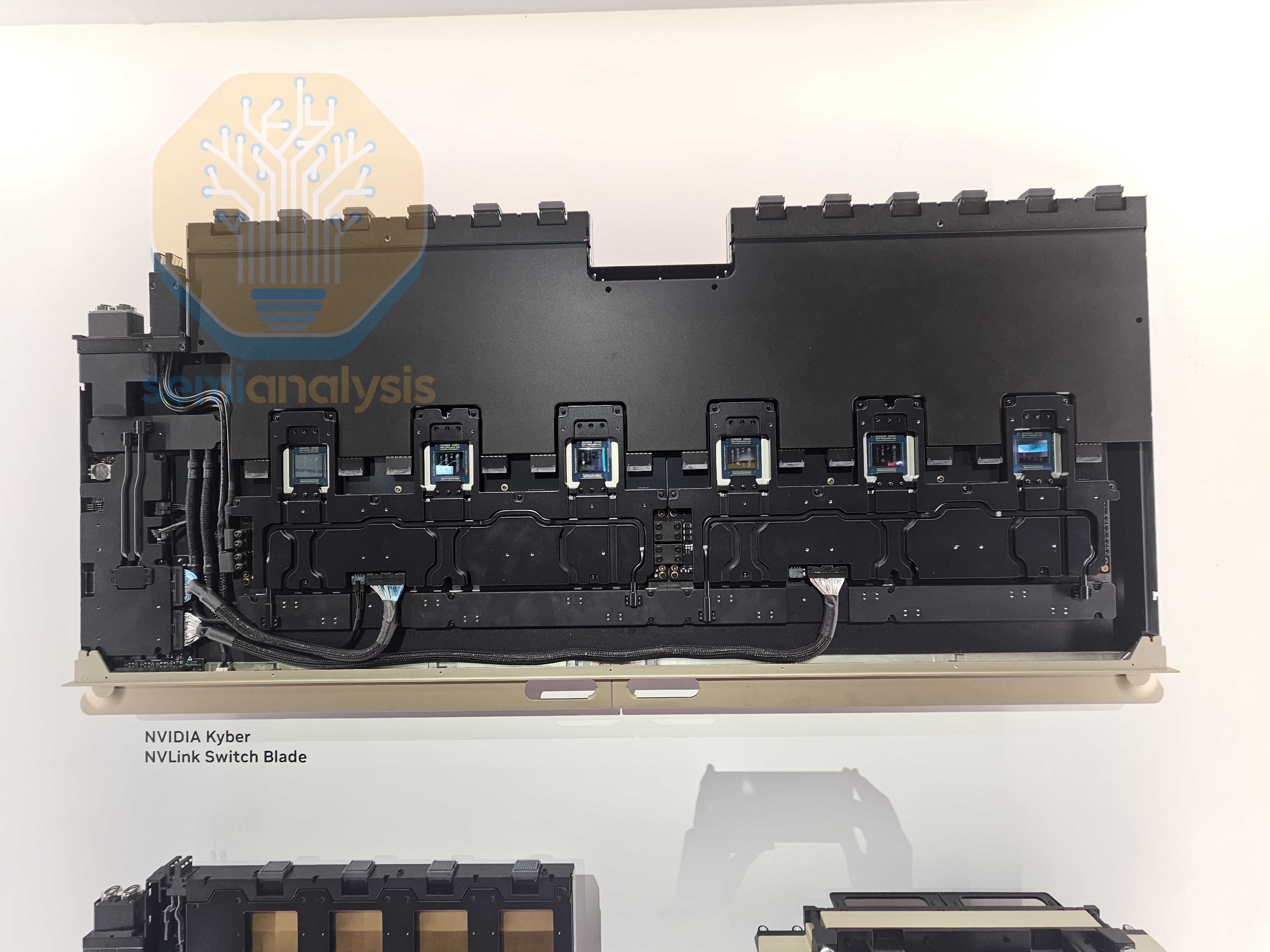
Each switch blade is also double in height vs the GTC 2025 prototype, with 6 NVLink 7 switches per switch blade, and 12 switch blades per rack, amounting to a total of 72 NVLink 7 switches per Kyber rack. The GPUs are connected all-to-all to the switch blades via 2 PCB midplanes or 1 midplane per canister.
For Rubin Ultra NVL144 Kyber, there will be no CPO used for scale up as we have told clients multiple times, despite rumors from other analysts suggesting scale-up CPO introduction for Kyber. However, optics for NVLink are coming and will be progressively phased in. Scale-up CPO will first be used for the Rubin Ultra NVL 576 system to connect between 8 Oberon form factor racks, forming a two-layer all-to-all network. A copper backplane will still be used for scale-up networking within the racks however. This is still for low volume / testing purposes.
Moving back to the Kyber Rack, each Rubin Ultra logical GPU offers 14.4Tbit/s uni-di of scale-up bandwidth, using an 80DP connector (72 DPs used x 200Gbit/s bi-di channel = 14.4Tbit/s) per GPU for connectivity to the midplane board. Connecting all 144 GPUs in an all-to-all network will require 72 NVLink 7.0 Switch Chips running at 28.8Tbit/s uni-di of aggregate bandwidth each.
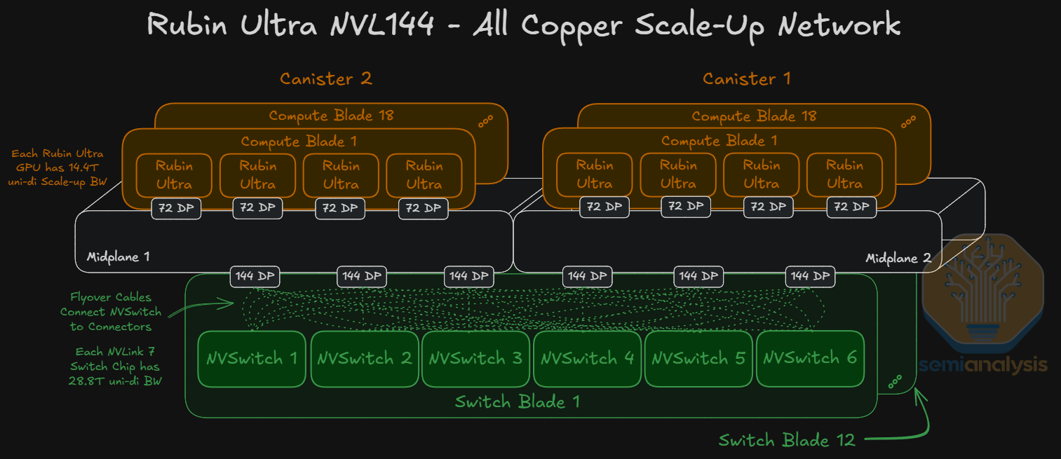
In the Kyber Switch Blade picture below, we can see that there are 2 separate PCBs carrying 3 Switches each. The switch blade should have 6 152DP connectors, 3 connectors serving each midplane board. The picture is a prototype blade using less dense connectors, which is why there are 12 connectors instead of the 6 that we expect in the production version.
Each 28.8T NVLink Switch has 144 lanes of 200G (simultaneous bi-directional) which means each Switch has 24 lanes of 200G going to each connector. Copper flyover cables are used to connect each switch to the midplane, as the distances involved are too long for PCB traces. This is also why the switches are further away from the midplane, to provide space for the routing of the flyover cables.
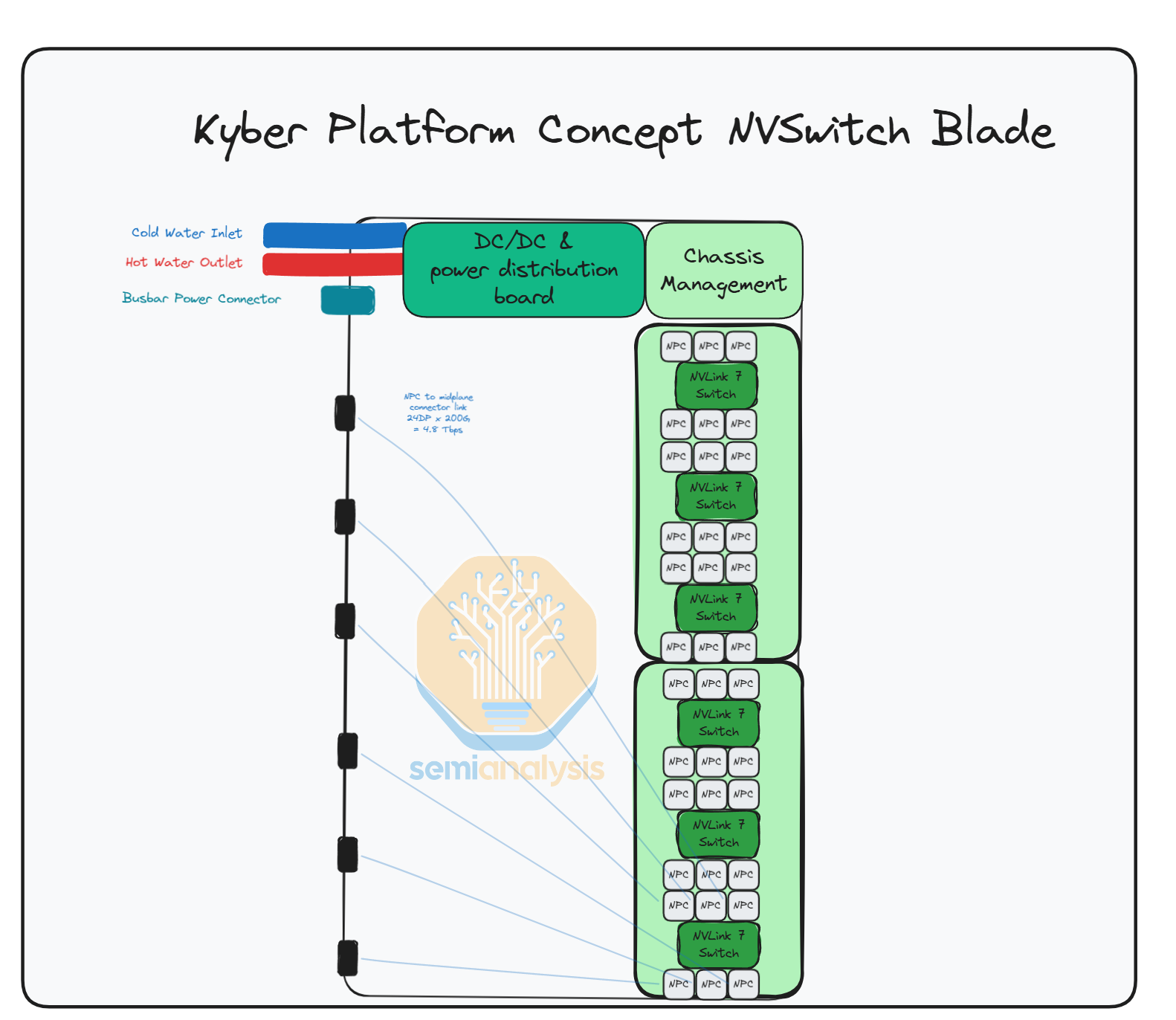
Each NVLink Switch Chip connects via flyover cables to the connector (144 DPs used x 200 Gbit/s bi-di channel = 28.8Tbit/s) connectors at the edge of the switch blade, and these connectors plug into the midplane board. Nvidia is looking into using co-packaged Copper to reduce loss further, in case NPC doesn’t work. As far as we know the Nvidia is telling supply chain to go for fully co-packaged copper.
Rubin Ultra NVL288
Though not officially discussed by Nvidia at GTC 2026, an NVL288 concept has been explored within the supply chain. This would entail two NVL144 Kyber racks placed adjacent to each other, with a rack-to-rack copper backplane used to connect the two racks. One possibility is that all 288 GPUs are connected all to all, but this would require higher radix switches than the current NVLink 7 switches which only offer a maximum radix of 144 ports of 200G.
If Rubin Ultra NVL288 is deployed, each Rubin Ultra GPU will have a scale-up bandwidth of 14.4Tbit/s uni-di, requiring 144 DPs of cables to connect the NVLink 7 switches. 72 DPs per GPU times 288 GPUs means a total of 20,736 additional DPs required to connect this larger world size domain. This entails a lot of cables, so it is an upper bound of how much cable content could be used.
The radix of the 28.8T NVLink Switch limits the number of GPUs that each switch can connect while still providing for cross-rack connectivity. Either a higher radix switch will have to be used - or there will have to be a degree of oversubscription in this architecture while potentially adopting a dragonfly-like network topology. This would also require fewer DPs worth of copper cables.
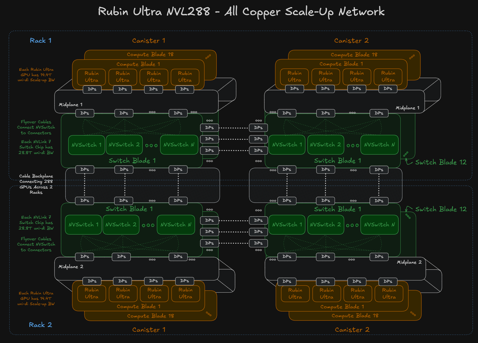
All current evidence in the supply chain points to NVSwitch 7 being the same bandwidth as NVSwitch 6, but that is seems a bit illogical to be frank. Our belief is that NVSwitch 7 is actually 2x the bandwidth and radix of NVSwitch 6, so all-to-all can be done, and architecturally that makes the most sense from a systems perspective.
Rubin Ultra NVL576
To push the scale up world size beyond 144 GPUs and across multiple racks, optics are needed as we are approaching the maximum compute density that is within the reach of copper. Rubin Ultra NVL576 is now on the roadmap with 8 racks of lower density Oberon.
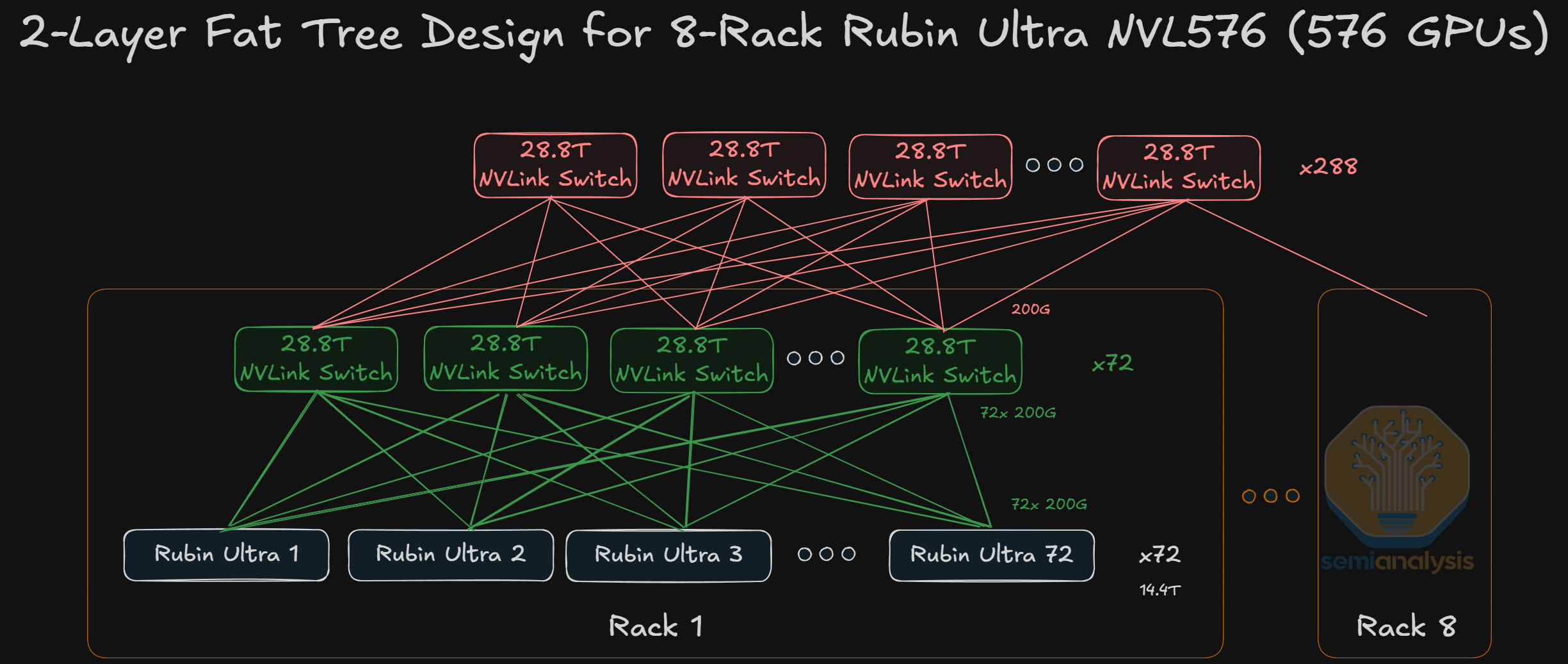
Optics will be required for the inter-rack connections, though strictly speaking it isn’t confirmed whether this will be with pluggable optics or with CPO, though CPO seems much more likely. The current Blackwell NVL576 prototype “Polyphe” uses pluggable optics.
We have shown a concept of NVL576 for GB200 previously with pluggable optics to interconnect the second layer of NVLink switches. The use of pluggables contributed to an enormous increase in BOM cost that made the system untenable from a TCO perspective for a switched all-to-all. However, it is plausible that Rubin Ultra NVL576 will be rolled out in test volumes before Feynman NVL 1,152, where we will see actual volume ramp of scale-up CPO.
The downstream implications of this are exposed in our institutional research, trusted by all major hyperscalers, semiconductor companies, and AI Labs, at sales@semianalysis.com
Feynman
While not much is known about Feynman, the Keynote sneak peek was enough to tell us Feynman will be exciting, with three major technical innovations all being pushed in a single platform: Hybrid bonding/SoIC, A16, CPO, and custom HBM.
While Feynman adopting CPO is on the roadmap, the question is to what extent? Will in-rack interconnectivity be copper based or optical? We will show possible configurations behind the Paywall. Vera ETL256
CPU demand is rising as AI workloads require more data handling, preprocessing, and orchestration beyond GPU compute. Reinforcement learning further increases demand, with CPUs running simulations, executing code, and verifying outputs in parallel. As GPUs scale faster than CPUs, larger CPU clusters are needed to keep them fully utilized, making CPUs a growing bottleneck.
The Vera standalone rack addresses this directly, achieving unprecedented density by fitting 256 CPUs into a single rack — a feat that necessitates liquid cooling. The underlying rationale mirrors the NVL rack design philosophy: pack compute tightly enough that copper interconnects can reach everything within the rack, eliminating the need for optical transceivers on the spine. The cost savings from copper more than offset the additional cooling overhead.
Each Vera ETL rack consists of 32 compute trays, 16 above and 16 below, arranged symmetrically around four 1U MGX ETL switch trays (based on Spectrum-6) in the middle. The symmetric split is deliberate: it minimizes cable length variance between compute trays and the spine, keeping all connections within copper reach. From each switch tray, rear-facing ports connect to that copper spine for intra-rack communication, while 32 front-facing OSFP cages provide optical connectivity to the rest of the POD.
Networking within the rack uses a Spectrum-X multiplane topology, distributing 200 Gb/s lanes across the four switches to achieve full all-to-all connectivity while maintaining a single network tier. With each compute tray housing 8 Vera CPUs, the result is 256 CPUs per rack, all interconnected over Ethernet through a single, flat network.
CMX and STX
We have written extensively on Nvidia’s CMX, or ICMS platform in our last Rubin piece and Memory Model. Nvidia introduced the STX reference storage rack architecture.
CMX
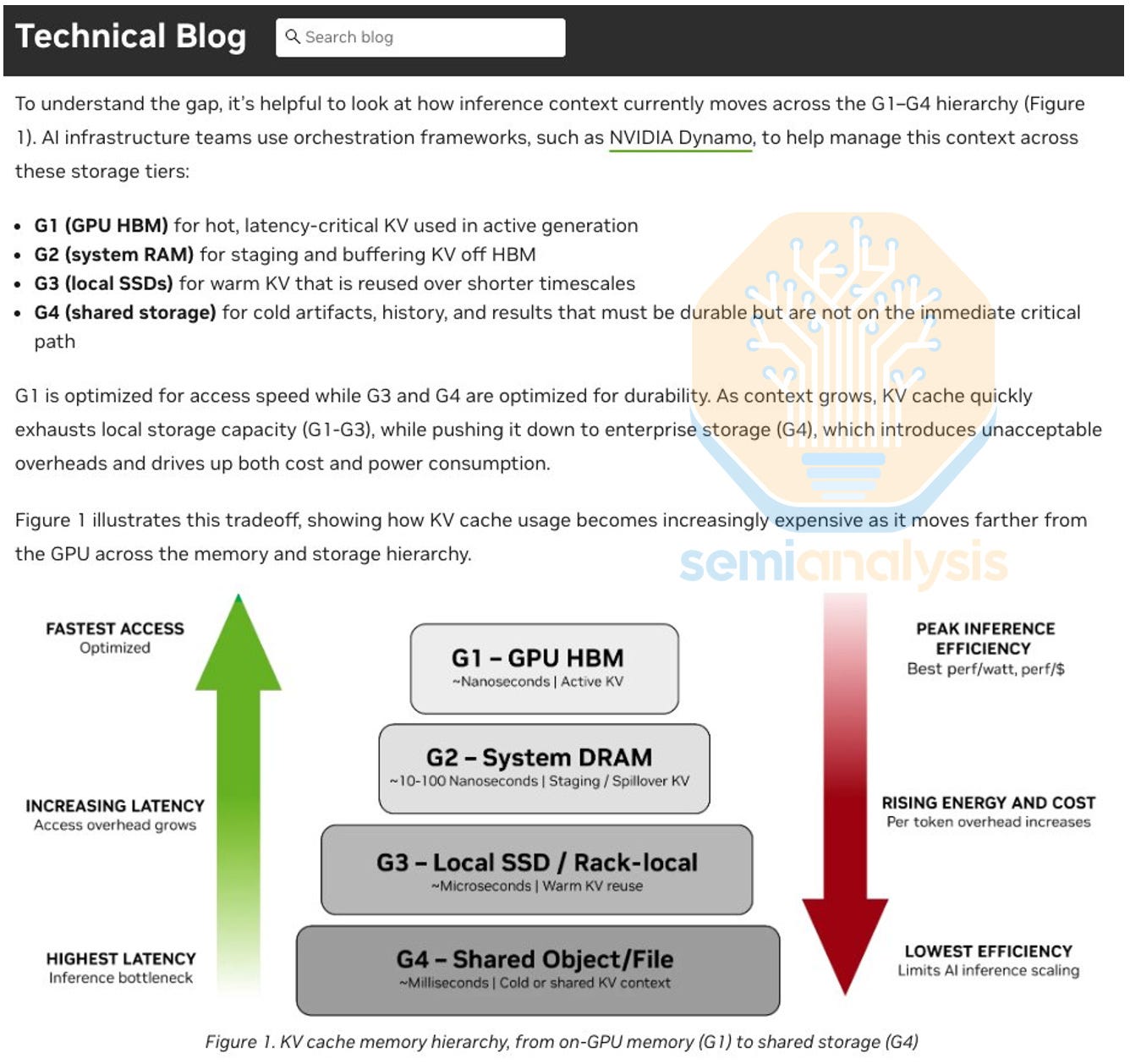
CMX is NVIDIA’s context memory storage platform. CMX addresses a growing bottleneck in modern inference infrastructure: the rapid expansion of KV Cache required to support long-context and agentic workloads.
KV cache grows linearly with input sequence length and number of users and is the primary tradeoff when it comes to prefill performance (time to first token). At scale, on-device HBM does not have enough capacity. Host DRAM extends beyond HBM capacity with an additional tier of cache, but also hits limits on total amount per node, memory bandwidth, and network bandwidth. Enter NVMe storage for additional KVcache offload.
NVIDIA introduced a “new” intermediate storage “tier G3.5” within the inference memory hierarchy at CES in January. Tier G3.5 NVMe sits in between tier G3 DRAM and tier G4 shared storage (also NVMe, or SATA/SAS SSD, or HDD). Previously referred to as ICMS (Inference Context Memory Storage) and now branded as the CMX platform, this is just another re-brand of storage servers attached to compute servers via Bluefield NICs. The only difference from NVMe architectures is the swap from Connect-X NICs to Bluefield NICs.
STX
To expand the scope of CMX, NVIDIA also launched STX. STX is a reference rack architecture using Nvidia’s BF-4 based storage solution to complement VR compute racks. The reference architecture effectively specifies exactly how many drives, Vera CPUs, BF-4 DPUs, CX-9 NICs, and Spectrum-X switches are needed for a given cluster.
Unlike the BF-4 in the VR NVL72, which consists of a Grace CPU and a single CX-9 NIC, the BF-4 in the STX reference design includes one Vera CPU, two CX-9 NICs, and two SOCAMM modules. Each STX box contains two BF-4 units, totaling two Vera CPUs, four CX-9 NICs, and four SOCAMM modules. For the whole STX rack, it has a total of 16 boxes, implying 32 Vera CPUs, 64 CX-9 NICs, and 64 SOCAMMs.
The STX announcement included a typical Nvidia show of strength where they named all major storage vendors as supporting STX, including AIC, Cloudian, DDN, Dell Technologies, Everpure, Hitachi Vantara, HPE, IBM, MinIO, NetApp, Nutanix, Supermicro, Quanta Cloud Technology (QCT), VAST Data and WEKA.
Put together, BlueField-4, CMX, and STX represent NVIDIA’s broader effort to standardize how clusters are designed at the storage layer. NVIDIA has captured the compute and network layer, and is actively moving into the storage, software, and infrastructure operations layers over time.
Now behind the paywall, we will share some more details on how all of this impacts the supply chain. Including beneficiaries of the LPX system, and the updated Kyber racks. We will also reveal a rack concept that Nvidia has yet to announce.