

The Great AI Silicon Shortage
TSMC N3 Wafer Shortages, Memory Constraints, Datacenter Bottlenecks, Supply Chain Wars Winner

The Compute Shortage
Token demand is skyrocketing and the need for AI compute continues to accelerate. The improvement in model capabilities combined with the rapid emergence of agentic workflows has driven a surge in user adoption and aggregate token demand. Anthropic added a staggering $6B of ARR in the single month of February alone driven by broad adoption of agentic coding platform Claude Code, and if Anthropic had more compute they would have added more. Despite a huge AI infrastructure buildout over the past few years, available compute is scarce. On-demand GPU prices continue to go up even for Hoppers which are almost 2 generations old.
From our own experiences, we have reached out to every neocloud we know asking if they have small clusters available, but everything is already firmly locked up. This tight supply environment explains the sharp reset in hyperscaler capex plans. Consensus estimates have moved materially higher across the board, with Google standing out as the most extreme example, where 2026 capex expectations have roughly doubled versus prior expectations, primarily driven by datacenter and server spend.

This is a tremendous level of spending, and hyperscalers would deploy even more capital if they could, but they are constrained by one critical factor: silicon supply. There is simply not enough advanced logic and memory fabrication capacity to support the pace of compute deployments. While the AD (After Da launch of ChatGPT) era has been riddled with various constraints such as CoWoS packaging and datacenter power, we are now firmly in the silicon shortage phase.

The TSMC N3 Shortage
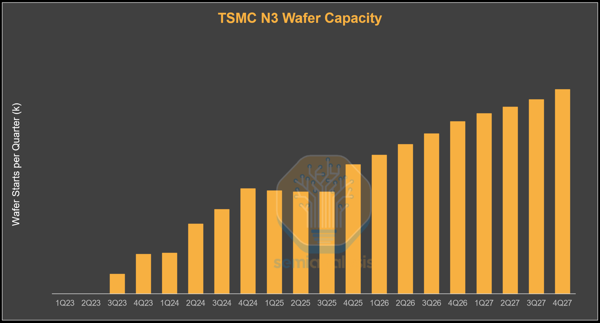
One of, if not the, biggest constraints is TSMC’s N3 logic wafer capacity. TSMC’s N3 family started shipping for revenue in 2023, with demand initially driven primarily by smartphones and PCs. N3 got off to a shaky start, with the first variant “N3B” having yield issues and being too expensive relative to the density improvement. Greater adoption came with the refined N3E process, a relaxed variant with far fewer EUV layers and therefore lower cost. Key smartphone and PC customers include Apple, which uses N3 variants for its M3 to M5 Mac chips and A17 to A19 iPhone processors, Qualcomm for its Snapdragon 8 Elite series, MediaTek for its Dimensity smartphone SoCs as well as select automotive and PC chips, and Intel for its Lunar Lake and Arrow Lake client processors.

Up until today, N3 demand has been driven primarily by consumer electronics. In 2026, all the main AI accelerator families are transitioning to N3, and AI will account for the majority of N3 demand before transitioning to N2 and beyond.
We can see in the table below the industry-wide convergence toward TSMC’s N3 family as the leading process node for AI accelerators heading into 2026. NVIDIA transitions from 4NP with Blackwell to 3NP with Rubin. AMD, typically the earlier adopter of new nodes, has already adopted N3 for MI350X and will stay on N3 for the AID and MID tiles for MI400 (XCD is N2). Google’s TPU roadmap shifts fully to N3E starting with TPU v7, with TPU seeing a huge upsize in program volumes this year. AWS also transitions to N3P with Trainium3. Meta’s MTIA follows a similar path, though it will be at much lower volumes.

This shift is not limited to XPU silicon. The Vera CPU used in VR racks uses N3P for all its silicon. There is also networking silicon in the form of the NVLink 6 switch, as well as scale out switches like Tomahawk 6 and Spectrum 6. With Rubin offering 1.6T of scale out network per GPU, Rubin kicks off the adoption of 3nm 200G optical DSPs.
This sudden convergence of N3 adoption coupled with the continued growth of AI compute demand has resulted in a huge demand shock for N3 wafer capacity. TSMC has been caught flat-footed, with wafer capacity expansion failing to keep pace with surging AI demand. How did this happen? Although the greatest compute buildout in history began in late 2022, TSMC’s capex only exceeded its previous peak in 2025. This year, TSMC is going to smash through last year’s record Capex, because they have realized how far customer demand is exceeding their capacity.

While TSMC maintains a clear technology lead over its only competitors, Intel and Samsung, that advantage matters less if customers cannot secure sufficient wafer supply to support their businesses. Capacity constraints may therefore push customers to explore greater foundry diversification. Intel, for example, has the administration’s backing and any outsourcing towards Intel Foundry will earn brownie points from the US government. Meanwhile, momentum is beginning to build at Samsung Foundry as well, with some recent design wins. First off, Samsung has secured some Tesla chip programs, such as AI5 and AI6, although they are dual-tracked with TSMC. Samsung Foundry has also entered Nvidia’s Datacenter supply chain, a development we discussed in our Foundry Model.
N3 in numbers
Now, let’s look at just how tight things are. N3 accelerator wafer demand ramps aggressively throughout this year. The primary driver is Nvidia’s Rubin production ramp as the company transitions from 4NP-based Blackwell to the N3P-based Rubin generation. However, Blackwell will still ship in higher volumes than Rubin this year given greater platform and supply chain maturity. Google and Broadcom’s TPU beat Nvidia and Amazon to N3, with TPUv7 chips already in production during 2025. This momentum continues this year with a huge increase in TPU shipment volume due to both internal Google and external demand from Anthropic and others. At the same time, the transition to next generation TPUv8 variants will begin, which will also remain on the N3 node. Another major swing factor is N3P-based Trainium3 commencing wafer-in from early 2026 for a big second half output ramp.
AI-related (accelerator, host CPU, and networking N3 demand) therefore ends up taking up just under 60% of N3 output this year. The remaining 40% is primarily for smartphone and CPU. Demand from these sources fully utilizes the entirety of N3 capacity, which gives TSMC little chance of being able to add more capacity. This tightness gets even more severe in 2027, even with TSMC adding N3 capacity. We model AI demand to be 86% of 2027 N3 wafer output nearly entirely squeezing out smartphone and CPU wafers. Part of this shift is driven by planned smartphone roadmaps transitioning to N2, but tight N3 capacity is certainly playing a part in hastening this transition. For product lines that remain on N3, demand is unlikely to be entirely fulfilled.


TSMC ultimately plays the role of kingmaker among customers competing for limited N3 allocation. In 2026, AI infrastructure customers are receiving clear priority over consumer electronics. AI accelerator designs typically have larger die sizes and more complex packaging requirements, which translate to higher ASPs. More importantly, AI-driven demand has been by far the primary driver of TSMC’s growth. End customers are willing to do whatever it takes to deploy more compute. This is backed up by multi-year visibility driven by the compute commitments of the major AI labs.
This stands in contrast to the mobile and client market that are now very much saturated, offering less opportunity for either volume or content growth. This gives AI accelerator customers a relative advantage in securing advanced-node capacity. Customers in other segments that are unable to secure sufficient N3 capacity may be forced to either extend existing product cycles or migrate directly to the N2 platform.
TSMC’s Supply Situation
With demand running far ahead of supply, TSMC is expanding capacity and pushing its existing lines to the limit, extracting every possible wafer from its nameplate capacity. As a result, effective N3 utilization is expected to exceed 100% in the second half of 2026. The company is also shifting certain process layers to other fabs to free up incremental N3 capacity wherever possible.
Why can’t TSMC simply add more N3 wafer starts? Like the memory suppliers, TSMC is constrained by available cleanroom space. Additional usable fab area must first be built before equipment can be installed and new capacity brought online. For the next 2 years, TSMC will not be able to add enough capacity to fully meet demand. As a result, for companies to get more wafer allocation in the meantime, others will have to give up their existing precious allocation, and this just may happen.
Smartphones as the Front-End Release Valve?
Smartphones are the next largest driver of N3 wafer demand this year. If anything, this is the segment most likely to see demand soften, freeing up capacity for XPU wafers. Currently, Apple and other smartphone customers such as MediaTek and Qualcomm have collectively placed supply chain orders assuming low single-digit smartphone unit growth this year.
However, rising memory prices are now flowing through to handset BOM costs and ultimately to consumer ASPs. This is likely to dampen consumer demand. We are already seeing signs that smartphone demand will be revised down to low double digit year over year declines. As smartphone demand weakens, associated wafer demand will be cut, freeing up additional capacity for XPU logic.
In terms of what this means for shipments, reallocating 5% of total smartphone N3 wafer starts in 2026 (5% of 437k wafers) to AI accelerators would enable the production of ~0.1 million additional Rubin GPUs or ~0.3 million additional TPU v7s. In a more extreme scenario where 25% of total smartphone N3 wafer starts in 2026 are reallocated to AI accelerators, TSMC could manufacture ~0.7 million additional Rubin GPUs or ~1.5 million additional TPU v7s. However, logic is only part of the equation for an AI accelerator chip, memory supply and advanced packaging is also needed.


Memory The Next Biggest Constraint
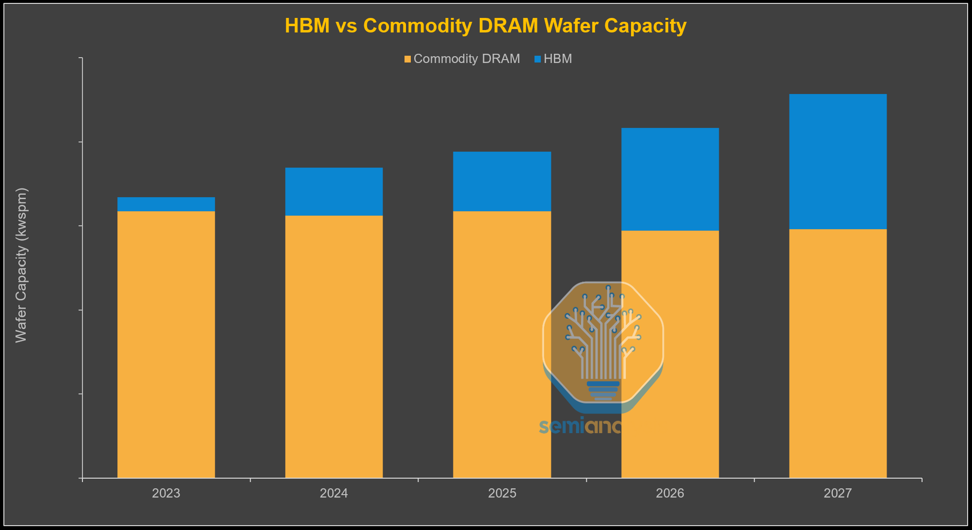
The global memory shortage is unlikely to ease in the near term. Memory has emerged as the next major battleground, as chip vendors and hyperscalers race to secure DRAM supply for accelerator production. While total DRAM wafer capacity continues to grow, most incremental capacity is being absorbed by HBM, effectively crowding out commodity DRAM.
On a wafer-per-bit basis, HBM consumes roughly three times more wafer capacity than commodity DRAM, a gap that could widen to nearly four times as the industry transitions to HBM4 this year and even larger in HBM4E next year. As a result, incremental HBM growth diverts a disproportionate share of DRAM wafer capacity away from commodity DRAM, reinforcing structurally tight memory conditions.

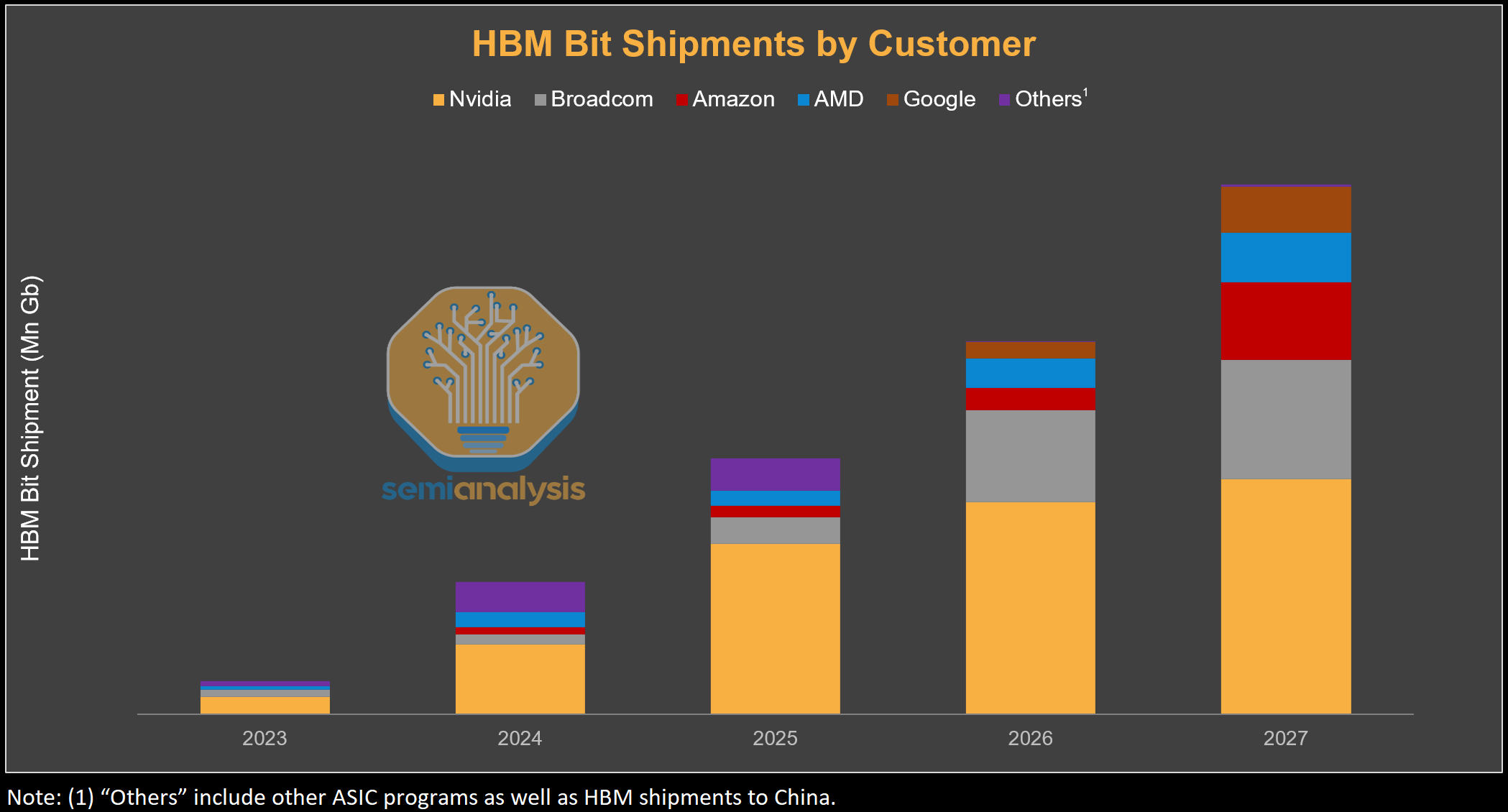
This pressure is being amplified by rapid increases in HBM content per accelerator. HBM bit shipments are inflecting sharply, driven primarily by rising memory capacity per device rather than unit growth alone. For NVIDIA, the move from Blackwell to Blackwell Ultra and Rubin increases HBM capacity by 50%, with Rubin Ultra driving a further ~4×increase. Similar step-ups are occurring across hyperscaler ASICs, with TPU v8AX and Trainium3 also migrating to 12-Hi stacks from 8-Hi in their previous generation, while AMD’s memory capacity increases by 50% from MI350 to MI400.
Another tightening dynamic is the push toward higher HBM pin speeds. Customers such as NVIDIA are targeting approximately 11 Gb/s pin speeds for HBM4, a requirement that remains difficult for memory vendors to achieve at acceptable yields. While SK Hynix and Samsung are making better progress toward meeting these specifications, Micron is lagging behind in HBM4, a dynamic we discussed in our Rubin article and within the Accelerator & HBM Model as early as January. This escalation in performance requirements, as customers demand higher pin speeds and vendors struggle to deliver at scale, further constrains effective HBM supply.

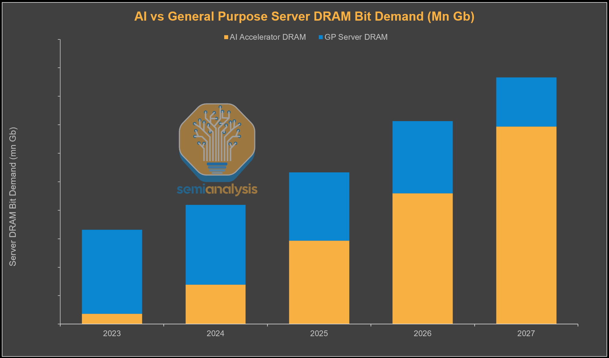
Beyond HBM, server DRAM demand is also strengthening. AI server system memory will increase materially in NVIDIA’s next-generation platforms, with VR NVL72 racks carrying 3× higher DDR content, at 1,536 GB per Vera CPU versus 512 GB per Grace. We also expect general DRAM bit demand to inflect higher in 2026, as an aging cloud and enterprise server installed base enters a multi-year replacement cycle. At the same time, AI workloads, particularly data staging, orchestration, and reinforcement learning, are driving CPU demand, gradually increasing CPU-to-GPU ratios over time.
Across the DRAM market, accelerating deployment of AI and general-purpose servers and rising DRAM content per system is expected to drive server DRAM demand higher over time. This demand should more than offset softness in smartphones, PCs, and consumer electronics over the next two years as memory prices rise.
If logic capacity is freed up for accelerators, customers will quickly need to turn their attention to securing more HBM from memory suppliers. With conventional DDR DRAM prices skyrocketing, DDR margins have surged close to or even surpassing levels at which HBM supply has been contracted. In the past, the superior margin profile offered by HBM gave memory suppliers a clear reason to expand HBM wafer capacity. However, this is no longer the case as margin dynamics have reversed, at least for 2026.
To incentivize more HBM wafer starts vs commodity wafers, customers would likely need to pay higher prices than current contracted levels to secure incremental HBM supply. This dynamic is likely to become more visible in 2027, when the next round of HBM pricing negotiations is settled. If the memory suppliers relent and shift capacity towards HBM, the available bit supply for conventional DDR DRAM would tighten even further.
Another key implication is the reallocation of bits from consumer applications to server and HBM, a dynamic we have been highlighting since 2H25. In our latest analysis in Memory Model, we highlight the impact of consumer shock on potential bit reallocation. In an extreme scenario where there is a 50% cut in consumer unit shipments, approximately 55,390 million Gb would be released, equivalent to roughly 14% of total DRAM demand in 2026. Under a 25% cut scenario, around 27,690 million Gb would be freed up, representing about 7% of total DRAM demand and nearly 80% of this year’s HBM demand.

Our base case remains a more moderate 10-15% decline in consumer shipments. Under a 10% shipment cut, approximately 11,076 million Gb would be released, representing only ~3% of total DRAM demand. In our view, this level of incremental supply is not sufficient to materially alter the overall supply-demand dynamics we expect to see this year.
The key question is how prepared memory suppliers are for consumer weakness, and to what extent they have already adjusted. We believe memory makers have a solid understanding of softness across consumer end markets. Samsung management, for example, has highlighted consumer weakness on multiple occasions, and we believe capacity allocation plans already incorporate a 10-15% downside shipment scenario. We expect other major memory suppliers to be similarly positioned.
CoWoS – Tight but Easing
Front-end capacity is now the dominant bottleneck, with CoWoS constraints easing. While CoWoS is limited, capacity planning by TSMC is with N3 constraints in mind. There is no point for TSMC to over-invest in CoWoS capacity if there is no front-end wafer supply to support it. There are also other options for 2.5D packaging. CoWoS can and has previously been outsourced to OSATs like ASE/SPIL and Amkor. For example, Nvidia went to Amkor to package H200s destined for China when the news that export licenses would be granted. Intel’s flagship EMIB 2.5D advanced packaging solution is also another option that is increasingly gaining traction, with Trainium and TPU adopting it to different degrees.
Behind the paywall, we will talk about two of the other major constraints: datacenters and power. These have shifted over time.