

Vera Rubin – Extreme Co-Design: An Evolution from Grace Blackwell Oberon
Vera, Rubin, NVLink 6 Switch, ConnectX-9, BlueField-4, Spectrum-6, Seamless Cableless Compute Tray Design, Power Rack, VR NVL72 TCO and BoM
At CES 2026, Nvidia officially announced in detail all 6 Rubin platform products: the Rubin GPU, Vera CPU, NVLink 6 Switch, ConnectX-9, BlueField-4, and Spectrum-6. VR NVL72 is the second generation of Nvidia’s rack scale Oberon architecture that takes the stage. With competition catching up on rack scale game, Trainium 3 in the Gen2 UltraServer, AMD MI450X Helios Racks, and Google’s TPU which was at rack scale even before GB200, Nvidia answers with “extreme co-design” supremacy. With extreme co-design, Nvidia takes rack scale integration to the next level. Rack system becomes a unit of compute, a single distributed accelerator, and Nvidia designs the system.
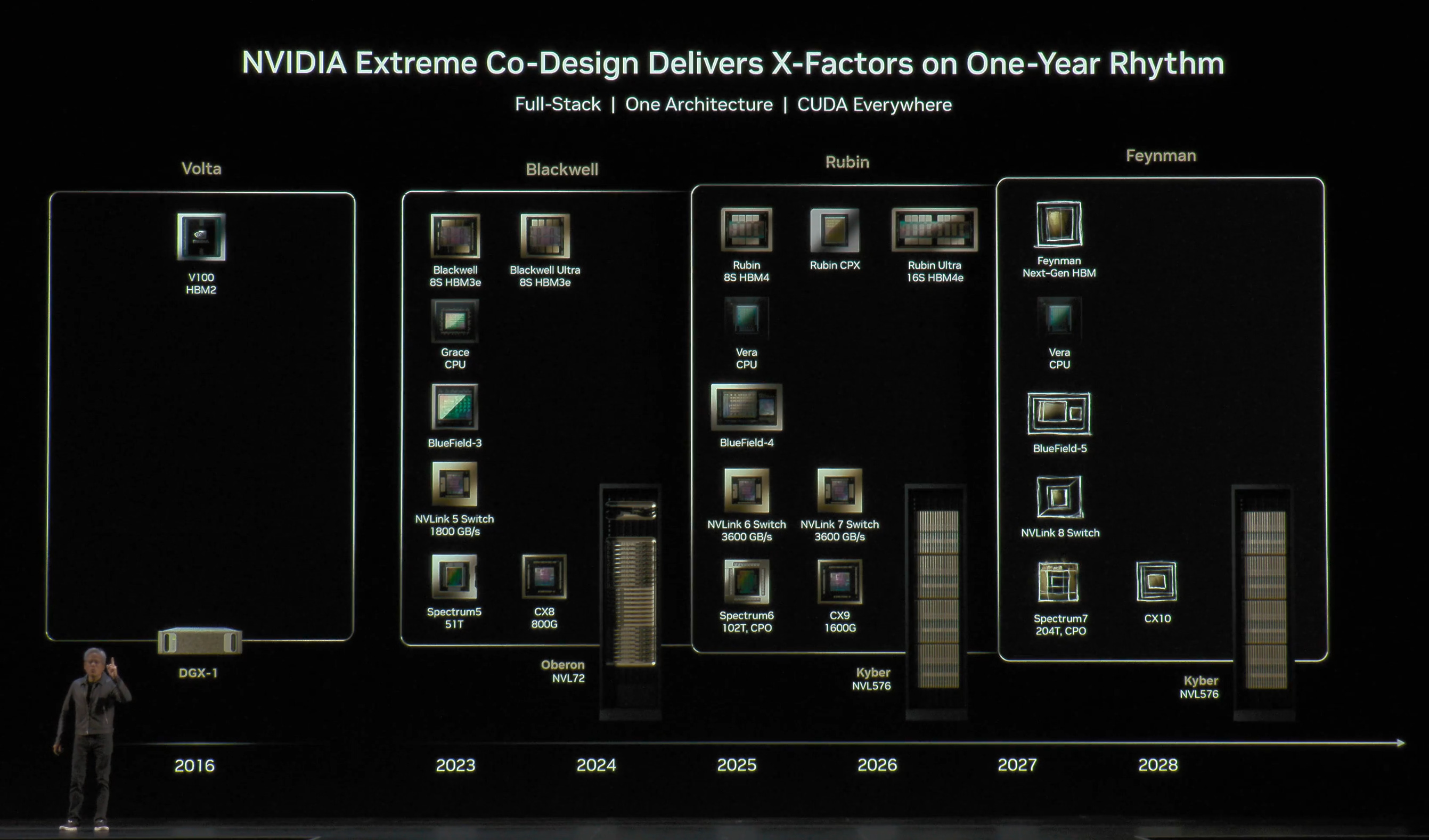
For the Vera Rubin platform, Nvidia is asserting even more control over the system and rack level design. Rack scale integration and assembly have become more challenging, as every component is being pushed to the limit, whilst also optimizing for cost efficiency. VR NVL72 has a much more holistic design with a modular approach compared to Grace Blackwell for the purpose of integration efficiency and throughput.
Nvidia’s competitiveness strengthens with its extreme co-design supremacy. It is the only player with the best in class or close to the best in class silicon product offerings for all the major silicon contents in an Nvidia trail-blazed AI server system design. Nvidia offers the best accelerator, a SOTA scale up switch, the best NIC, and one of the best Ethernet networking switch, and a much improved purpose-designed CPU. No other competitors have such a complete suite of integrated silicon products.
In the sections below, we will discuss the 6 silicon products of the Vera Rubin platform at the silicon level. Then, we will discuss the rack and compute tray evolution from Grace Blackwell to Vera Rubin from the design perspective and the implication to components: cables, connectors, PCB, thermal, mechanical, and power.
Next, we will discuss the major networks of the VR NVL72 system, namely the scale up NVLink 6 network and the backend scale out network. We will discuss the logistical implications of much more limited hyperscaler customisation and the assembly supplier landscape.
Lastly, the report ends with a discussion on the TCO of the VR NVL72 system as well as the BoM and Power Budget estimate supporting the TCO analysis. Behind the paywall, we also provide readers with insight into Nvidia’s plans for their Groq IP. We will also cover some of the challenges with regards to HBM ramp for Micron, SK Hynix, and Samsung.
Today we are also launching the VR NVL72 Component BoM and Power Budget Model. It provides a system-level bill of materials and power budget analysis for the VR NVL72 system covered in this article. This is important because various vendors and their shares of the subcomponents will drive whether they are winners or losers in the $500B Rubin buildout. The downstream impacts and dislocations in the market are large. The model covers:
Nvidia Compute Tray Content: Strata module with Rubin GPU, Vera CPU, SOCAMM memory; BlueField-4; ConnectX-9
NVLink System: NVSwitch, NVLink backplane and cabling, associated connectors, host CPU management module
Liquid Cooling Content: Coldplates, QDs, Manifolds
PCB, Substrate, and Materials Content: key system boards, ABF substrates, CCL content
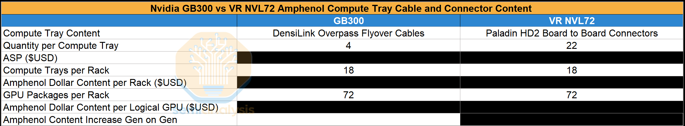
Connectors: Paladin HD2 Board to Board Connectors, Paladin HD2 NVLink 6.0 Connectors
Power Delivery Content: power shelves, busbars, VRMs, power delivery modules
Mechanical Structure: chassis, loading mechanism, railkits, rack chassis
Management modules: BMC
Networking: Transceivers, CX-9
Please visit this self service portal to purchase the model. Contact sales@semianalysis.com for any questions regarding the product.
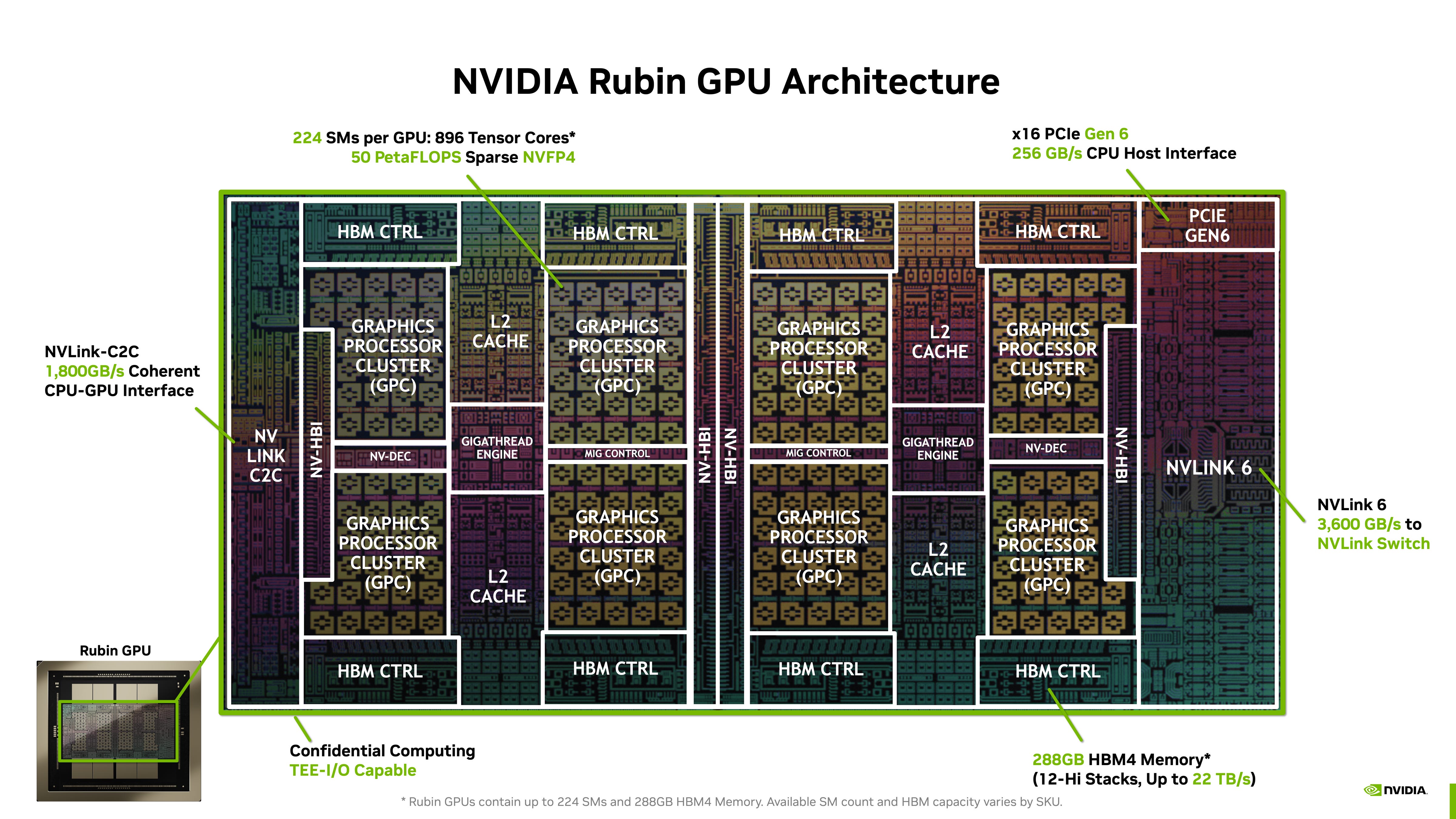
Extreme Co-design: 6 Silicon Product Offerings under the Rubin Platform - Chip Floorplans & Specifications
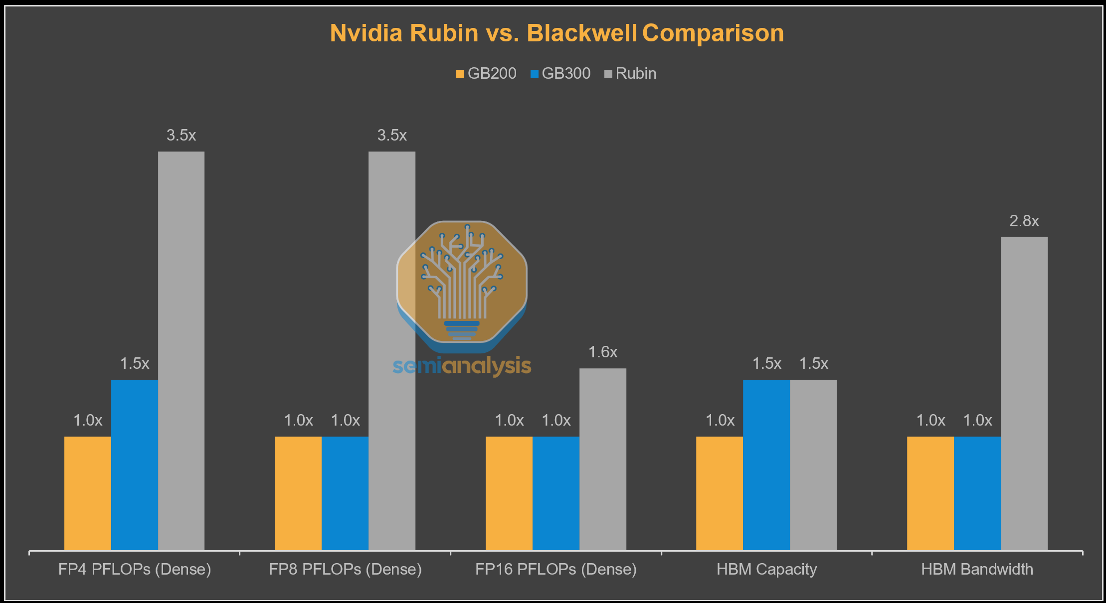
Rubin’s dense FP4 and FP8 FLOPs increase by roughly ~3.5× versus GB200, while FP16 FLOPs rise by a more modest ~1.6x, underscoring NVIDIA’s continued emphasis on FP4/FP8 as the primary scaling vector. On the memory side, HBM capacity remains flat from GB300, while HBM bandwidth scales more aggressively at ~2.8x. Overall, the architecture prioritizes bandwidth and low-precision compute.
Rubin

Rubin’s design is a logical evolution from Blackwell, with the move to a 3nm process and disaggregating I/O into chiplets while keeping the same basic structure of 2 reticle-sized dies with 8 stacks of HBM. 35 PFLOPS dense FP4 is a 3.5x improvement over Blackwell GB200, achieved by:
Increasing SM count from 160 to 224
Doubling Tensor Core width in the SM to 32768 FP4 MACs/clock
Increasing clock speed 25% from 1.90GHz to 2.38GHz
Additionally, Nvidia claims up to an effective 50 PFLOPS of FP4 performance can be achieved with an updated 3rd generation Transformer Engine that replaces 2:4 structured sparsity from prior generations. We will detail this architectural feature for Rubin below.
Notably, the Tensor core width doubling only applies to FP4 and FP8, with BF16 and TF32 remaining the same as Blackwell, resulting in performance scaling only 1.6x of Blackwell. This architectural decision reflects NVIDIA’s belief that most training and inference workloads will move away from TF32 and BF16 and onto FP8 and FP4.
On the memory front, the move to HBM4 means double the bus width per stack, running at 10.8 GT/s for 22TB/s total bandwidth or 2.75x Blackwell at the same 288GB capacity as GB300. Memory bandwidth has been upgraded significantly from the original 13TB/s advertised at GTC 2025. In order to catch up to AMD MI450’s memory bandwidth, Nvidia requested much higher HBM4 pin speeds from the DRAM suppliers - well above the speeds that was in the JEDEC specification for HBM4.
While Nvidia is targeting 22TB/s, we understand that memory suppliers are having challenges hitting Nvidia’s requirements and we see it likely that initial shipments will come in slightly below at closer to 20TB/s. We have discussed the implications to SK Hynix, Samsung, and Micron extensively for Accelerator and HBM model subscribers. Micron is well behind Samsung and Hynix and we believe they are effectively out of the picture for Rubin HBM4. We have more details on qualifications and pin speeds in the Accelerator and HBM model
The NVLink-C2C chiplet houses the SerDes for the Vera CPU connection, doubled in bandwidth to 1.8TB/s, while the larger NVLink 6 chiplet on the other end of the chip features 36 custom ‘400G’ SerDes links for 2x NVLink bandwidth to all 72 Rubin GPUs.
Transistor count has climbed 60% to 336 billion.
A notable omission from Rubin is the mention of Sparse FLOPs. In previous generations, 2:4 structured sparsity was used to double marketing FLOPs numbers. However, adoption was minimal especially at low precisions due to accuracy losses from the rigid sparsity structure forcing half of the values to be zero. Programmers basically ignored structured sparsity as it was not useful, which caused hardware designs to change as well. Blackwell Ultra GB300 added 50% more dense FP4 while keeping sparse FP4 FLOPs the same, while AMD’s MI355X stopped supporting structured sparsity on MXFP8, MXFP6 and MXFP4 formats to save silicon area.
Rubin’s adaptive compression engine in the improved Transformer Engine is a key feature to re-boost naturally sparser inference performance by doing dynamic computation of sparsity in-flight and eliminating zeros in the data stream without zeroing out non-zero values, thus maintaining model accuracy while still boosting performance. This is done automatically on existing models built for Blackwell without the need for a new programming model or specific optimizations. While models that utilize Post Training Quantization or Quantization Aware Training will be tuned to maximize adaptive compression speedups, they are not strictly needed to take advantage of dynamic compression.
This means the sparser the workload, the closer the performance will be to the 50 PFLOPS marketed peak performance. NVIDIA thus brands the 50 PFLOPS figure as FP4 Inference while the 35 PFLOPS FP4 Training number is for dense workloads. As accuracy is preserved, this allows the marketing team to claim 5x FLOPs for Rubin over GB200, comparing 50 PFLOPS dynamically compressed FP4 to 10 PFLOPS dense FP4. Whether actual GEMM performance reaches 50 PFLOPS depends on how many zeros are in the tensor. The more zeros, the closer it can reach. The less zeros in the tensor, the lower the speedup. Overall, we expect to see much greater traction for Rubin’s adaptive sparsity compression as opposed to structured sparsity thanks to the automatic implementation.
With that said, many ML Systems engineer are still skeptical that this new form of sparsity will work well, and it is very possible that Nvidia’s 50 PFLOPS is purely marketing like prior generations
Rubin’s chip level TDP increases up to 2,300W vs 1000-1400W for Blackwell. Supply chain rumors have indicated that there are 2 different “SKUs” with different power and performance profiles: a Max-P variant at 2,300W and a Max-Q variant at 1,800W. However, these are not distinct hardware SKUs but the 2 default power profiles that Nvidia is offering users based on their workload needs. Max-Q is what Nvidia believes offers the best performance per Watt. Max-P offers the greatest absolute performance though this would come with an efficiency penalty. Running the Max-P setting results in a 20% increase in rack power draw but the performance gain fall well short of this 20% power consumption increase.
These power profiles are software managed. Users can also choose whatever max power draw they prefer (as long as it is no more than 2,300W per GPU) and this has been the case for previous GPU generations as well. Several hyperscalers and labs have chosen to run their GPUs at lower power to optimize for performance per Watt as well as taking into account power availability constraints.
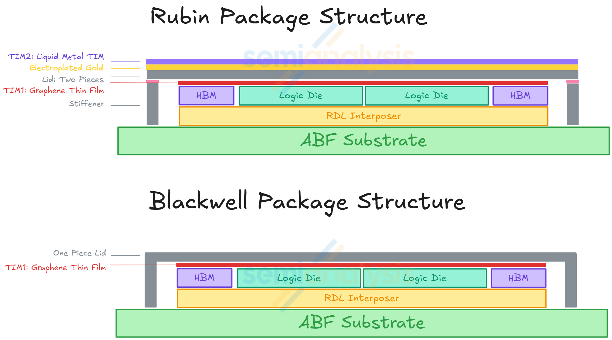
For the mechanical structure of the Rubin package, upgrades have also been made with the addition of an upgraded heat spreader and a stiffener. This compares to Blackwell B200 and B300 packages that only have a heat spreader lid. The heat spreader lid allows more equal distribution of heat exiting the package. It also provides mechanical support for the package to prevent warpage.
For Rubin, the heat spreader lid is a module made up of two separate lids. Beside the heat spreader lid, a stiffener is added to the package structure to provide even more mechanical support to avoid warpage. At the surface of the heat spreader lid, there will also be a layer of electroplated gold. The reason for this is to prevent corrosion from liquid metal TIM2, which is between the heat spreader lid and the cold plate.
Vera
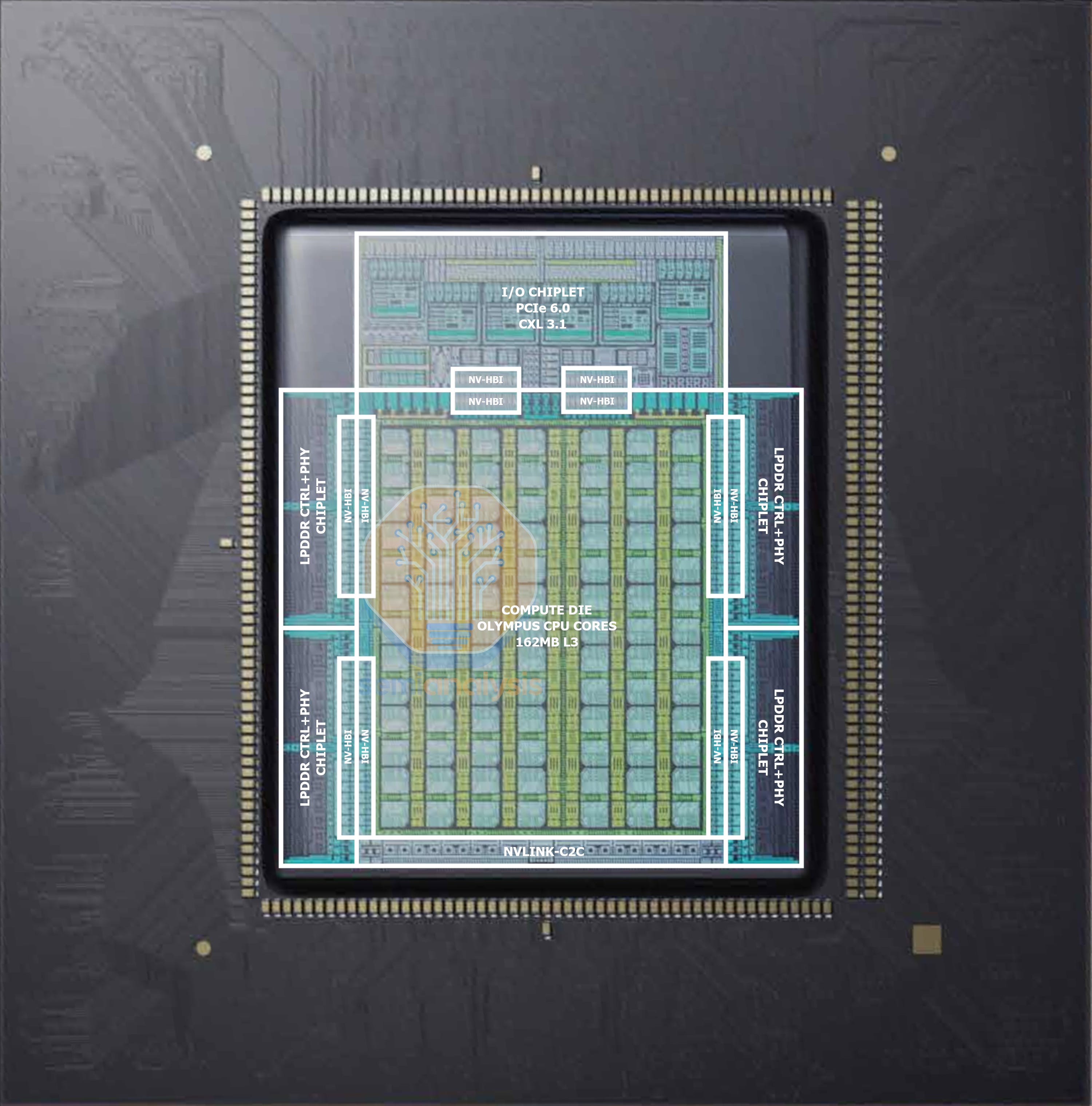
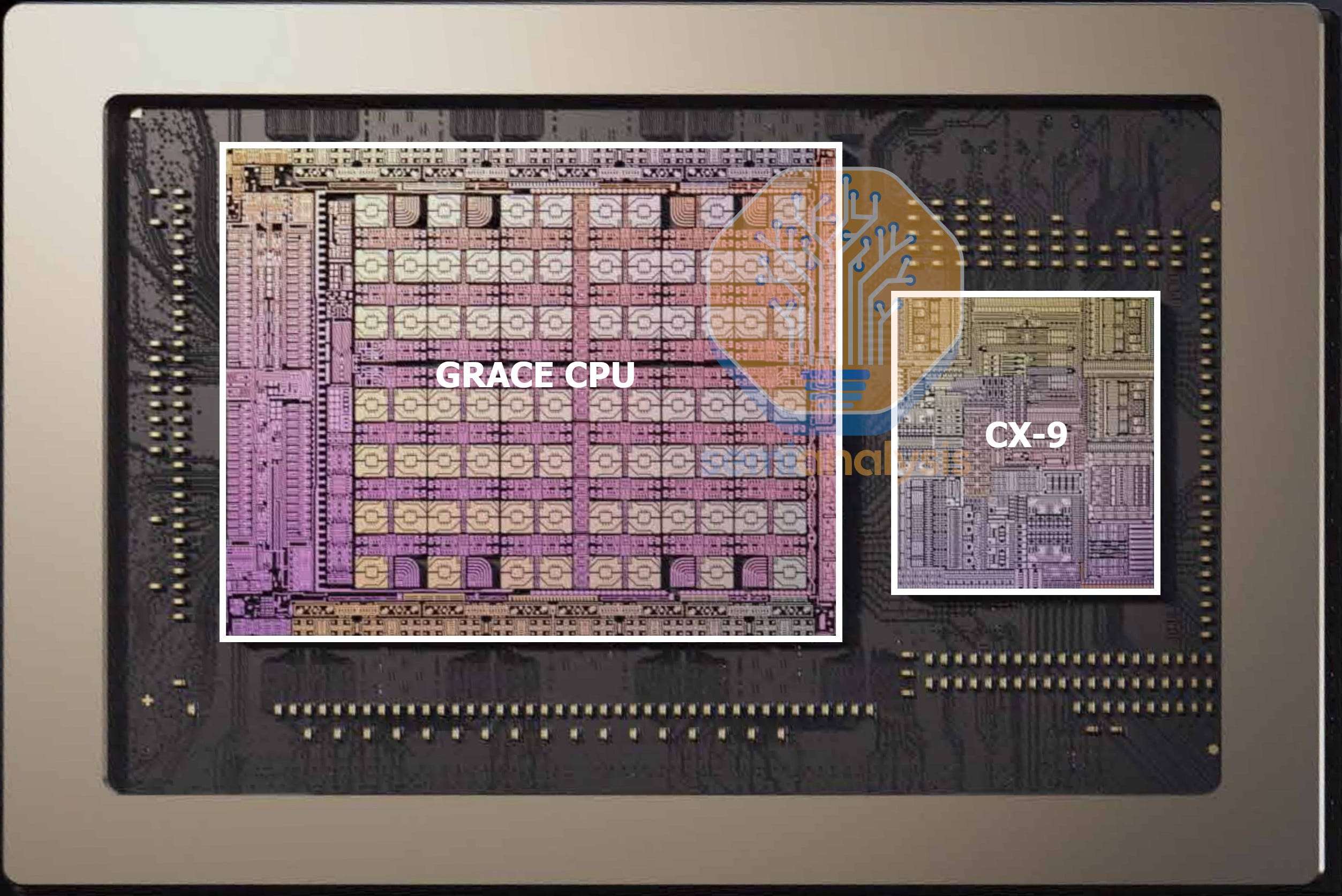
NVIDIA was aggressive on the CPU front, with Vera doubling performance over Grace by moving to a 3nm reticle-sized compute die and disaggregating the memory controllers and I/O into chiplets. Core count increases from 72 to 88, with 91 cores printed on die to leave redundancy for yield improvement. These cores mark the return of NVIDIA’s custom ARM CPU designs, with the ‘Olympus’ core now supporting SMT multi-threading for a total of 176 processing threads. L3 cache also received a 40% capacity bump to 162MB. Memory bus width doubled to 1024-bit and speed increased to 9600MT/s for 2.5x bandwidth, while maximum capacity tripled to 1.5TB with 8 SOCAMM modules. The NVLink-C2C to the Rubin GPUs also doubled in bandwidth to 1.8TB/s. PCIe6 and CXL3.1 are now supported as well. All this results in transistor count increasing 2.2x to 227 billion.
NVLink 6 Switch
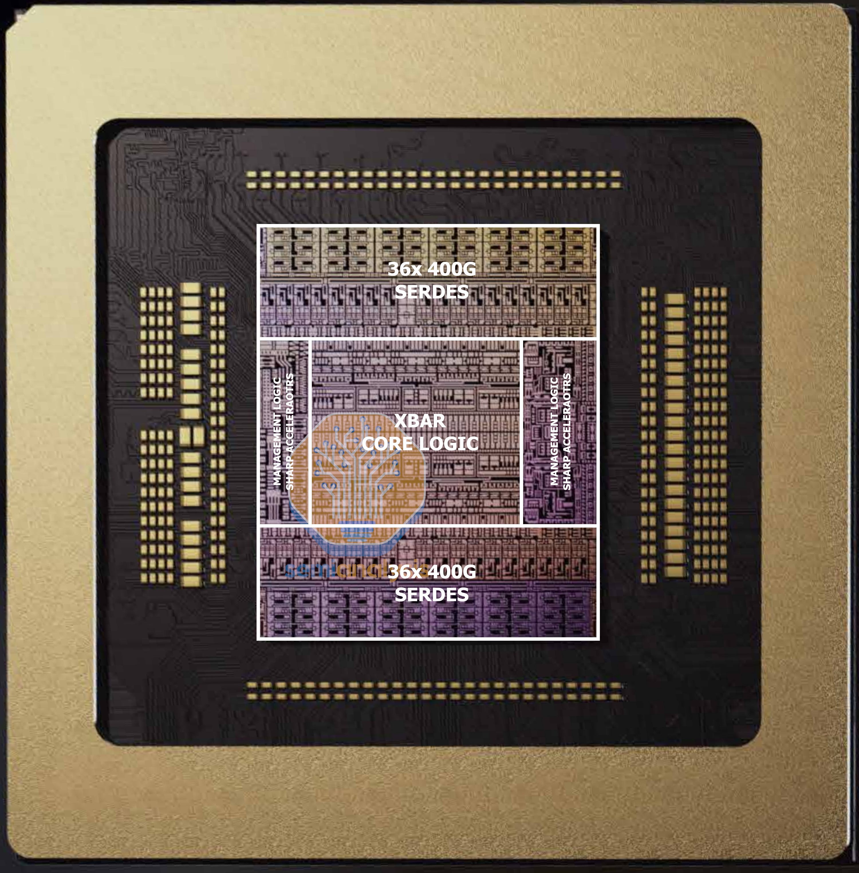
While the rack-level switching bandwidth has doubled, the number of NVLink Switch chips per rack has also doubled to 36, with each switch tray now housing 4 Switch chips. This means the new NVLink 6 Switch chip has the same 28.8T bandwidth as NVLink5 Switch, with half the number of ports but running at double the rate using ‘400G’ bi-directional SerDes. This allows the high bandwidth switch design to remain as a single monolithic die, saving on design complexity. The layout remains the same as NVIDIA’s previous switches, with 2 sides for IO and a central logic section crossbar and 3.6 TFlop SHARP in-network compute acceleration.
ConnectX-9
The ConnectX-9 is largely iterative from ConnectX-8, with the same 800G networking bandwidth and 48-lane PCIe6 switch capability. However, CX-9 now supports 800G Ethernet with 4x200G PAM4 SerDes, compared to CX-8 that only supported it on InfiniBand. For the Rubin platform, NVIDIA is doubling the number of NICs per GPU to achieve 2x scale-out bandwidth.
BlueField-4
BlueField-4’s design departs significantly from BlueField-3. Instead of doing a bespoke tapeout with compute and networking, NVIDIA simply reuses their large Grace CPU die, co-packaged with a ConnectX-9 die to make an 800G DPU with massive compute capabilities. 128GB of LPDDR5 feeds the Grace CPU at half the bandwidth of regular Grace. That is 4x the memory capacity of BlueField-3. BlueField-4 can also function as a storage controller, with four BF-4 chips in each Context Memory Storage system.
Spectrum-6
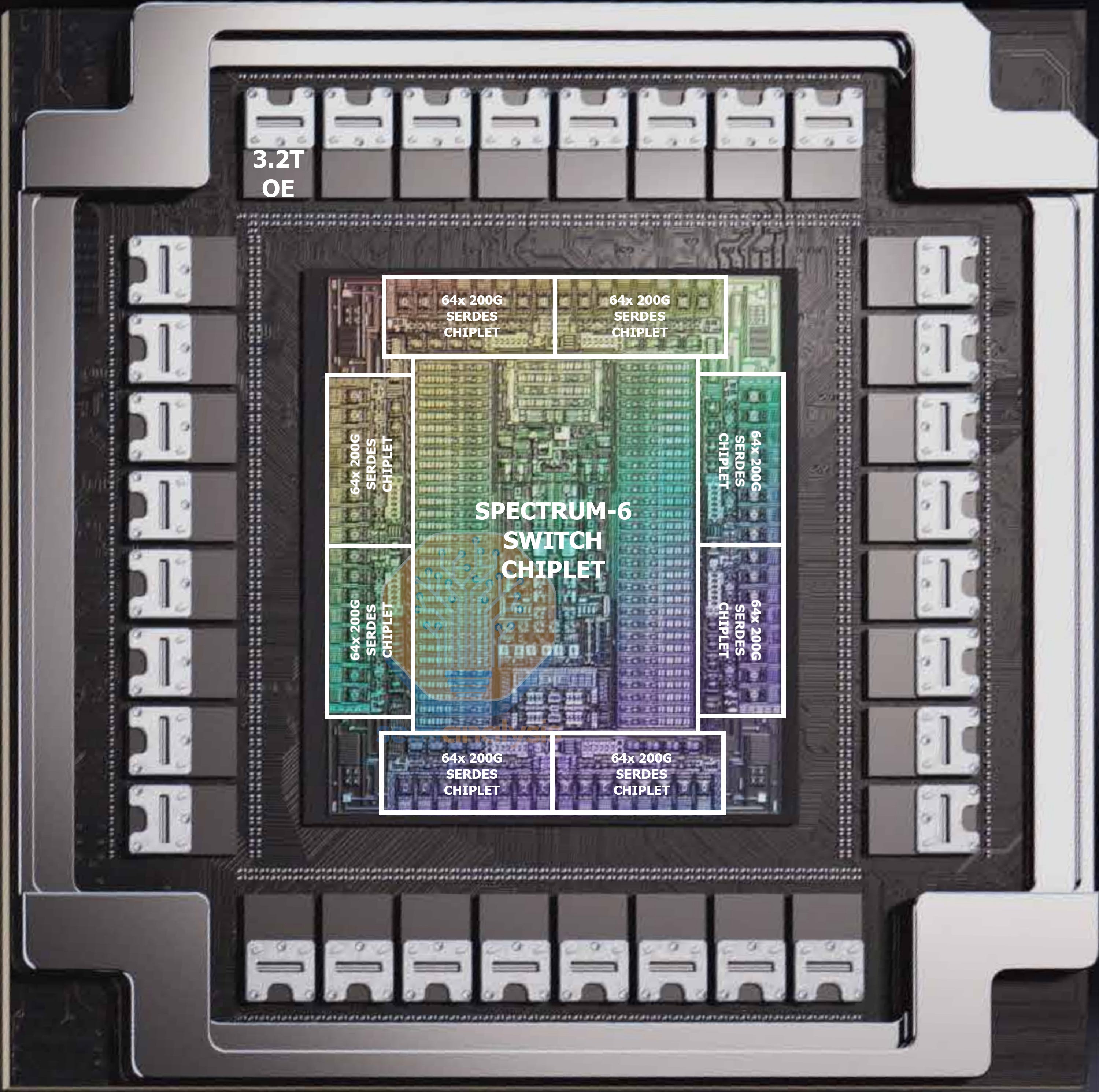
While not part of the Rubin NVL72 rack, Spectrum-6 CPO enables even larger scale-out clusters with its doubled radix. The design retains the same features as Spectrum-5, with 8 IO chiplets surrounding the main switch die. 102.4T switching bandwidth is achieved with 512x 200G SerDes. 32 3.2T optical engines on the package convert these electrical signals to optical links, each with a detachable fiber connector. The SN6810 features one of these chips, while the SN6800 houses four, multiplexed together to create a 409.6T switch box. There will also be a non-CPO version with pluggable OSFP cages in the SN6600. The non-CPO version will be more common in our view.
Rubin Oberon Rack: NVL72 not NVL144 nor NVL36
Since the announcement of GB200 at Nvidia GTC 2024, the concept of an AI server system has shifted from a chassis to a rack scale system. In our GB200 article, we discussed the evolution of Nvidia AI server form factor from HGX (8 GPU per node) to Oberon (NVL72 rack scale). While the HGX form factor still exists, the majority of Nvidia’s Blackwell GPUs are integrated in the Oberon form factor. Rubin will also be offered in both HGX and Oberon systems.
The key difference between the Blackwell and Rubin Oberon architecture is the number of SKUs offered to customers. As Blackwell Oberon was the first ever mass deployment of a rack scale solution with rack power density over 100KW for the GB200 NVL72 SKU, many datacenters did not have the infrastructure ready to support 100kw+ per rack. Nvidia offered two SKUs of Blackwell Oberon: GB200 NVL72 and GB200 NVL36x2. The latter being a lower density SKU offered for customers who did not have the infra ready to handle the thermals of a single high density rack. We discussed the difference between the two form factors in the GB200 article.
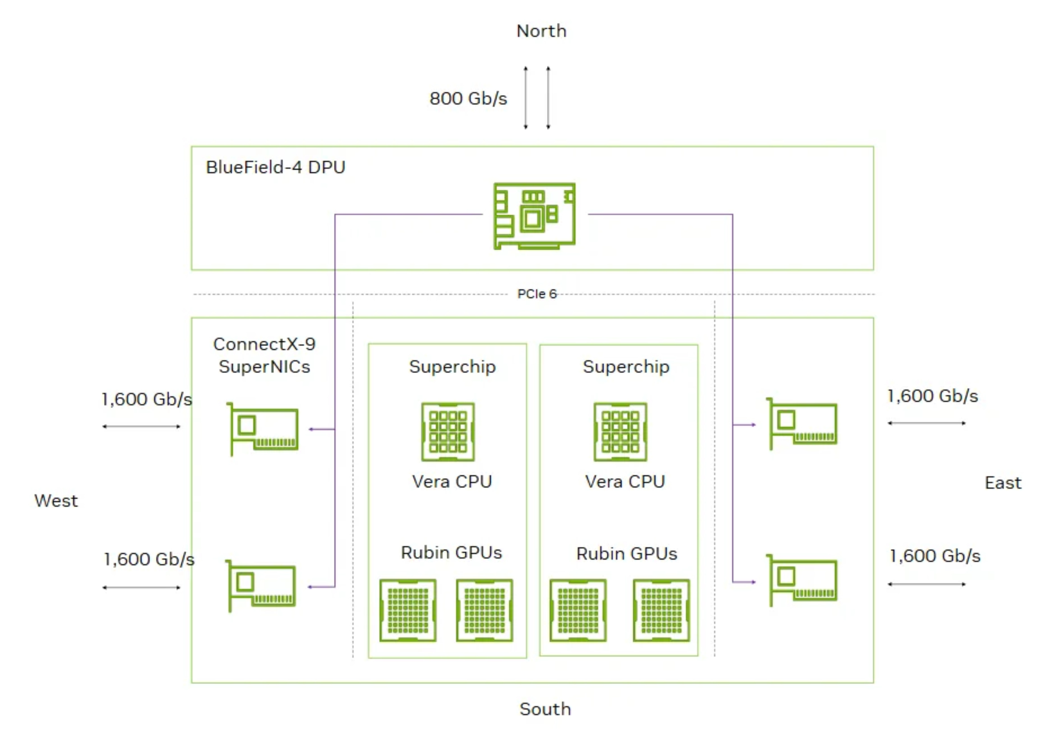
Unlike Blackwell, Rubin is only offered in the VR NVL72 SKU. The set up is very similar to that of GB200/GB300 NVL72. Each VR NVL72 system consists of:
72 Rubin GPU packages
36 Vera CPUs
36 NVLink 6 Switch ASICs
On a side note, VR NVL72 was initially known as VR NVL144 as Jensen math from GTC 2025 defined the number of GPU as the number of GPU compute die in system (with 2 compute dies per package and 72 Rubin packages per Oberon rack = 144 compute die). The naming was changed back to VR NVL72 to represent the 72 Rubin GPU packages in the system in late December. This was right before CES 2026 where the naming was officially confirmed as VR NVL72.
CPX Form Factor
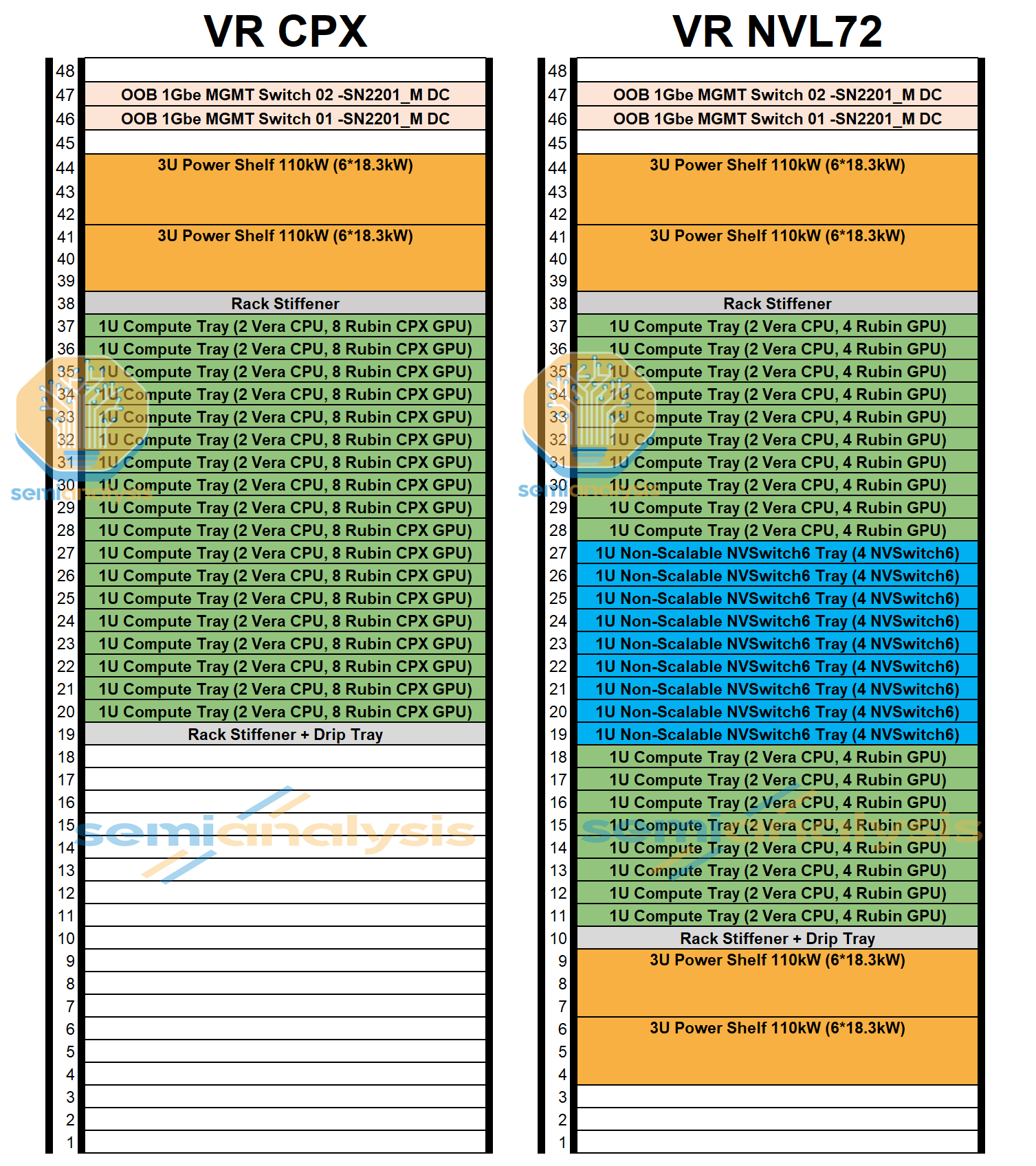
Although Nvidia initially planned to integrate the CPX accelerator into the VR NVL72 rack, the current development suggests that CPX will only be offered as a standalone rack as we detailed in our article introducing Nvidia CPX . To recap Rubin-era system planning in our previous CPX article, Nvidia initially contemplated three VR NVL72 configurations:
VR NVL72 (Regular): Standard Oberon VR NVL72 without CPX
VR NVL72 CPX (Integrated): Rubin GPU and Rubin CPX within the same compute tray
VR NVL72 CPX (Dual Rack): Rubin CPX deployed in a separate rack alongside the VR NVL72 rack
The standalone/dedicated rack direction materially changes the deployment calculus. A dual-rack approach allows hyperscalers to scale prefill and decode capacity independently, optimize datacenter power envelopes, and reduce system-level failure domains versus tightly coupled trays. More importantly, it formalizes architectural disaggregation between inference prefill (compute-bound) and decode (bandwidth-bound).
Rubin CPX was originally architected as a GDDR7-based accelerator optimized for prefill, based on three key considerations:
Prefill is primarily FLOPs-limited, not bandwidth-limited, making HBM less indispensable.
HBM’s increased bandwidth is structurally underutilized in prefill.
GDDR7 offers materially lower cost per GB and avoids the need for 2.5D packaging,
However, Nvidia began exploring HBM-equipped variants for prefill, either via modified CPX configurations or through lower memory spec (such as using HBM3E) Rubin deployments dedicated to prefill, which we noted this way back in early December last year in our Accelerator & HBM model.
We also think a lot this shift is driven by evolving memory economics. Conventional DRAM pricing has risen sharply: As DDR pricing increases, the relative premium of HBM compresses because pricing is more locked down in long term contracts, narrowing the cost gap between a GDDR-based CPX and lower-spec HBM configurations, therefore eliminating a lot of the cost benefits GDDR offers relative to performance. While memory bandwidth is not as important for pre-fill compare to decode, it is still necessary.
Compute Tray Redesign
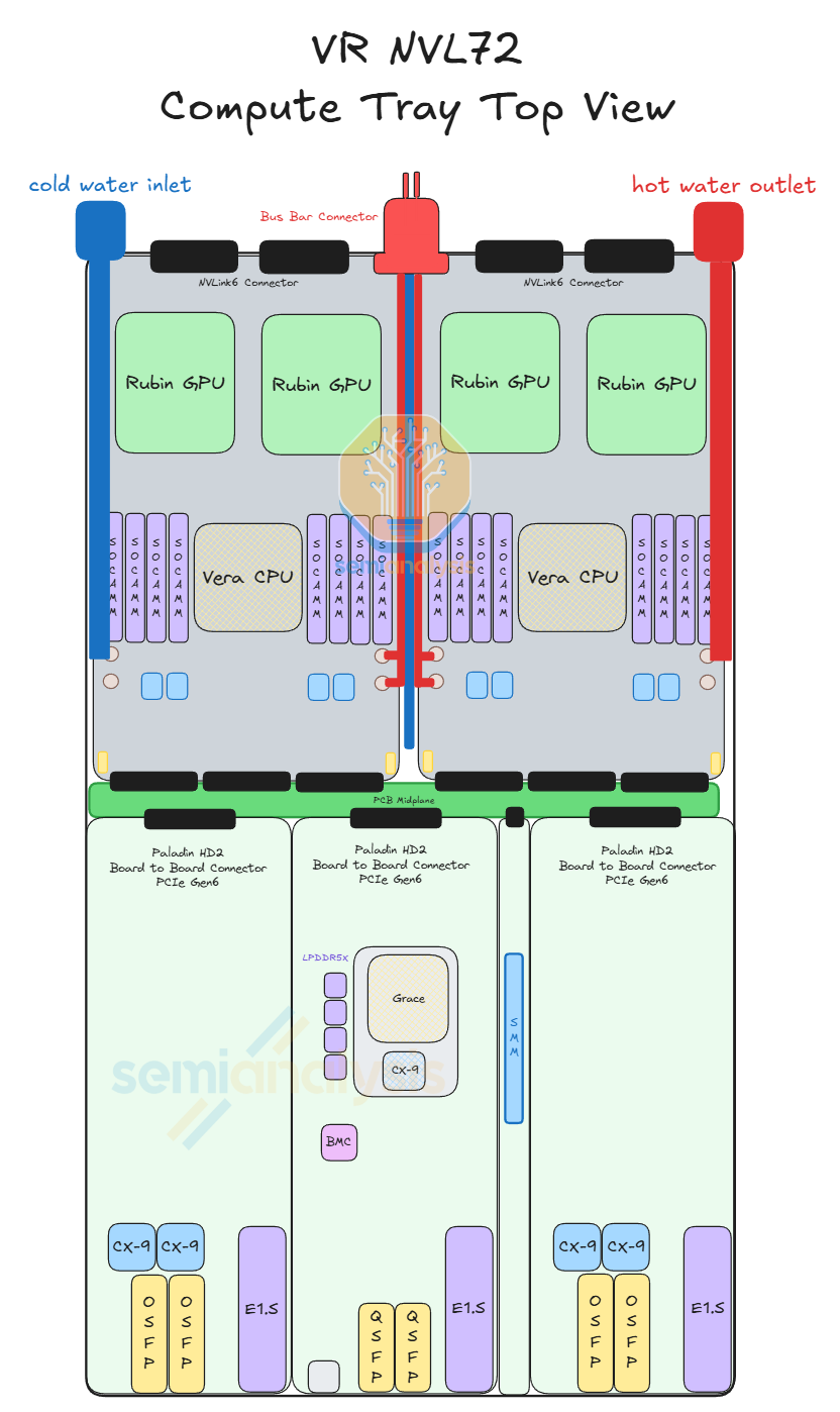
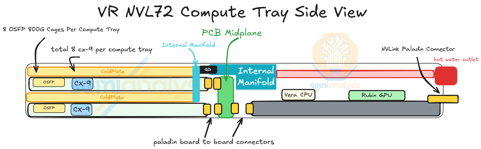
One of the major changes with VR NVL72 is within the compute tray. This redesign of the compute tray is centered around simplifying assembly, namely eliminating cables from the compute tray as cables have been the major point of failure of GB200/300 assembly. As Jensen put it at CES 2026, the cableless design reduces the compute tray assembly time from 2 hours to 5 minutes. To achieve this, the VR NVL72 compute tray adopts a modular design with the modules connecting to each via board-to-board connectors.
To understand the compute tray of VR NVL72 we must first understand the 6 modules that make up the VR NVL72 compute tray:
Strata Module x 2
Orchid Module x4
Compute Tray Midplane x 1
Power Delivery Module x 1
BlueField-4 Module x 1
System Management Module x 1
We break down these components costs and all the subcomponent costs in the Nvidia VR NVL72 BoM and Power Budget Model.
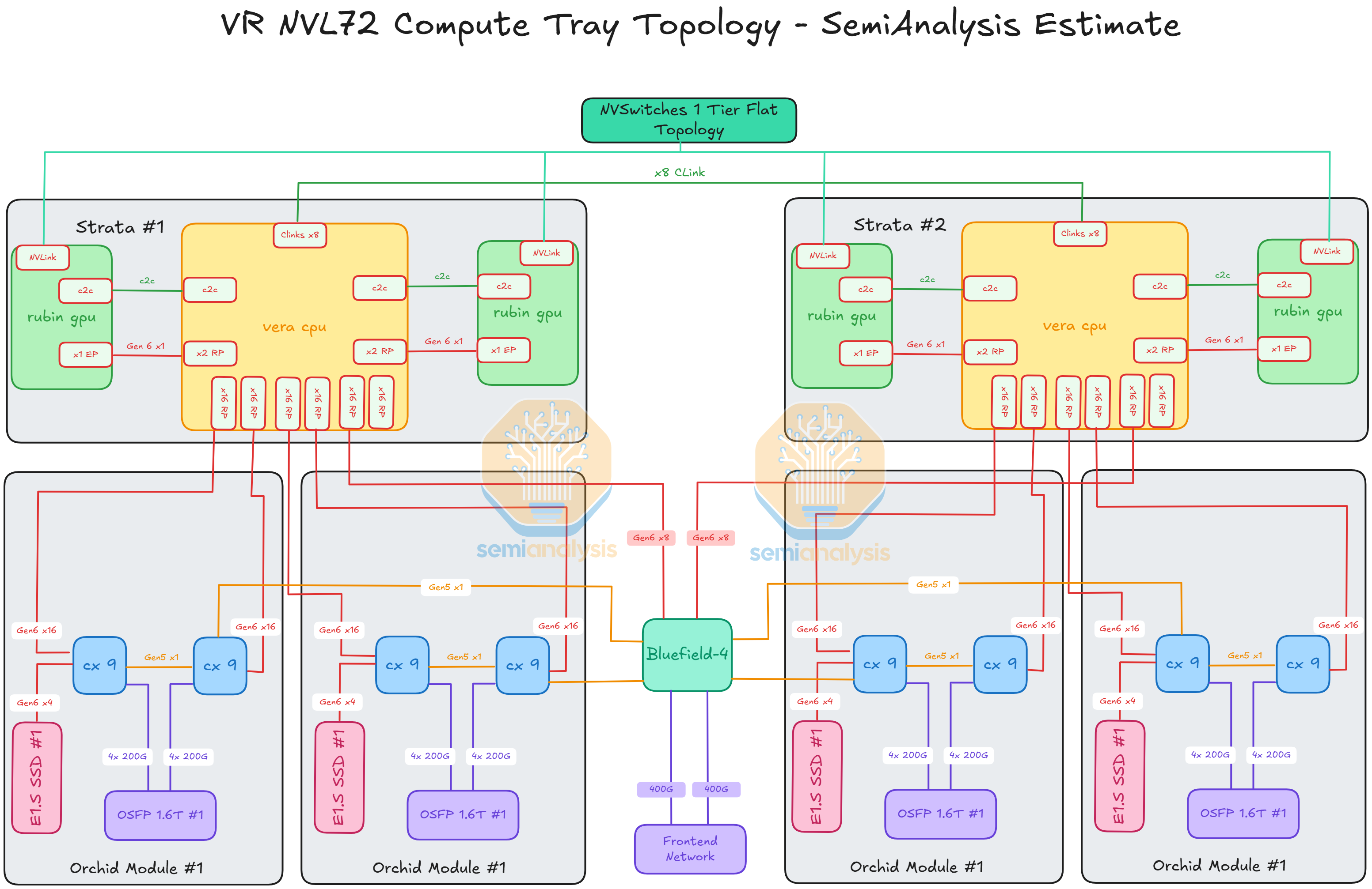
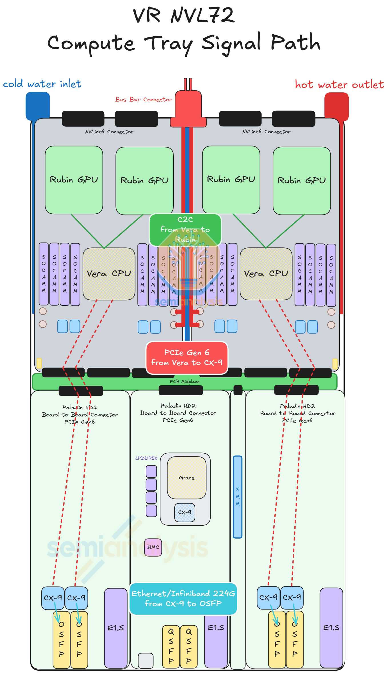
Strata
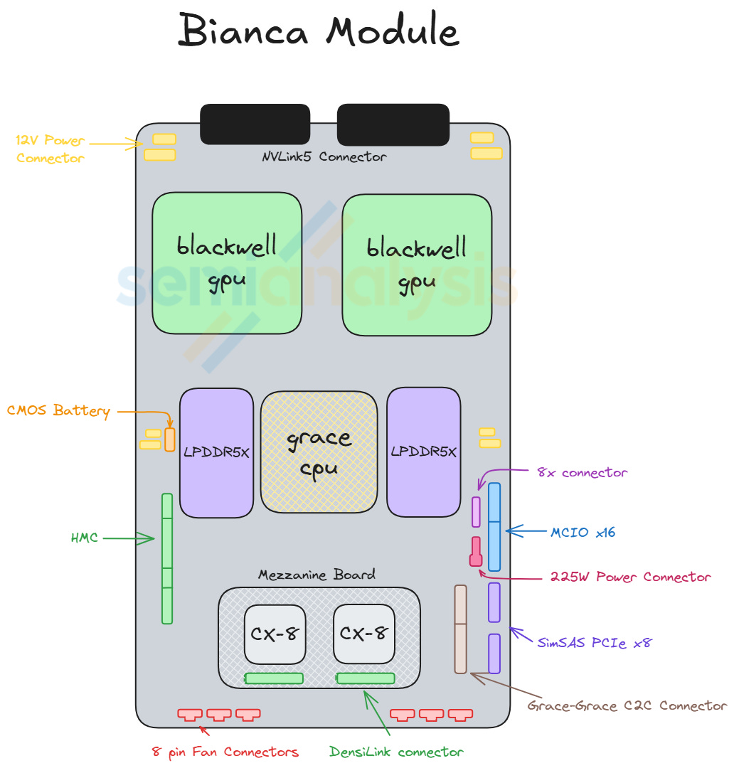
Situated at the back of the chassis, the Strata module of VR NVL72 is the equivalent of the Bianca board of GB200/300. It houses two Rubin GPUs and one Vera CPU. Unlike Bianca, the LPDDR5X memory for Vera is socketed via SOCAMM module. 8 SOCAMM sockets are placed on the left and right of Vera. Two SOCAMM modules of different capacities are offered, 192GByte and 128GByte, for a maximum of 1,534GByte and a minimum of 1,024GByte per Vera. The Connect-X NICs mezzanine module is also taken off the Strata module as CX-9 is moved to the front of the chassis. Under the cableless design, all the cable connector ports are also removed and replaced by Paladin HD2 board-to-board connectors at the bottom of the module. On the other side, the same set of Paladin HD2 backplane connectors as GB200 and GB300 are identically placed at the back of the module connecting to the NVLink 6 Switches via the NVLink backplane.
Orchid
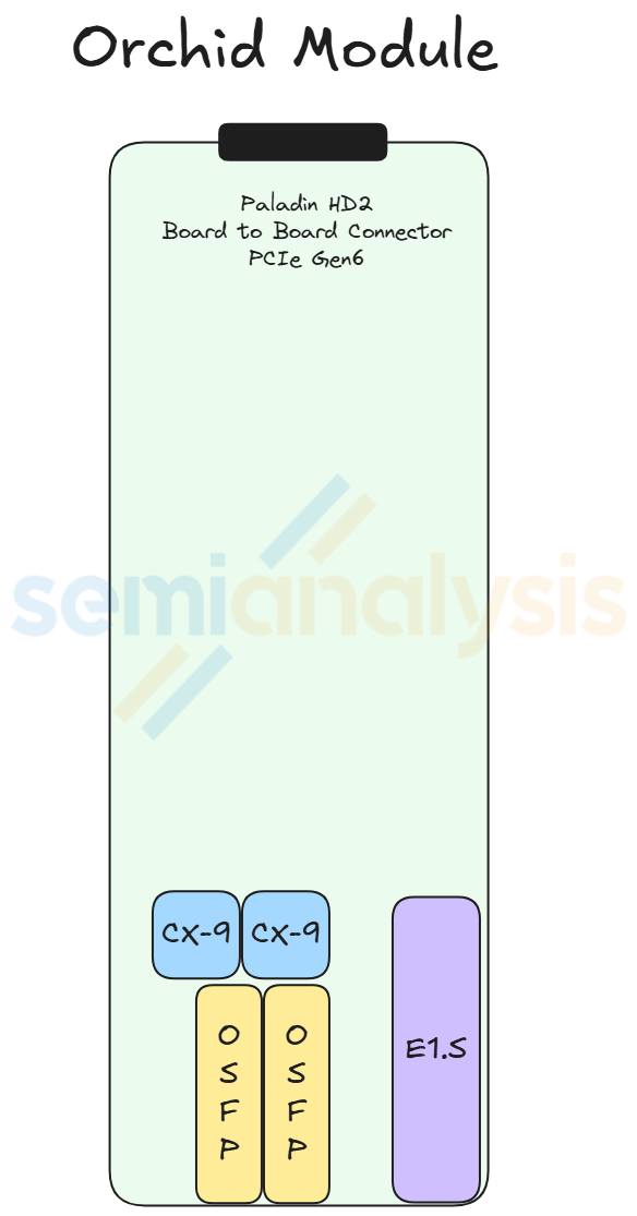
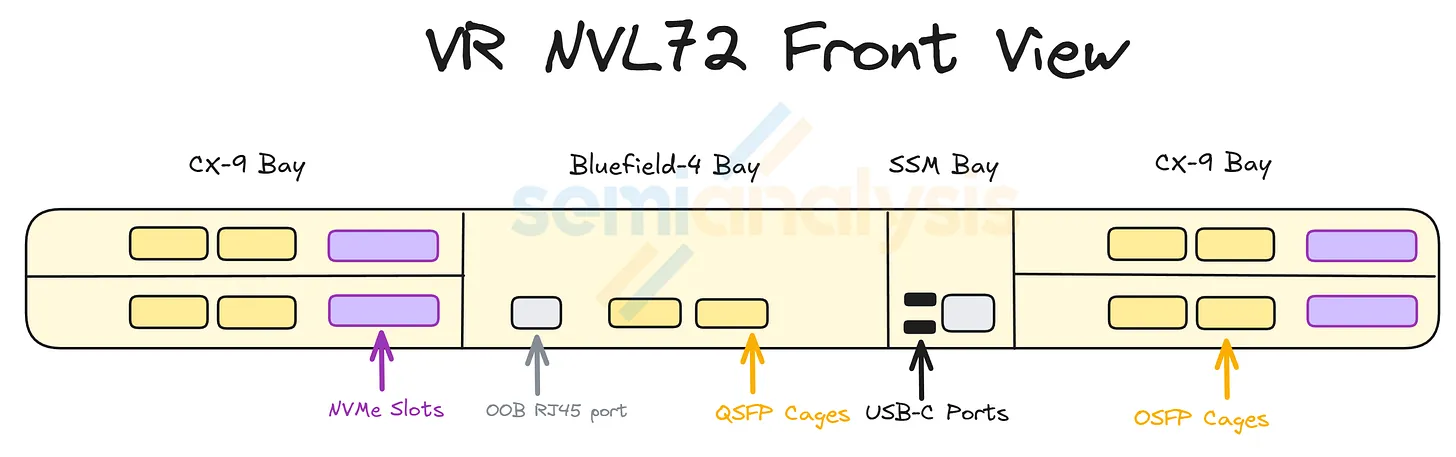
The Orchid Module houses two ConnectX-9 NICs, two 800G transceiver cages, and one E1.S module slot. Four Orchid modules sit at the front of the chassis. With two Orchid modules stacked on top of each other, they occupy the front left and front right chassis space. At the end of the module there is one Paladin HD2 board-to-board connector that mates with the connector on the midplane. The Orchid module is slim and long, allowing the PCIe 6 signal to travel from the midplane to the CX-9 NICs at the front of the chassis.
Midplane
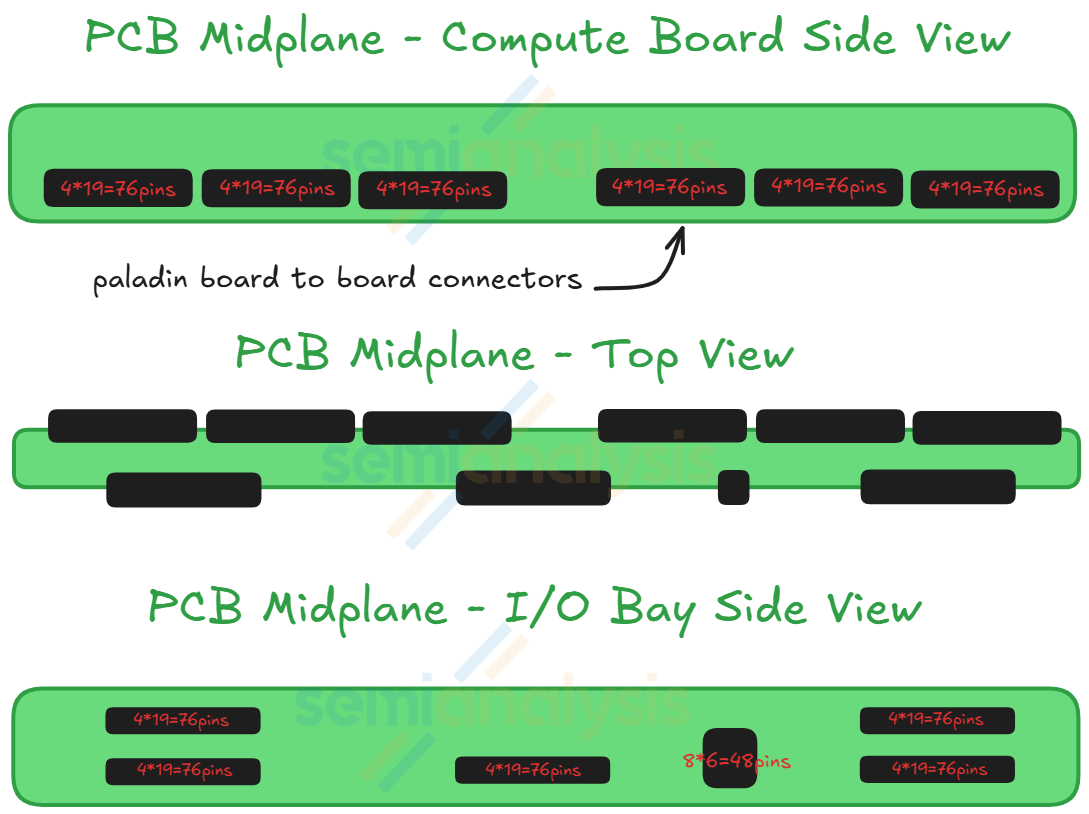
The midplane acts as a bridge for the PCIe signal between the two Strata modules and the modules at the front of the chassis. The midplane module is vertically placed across the middle of the chassis with Paladin HD2 board-to-board connector on both sides of the module. Strata modules connect to one side of the midplane while the Orchid modules, the BlueField-4 module, the PDB module, and the management modules connects to the other side.
BlueField-4
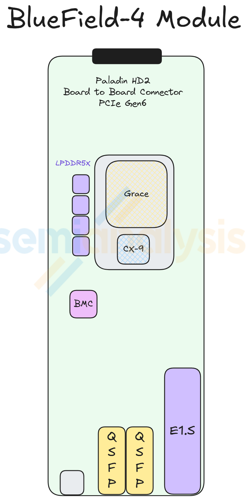
The BlueField-4 DPU sits in center of the front of the chassis between the left-side Orchid module and the management module. As mentioned in the sections above, BlueField-4 is made up of a Grace CPU and a CX-9 NIC. The module also comes with 128GByte of on board LPDDR5x, 512Gbyte of on board pluggable SSD and an integrated AST2600 BMC from Aspeed. In the reference design of the VR NVL72 compute tray, BlueField-4 acts as a DPU providing up to 800Gb/s of front end networking capability. However, just like BlueField-3, BlueField-4 will only be adopted by a handful of customers, namely CoreWeave and other smaller Neoclouds customers who have less customization capability. For most hyperscalers’ deployments, the BlueField-4 module will be replaced with their in-house frontend networking module or simply with a CX-9 which is cheaper.
Speaking of BlueField-4, it is important to discuss the new offering Jensen highlighted at CES earlier this year: ICMS, or Inference Context Memory Storage — a platform that we hear may be rebranded to “CMX” at GTC. ICMS, or CMX, introduces a third, entirely separate network dedicated solely to context memory. CMX is a purpose-built KV cache fabric. As long-context inference pushes context windows toward millions of tokens and agentic concurrency scales across users and services, the current memory hierarchy used to store KVcache begins to look insufficient.
KV cache grows linearly with sequence length and multiplicatively with workload parallelism, quickly expanding beyond what any single tier of memory was designed to hold. GPU HBM, while unmatched in bandwidth and latency, is not enough on its own to store KV especially for longer sequence length queries that are becoming popular between turns or tool calls. Host DRAM extends capacity but remains node-bound and limited in aggregate footprint and ultimately has limited capacity. Meanwhile, traditional shared storage—architected for durability rather than latency —has more access time and power overhead, making it unsuitable for participation in the decode loop.
As we noted in mid-January in our Memory Model note, Nvidia's ICMS inserts a new G3.5 tier between local SSD (G3) and shared storage (G4), optimized specifically for ephemeral, recomputable KV cache. The ICMS requires a dedicated networking layer designed exclusively for KV traffic. Wherever networking is used in this architecture, it is provisioned as a context memory network — isolated from general data movement and optimized for predictable decode latency.
The challenge with this is that the volumes of SSDs going to ICMS / CMX are quite overblown by the industry. We worked through the math in the Memory model and Tokenomics model.
BlueField-4 will be the silicon anchor of this third network. Positioned on the storage array, it terminates NVMe-oF and RDMA traffic at line rate and manages KV movement independently of host CPUs and GPUs. With 2×400G SerDes links providing 800Gb/s of bandwidth, integrated Grace CPU, and LPDDR, BlueField-4 would act as the controller for a distributed context memory fabric. In a preferred DGX-style configuration, a single BlueField-4 per tray may serve four Rubin processors, with the DPU dedicated purely to KV cache traffic and not shared with generic storage I/O.
The new CMX/ICMS ecosystem will likely include leading storage providers such as Weka, DDN, Dell Technologies, NetApp, VAST Data, and others.
Power Delivery
The power delivery module sits above the BlueField-4 module. The module receives 50V power from the internal busbar cable. Then the current is stepped down to 12V with a modular power brick. Then, 12V current is delivered to the Orchid module, the BlueField-4 module, the management modules via smaller internal busbars.
In the VR NVL72 Component BoM and Power Budget Model we have the breakdown of the power delivery content for BlueField, Strada board, and the rest of the rack’s components.
System Management
The management module is made up of multiple smaller management modules that fall under this category. These modules occupy a long slim space between the BlueField-4 module and the right-side Orchid modules. The management modules are the following:
System Management Module (SMM)
Trusted Platform Module (TPM)
Datacenter Secure Control Module (DC-SCM)
These modules provide management security functions over the compute tray. Hyperscalers usually have their own in-house management module design. Therefore, the management modules may be different for each end customer. Besides BlueField-4, the power delivery module and the management modules are the only other two components within the compute tray that Nvidia allows customization for. Some end customers are considering integrating the management modules into the power delivery module. Nevertheless, the modules need to follow the form factor that Nvidia provides so it can fit into the designated connector on the compute tray midplane.
Compute Tray Topology
The compute tray topology of VR NVL72 is roughly similar to that of GB200 and GB300. The three main differences to Grace Blackwell are the connections between GPU and ConnectX NICs, the connections to the local NVMe storage, and the connection between the BlueField-4 and ConnectX-9.
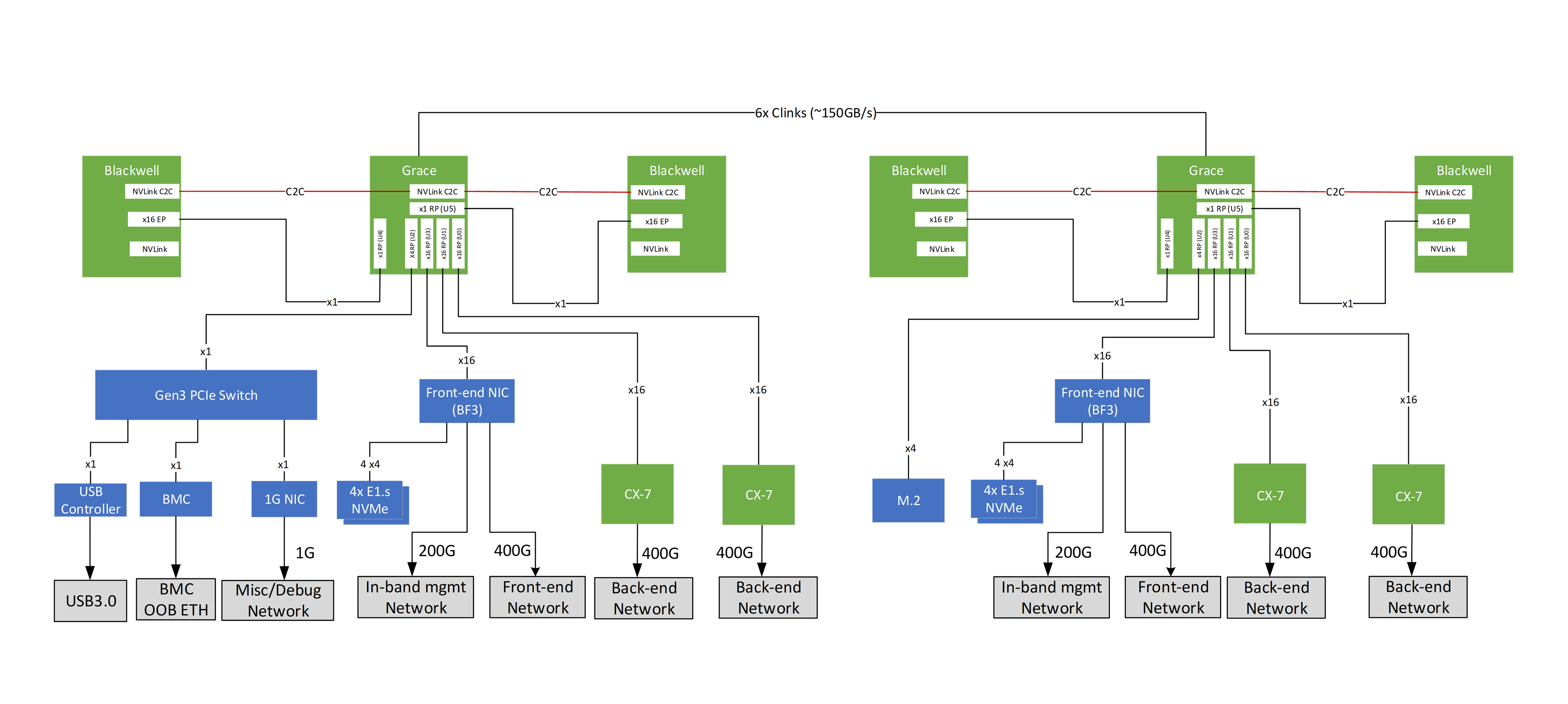
Firstly, the connection between the GPU and the ConnectX NICs evolved from GB200 to GB300 then to Vera Rubin. For GB200, the GPU does not have direct access to the ConnectX-7. Instead, B200 connects to Grace CPU via C2C connection then the Grace CPU talks to the ConnectX-7 over PCIe 5. For GB300, Nvidia introduced NIC direct to ConnectX-8, which allows the B300 GPU to communicate directly with the ConnectX-8 NIC without going through the Grace CPU.
Essentially, this means ConnectX-8 has two hosts, Grace CPU and B300 GPU. This improves latency in the backend network. However, for VR NVL72, the direct connection between Rubin GPU and ConnectX-9 is reverted back to the same design as GB200, as Rubin does not have PCIe bandwidth for two Connect-9. Rubin connects to Vera via C2C link, then Vera will connect to ConnectX-9 via PCIe6 lanes.
Secondly, the local NVMe storage for Rubin has been moved to a different location from that of NVMe storage in Grace Blackwell. Previously, local NVMe storage was managed by BlueField-3. For VR NVL72, the local NVMe storage is physically on the Orchid module managed by the ConnectX-9.
Lastly, the BlueField-4 DPU is able to control the 8 ConnectX-9 backend NICs allowing for unified management of both front end north-south network & back end high speed East-West networks. This system, known as Advanced Secure Trusted Resource Architecture (Astra), thus takes the provisioning and monitoring load off of the host CPU. The only issue with this is that BlueField-4 is expensive, so we expect most hyperscale customers to deploy their in-house DPU solutions instead. We will discuss customization more in the later sections.
Evolution from Blackwell
All of these modules in the VR NVL72 compute tray, while not exactly the same, are found in the compute tray of GB200/300. The only difference is the midplane module as it is a new component introduced to eliminate internal cables form the compute tray. Also, the modules at the front of the chassis (daughter modules) are much longer than their equivalent in Blackwell to connect the signal from the midplane to the front I/O ports via PCB. In the sections below we will discuss the cableless design, the changes in thermal design, and the changes in mechanical design in the compute tray.
Compute Tray Cableless Design
As mentioned above the VR NVL72 compute tray is designed around the cableless concept. As we discussed in our PCB Supercycle Core Research note in August last year as well as our recent Core Research note on Amphenol’s AI Content, there are two reasons for this design. First, flyover cables present multiple different points of failure as they can easily be damaged during assembly. Second, the high-density design of VR NVL72 leaves limited space for cables to be routed.
Replacing Internal Cables with Board-to-Board Connectors
For the GB200/300, the most valuable cable that is exclusively supplied by Amphenol is the DensiLink OverPass cable set within the compute tray. This cable provides the ethernet connection between the CX-7/8 NIC and the OSFP cages. However, this cable is extremely vulnerable to scratches and damage of the cable termination during assembly, thereby creating many points of failure. There are also several other lower-end PCIe cables in use (MCIO and SlimSAS) that also suffer from the same points of failure. These cables involve many other suppliers as well – complicating procurement and vendor management. Given the delicate nature of the cable, workers must be extremely careful while placing the cables in a very dense and compact chassis, which prolongs assembly time.
Although a cableless design might initially appear unfavorable for Amphenol, it is in fact a positive. Signals between the Strata module and the daughter modules still need a physical interconnect. In this architecture, those signals exit the Strata board through Amphenol’s PaladinHD2 board-to-board connectors. The signal is then routed through a PCB midplane sitting in the middle of the chassis. On the other side of the PCB midplane, the daughter modules connect to the PCB midplane via another set of Paladin HD2 B2B connectors. In our VR NVL72 Component BoM and Power Budget Model we have a detailed breakdown of Amphenol’s compute tray content in Vera Rubin NVL72. This is also discussed in more detail in our article on Amphenol’s AI Content.
Relocating ConnectX-9
To accommodate this cableless design, the CX-9 NICs, that would have been on the Strata modules, are relocated to the Orchid module (from the back half to the front half of the chassis) as illustrated in the diagram below.
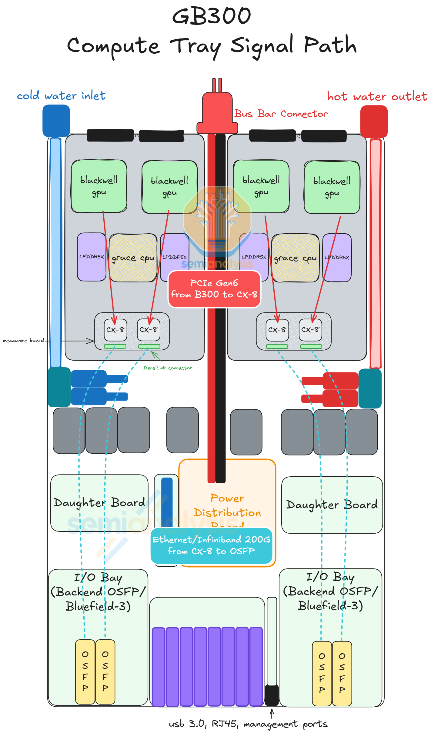
For the GB200/GB300, the PCIe signal distance between the GPU/CPU and the CX-7/8 is shorter than the Ethernet/InfiniBand signal distance between the CX-7/8 and the OSFP cages. Previously – having to transmit a 200G Ethernet/InfiniBand signal from the NIC in the back half of the compute tray to the OSFP cage in the front of the compute tray necessitated the use of flyover cables as the signal loss over PCB at 200Gbit/s (uni-directional) per lane is too high.
But now that the NIC is closer to the OSFP cage, the lower speed PCIe Gen6 signal (64Gbit/s per lane uni-directional) travels the longer distance. By making the PCIe Gen6 signal longer, the signal can travel over PCB given that PCIe Gen6 has better signal integrity than the higher speed 200G Ethernet/InfiniBand signal.
PCB vs Flyover Cables
Nevertheless, it is still challenging to drive a PCIe Gen6 signal over around 500mm of PCB distance from the Strata Module to the front of the Orchid Module. In addition to having high quality SerDes, proper signal integrity is still achievable by upgrading PCB materials.
First, we must understand why high-speed signals perform worse on PCB versus flyover cables. As SerDes rates increase, high-speed channels become increasingly constrained by insertion loss introduced by PCB traces, vias, dielectric materials and conductor roughness. Insertion loss is defined as the signal power that is lost as a signal is traveling through an interconnect channel.
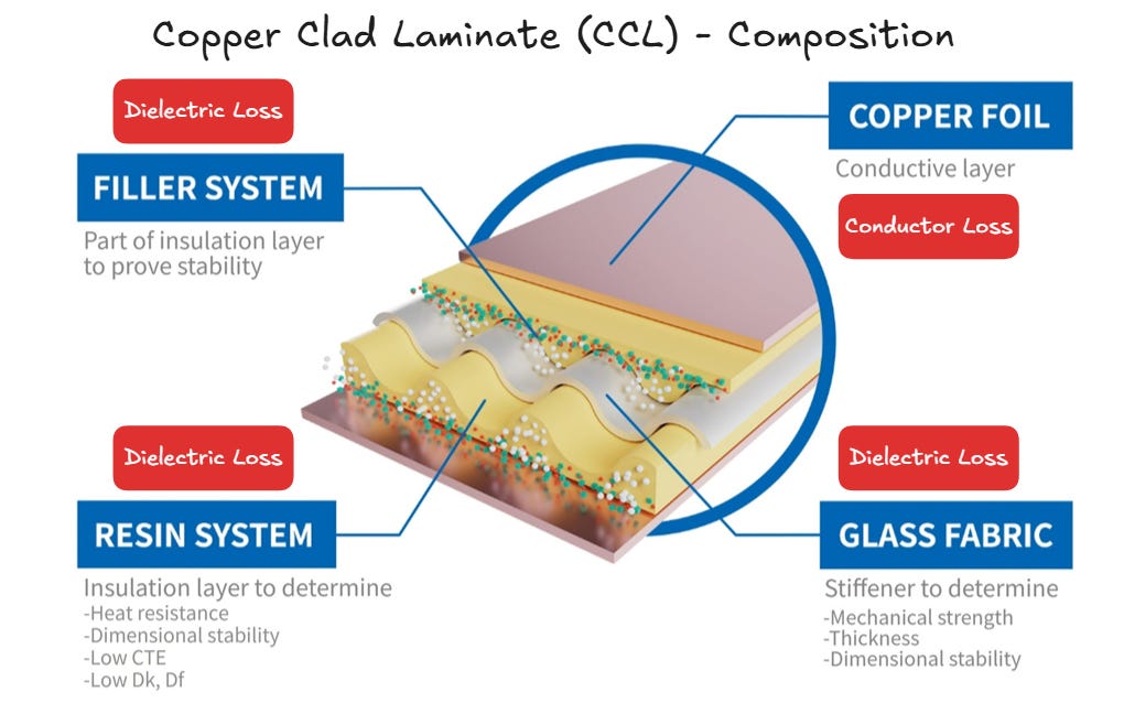
The three main mechanisms contributing to insertion loss in a PCB channel are conductor loss from skin effect and copper surface roughness, dielectric loss from laminate absorption, and geometry loss from discontinuities such as vias and layer changes.
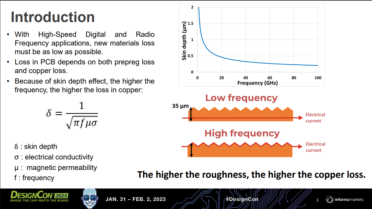
Conductor loss is driven by copper surface roughness. As signals travel down the copper traces in the PCB, energy is lost due to the resistance in copper. At higher frequencies, the signal traveling through the copper crowds toward the surface of the trace, which is known as the skin effect. On top of the natural resistance of copper, if the surface is rough, the current will not travel along a uniform path incurring more resistance and loss.
Dielectric loss is driven by the energy absorption nature of the dielectric materials. Dielectric materials, resins and glass fiber cloth, provide insulation and mechanical reinforcement function for the PCB traces. At high frequency, high-speed signal doesn’t simply travel through the copper traces, the signal traves as an electromagnetic wave with electric field extending into the dielectric materials. As the signal propagates, the dielectric absorbs a portion of the energy and dissipates as heat, contributing to insertion loss. Dielectric loss scales with frequency, hence dielectric loss is a dominant limiter of signal performance of long reach PCB traces.
Geometry loss describes the insertion loss incurred from abrupt structures of the PCB traces. Real PCB channels include many abrupt structures, such as vias and layer swaps. These are like bumps in a highway, and signals could reflect backward and be interrupted increasing insertion loss.
Another factor that affects signal performance is cross-talk. Given the increase in the number of I/Os per GPU, lane density in the PCB also increases. Cross-talk describes the scenario where the copper traces are too close to each other and the signal from one lane affects the signal in a neighboring lane. Some copper traces are designed for power as well. When the power lanes are too close to the signal lanes, noise from the power lanes can also modulate the signal as well.
In conclusion, insertion loss scales with signal frequency, and high-speed signal suffers more insertion loss from PCB than from fly over cables. Hence, as traditional CPU servers upgrade to higher signaling frequencies such as upgrading to newer PCIe generations, the CPU server design increases the adoption of fly over cables to compensate for insertion loss from the PCB. The alternative solution would be upgrading PCB materials, however, fly over cables are more cost effective and remain feasible for traditional server applications.
For VR NVL72, the design has turned toward cableless given the higher density and manufacturing complexity of AI server. The cost saved on improving higher manufacturing yields and assembly time reduction more than offsets the higher cost of the upgraded PCB materials. It is critical that all the factors that contribute towards insertion loss in the PCB are mitigated, hence PCB material upgrades are necessary for VR NVL72. We break down the cost by component here.
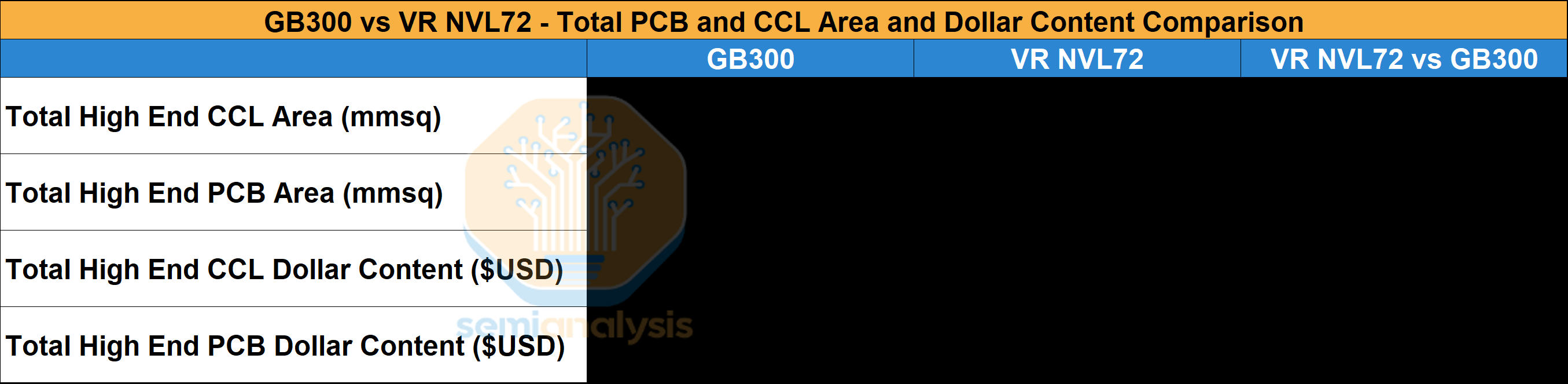
PCB Materials Upgrade and Area Growth
PCB content value in VR NVL72 will grow significantly compared to that of GB200/GB300. The two main drivers of this content growth are significant material upgrades and the notable increase of high-end PCB area and layers. Our VR NVL72 Component BoM and Power Budget Model has provides the $ content breakdown of high end CCL and PCB content for VR NVL72 vs GB200/GB300.
On the material side, CCL content upgrades from M7 to M8/M9 drives material upgrades. Copper foil is upgraded to HVLP4 across the board for the main compute and networking boards. A glass fiber cloth upgrade is necessary to reduce dielectric loss, but whether quartz cloth (Q glass) is necessary remains a debate. Below let’s discuss the materials upgrade and the key considerations behind the adoption of each material.
The Table below shows the CCL classification and PCB specification of each main board in Blackwell versus Rubin.
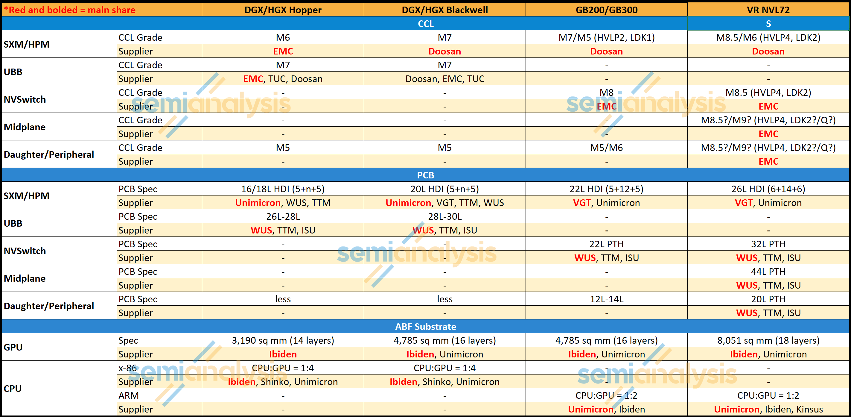
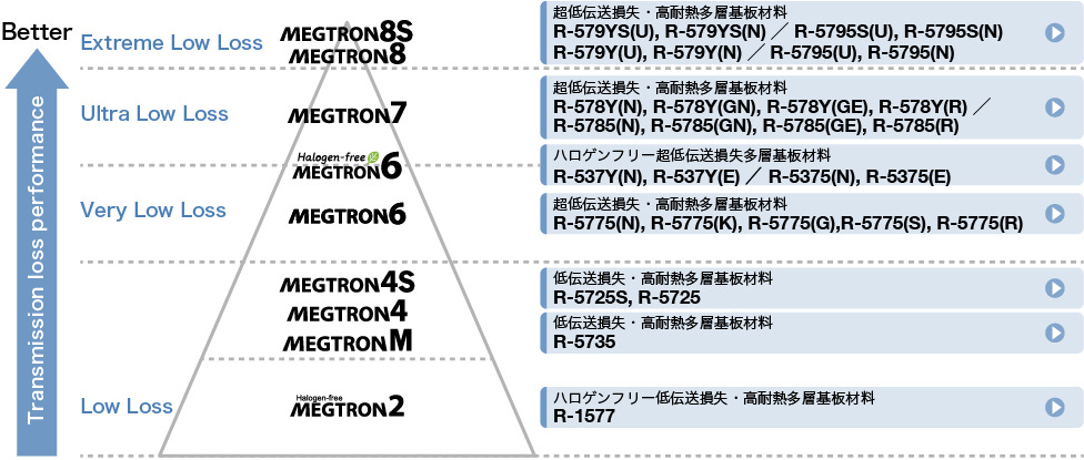
The classification of CCL materials is determined by its dielectric constant (Dk) and dissipation factor (Df) at a given frequency. Insertion loss is lower at lower Dk and Df value. The common classification is anchored to the Megtron series from Panasonic as they have been setting the industry standard. When people describe the CCL as M7 classification it usually means it matches the same Dk and Df specifications as Megtron 7 of Panasonic.
Copper foil content in Rubin is upgraded from HVLP2 to HVLP4 grade copper foil for the signal layers. As discussed earlier, due to the skin effect, smoother copper foil equals to lower insertion loss. HVLP is the classification of copper foil standing for Ultra-Low Profile Copper Foil. The higher the HVLP grade equals to lower surface roughness.
For the power layers, the additional layers in Strata compared to Blackwell are mostly power layers to accommodate more power going into the GPU. By adding more dedicated power layers, cross talk is reduced as power layers and signal layers are separated. Power layer copper foils are much thicker to insulate the current travelling through it.
The glass fiber cloth upgrade aims to reduce the dielectric constant of CCL. Beside glass fiber cloth, resin is also a key factor contributing to dielectric constant. To achieve a desirable dielectric constant, the CCL makers have their unique recipes to their formulation of the two dielectric materials in the CCL. Currently, debate around the CCL spec is around the adoption of Quartz cloth (Q glass).
Quartz cloth is the next generation material that replaces the glass fiber cloth materials as the reinforcing layer, pushing dielectric constant even lower. Besides lower dielectric constant, quartz cloth also has the benefits of being stronger, more temperature resistance, and having a lower CTE. On the other hand, the cost is multiples higher than that of the highest-grade glass fiber cloth and is much harder to process at the PCB manufacturing level, leading to worse yield.
Within VR NVL72, Quartz is initially adopted for the Orchid board and the midplane to allow the longest distance PCIe Gen 6 signal traveling through these two boards with as little insertion loss as possible. However, given the cost of the Quartz cloth and the difficulty in Q cloth processing, Nvidia is currently exploring the option of downgrading back to glass fiber cloth. The final decision is pending on the signal performance with the downgraded glass fiber cloth.
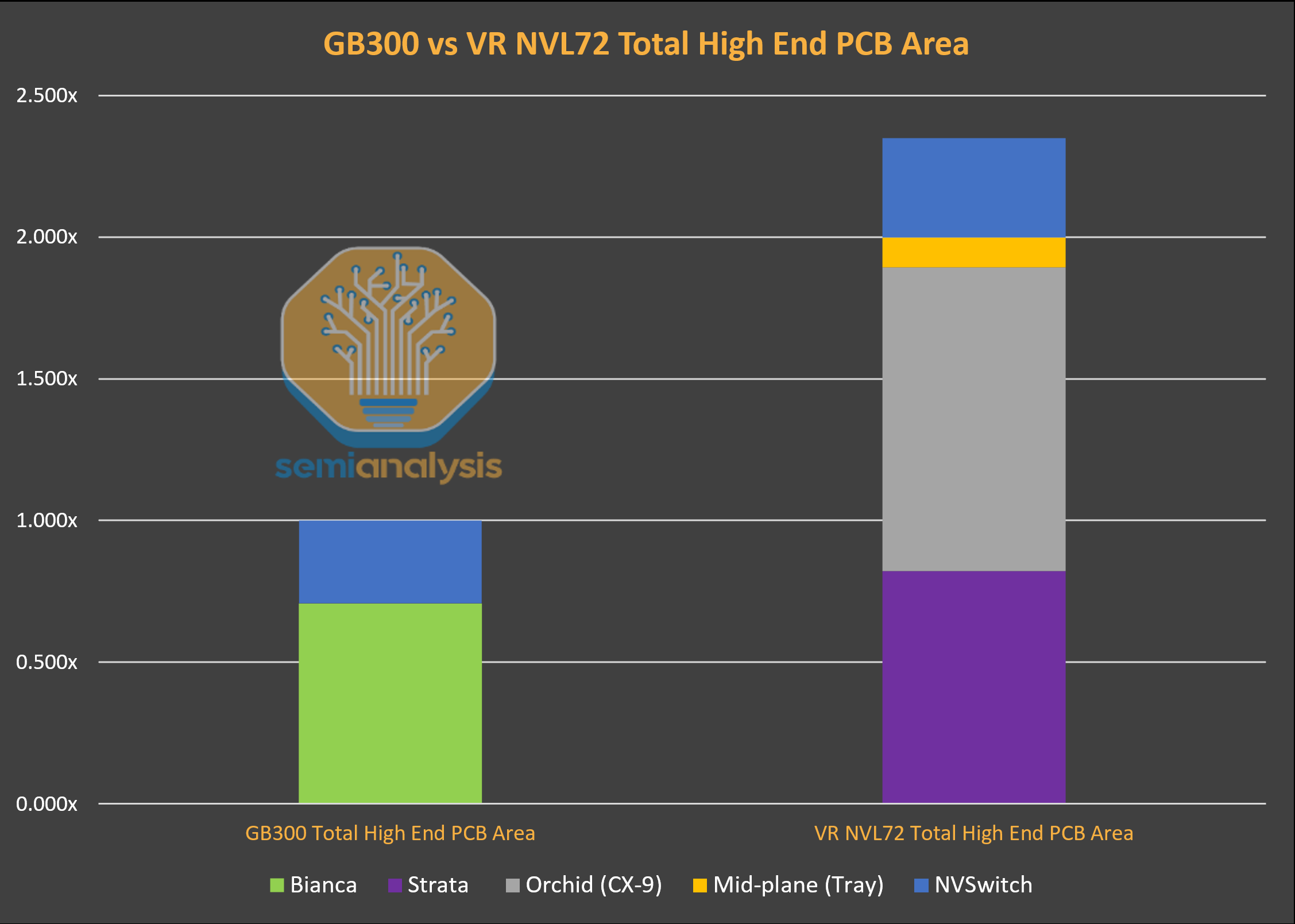
Beside material upgrade, the other driver of PCB content value is the increase of high end PCB area coverage. In Grace Blackwell, the only boards with high end material are the Bianca board with M7 grade CCL and the NVSwtich board with M8 grade CCL, leaving front half of the compute tray uncovered by high end PCB board. For VR NVL72, the Orchid board and the midplane board increases the high end PCB board area in the compute tray covering the front half of the chassis. With the Strata board bigger than the Bianca board and the extra peripheral boards in the compute tray, we estimate that the area of high end PCB board increases by ~2.3 times from GB300 to VR NVL72. As the tables shows, the Orchid board is the main contributor to the delta of total high-end PCB area between GB300 and VR NVL72 rack.
Our VR NVL72 Component BoM and Power Budget Model has provides the $ content breakdown of high end CCL and PCB content for VR NVL72 vs GB200/GB300.
Compute Tray: Thermal
VR NVL72 takes liquid cooling to the next level. The VR NVL72 compute tray is 100% liquid cooled, whereas GB200 and GB300 compute trays adopt a hybrid of 85% liquid cooling and 15% air cooling. As a result of this, fans are removed from the compute tray and the cold plate coverage increases to remove heat from the front half of the chassis. An internal manifold will be placed in the middle of the chassis to distribute inlet coolant to the various modules and to collect the outlet coolant. Each of the modules within the compute tray will have a cold plate module attached. Each cold plate module connects to the internal manifolds via MQD (a smaller form factor quick disconnect specification standard by Nvidia for compact area application within the compute tray).
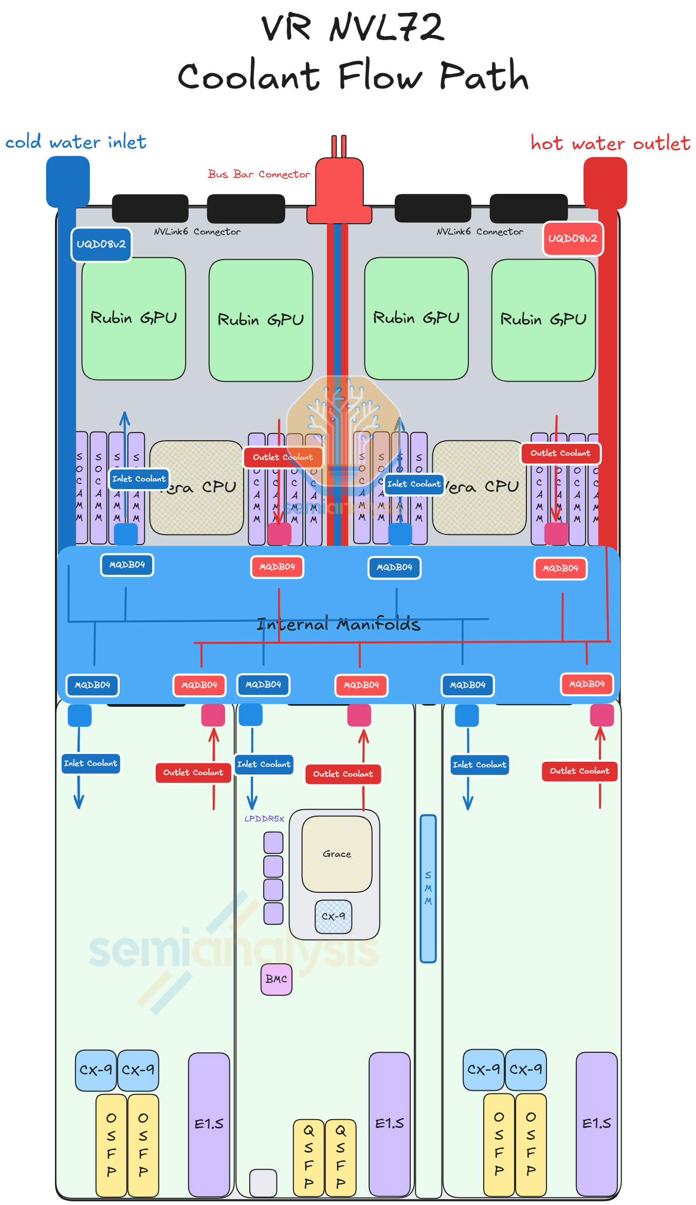
The coolant enters the compute tray via UQD from the left rear side of the chassis. Then, the coolant enters the internal manifold via a tube, where the coolant is distributed to all the modules. The coolant collects the heat from the different modules and re-enters the internal manifold. Finally, the coolant exits the compute tray via UQD at the rear right side of the chassis.
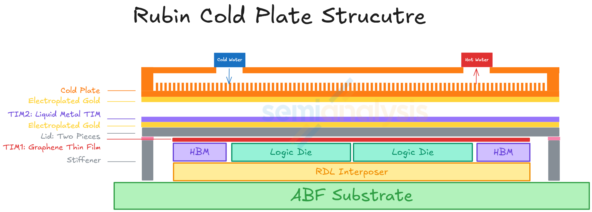
Several upgrades are also made on the cold plate for VR NVL72. For each Strata module, the cold plate will be provided as a single module covering the entire Strata board including two Rubin GPUs, one Vera CPU, SOCAMM modules, and the various VRM components. The cold plate of the Rubin GPU is upgraded to a “micro-channel cold plate” (MCCP). Essentially, the pitch between the channels in the cold plate is reduced to to 100 micron from 150 micron. This increases the surface area and increases the thermal dissipation capacity of the cold plate. Also, there will be a layer of gold plated on the surface contacting the Rubin GPU. The reason for this is to prevent corrosion of the copper from the liquid metal Indium TIM2.
Beyond the Strata module, the modules at the front of the Chassis will also have a cold plate module attached. Each Orchid module will have a cold plate module covering the CX-9, the E1.S SSD, the transceiver cages and the various VRMs. The cold plate and the board will be less than 0.5U tall as two Orchid modules are stacked on top of each other in a 1U chassis. Each pair of Orchid modules shares only a pair of QD from the manifold. There will be another set of manifolds that distribute the coolant to the top and the bottom cold plates for the pair of Orchid modules. In our VR NVL72 Component BoM and Power Budget Model we have the content for all the various thermal components including the cold plate modules, manifolds, and the Quick Disconnects.
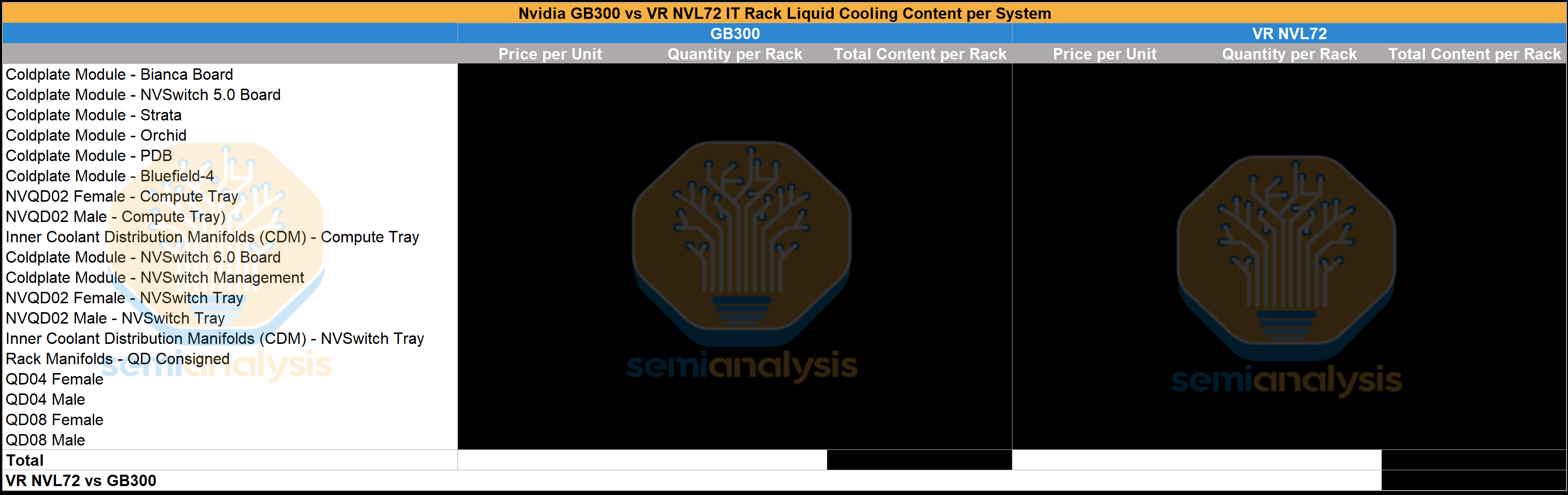
Previously, cold plates were assembled at the L10 assembly level where the various components are put into place in the chassis. Given the modular approach, the cold plates need to be more tightly integrated with the module itself. Hence, the cold plate will be attached at the L6 assembly level right after the PCBA process. This increases the assembly efficiency as the assembly at L10 is simplified to slotting in the completed modules into the corresponding connectors and quick disconnects.
Compute Tray: Power Delivery
At the compute tray level, 50VDC power enters the compute tray via the busbar clips at the back of the chassis. Then power travels to the middle of the chassis via the internal busbar cables. From the internal busbar cables, the power path is split into three destinations. The first and second path goes to the left and the right Strata Board, where the internal busbar cable feeds 50VDC power to the Strata Board directly. The third path goes to the power distribution module at the front of the chassis. The internal busbar cables will feed 50VDC power to a busbar device that travels under the PCB midplane to connect to the power distribution board (PDB) on the other side of the PCB midplane. This differs from Grace Blackwell, where 50VDC power goes directly to the PDB. Then, the PDB feeds 12VDC to all the boards in the compute tray.
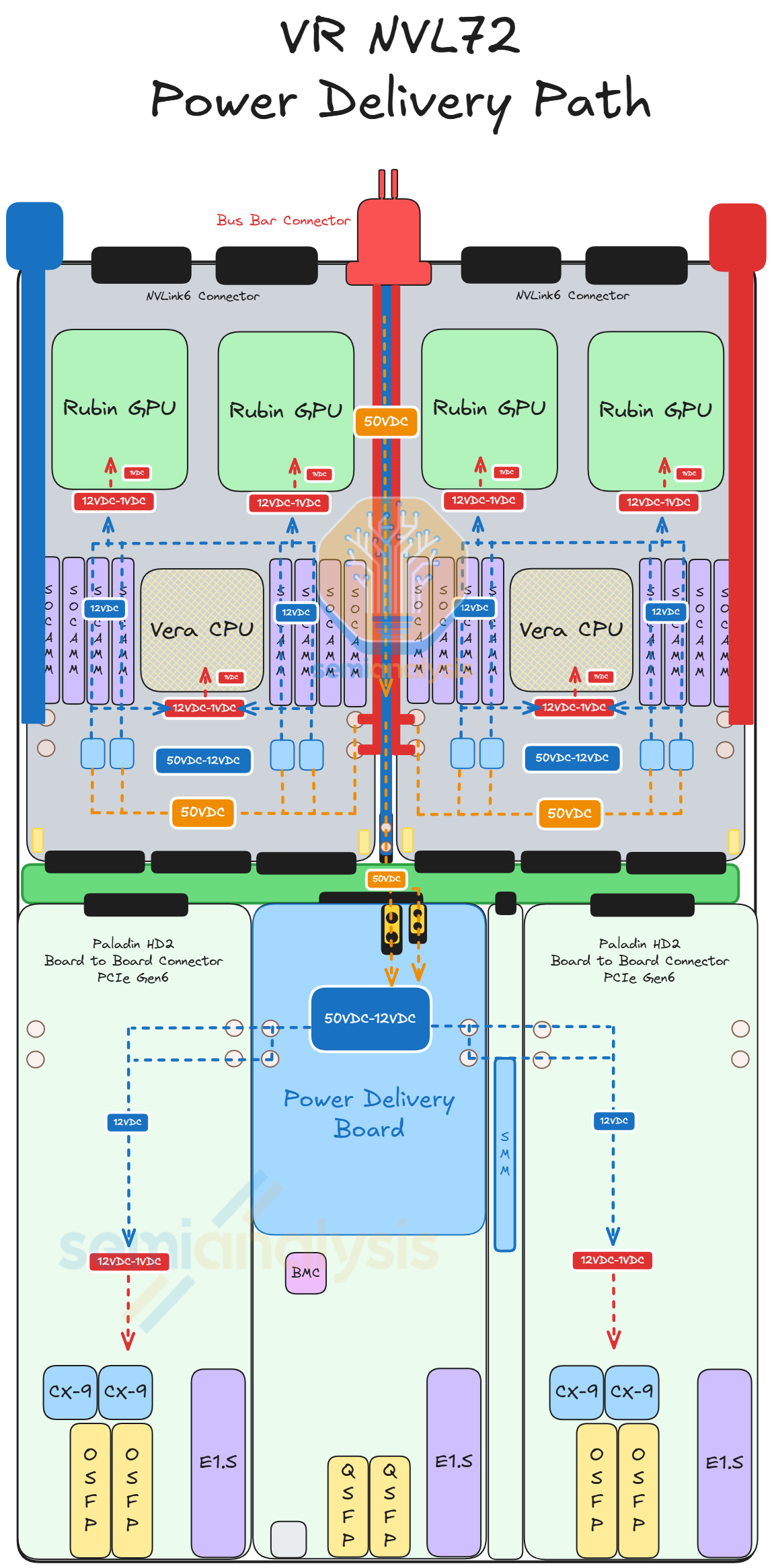
50VDC enters the Strata Board via one of the 50V power connectors on both sides of the Strata board. 50VDC is stepped down to 12VDC by the IBC module at the bottom of the Strata Board. Then the 12VDC will be stepped down to 1VDC by the VRM before feeding into the Rubin GPU and Vera CPU. Strata directly receives 50VDC whereas the Bianca board of Grace Blackwell receives 12VDC from the PDB. As the Strata board draws around 4800W of power (equivalent to the TDP of half a general server rack) versus Bianca at 3000W, it is necessary to deliver power to the board at a higher voltage. The benefit of moving 50VDC-12VDC conversion closer is to the reduce current and increase transmission efficiency. 96 Amps at 50V has 17x lower power loss than 400A at 12V due to the quadratic relationship between power loss and current.
We have the volume and ASP for all the power semis for the all the various VRMs contained in the VR NVL72 Component BoM and Power Budget Model.

Power sloshing between Vera and Rubin is still present, a feature carried over from GB300 that we covered in our article above. This enables more efficient power planning by sharing the 4800W provided amongst both GPU and CPU. In GPU demanding loads, 2300W goes to each GPU leaving 200W for the CPU. Vera can then dynamically boost to higher power when GPU demand drops to help minimize GPU idle time while not overprovisioning power.
For the modules at the front of chassis - CX-9,BlueField-4, and management - the PDB feeds 12VDC of power to each of the modules. 50VDC l down to 12VDC at the PDB then, via a coper busbar device, the PDB feeds 12VDC to its neighboring modules. The power connector of CX-9 is located near the Paladin HD2 at the top of the modules.
Compute Tray: Mechanical
The mechanical components of the VR NVL72 compute tray are slightly more sophisticated than that of the Grace Blackwell. At the front of the chassis, there is a mechanical structure that separates the front into three sections, with the left and right sections housing the Orchid modules and the middle sections housing the BlueField-4, the power delivery and the management modules. Each of the modules will also have a small metal chassis. The mechanical structure provides a simple guiding mechanism that guides the modules to a blind mate process with the midplane and the internal manifolds.
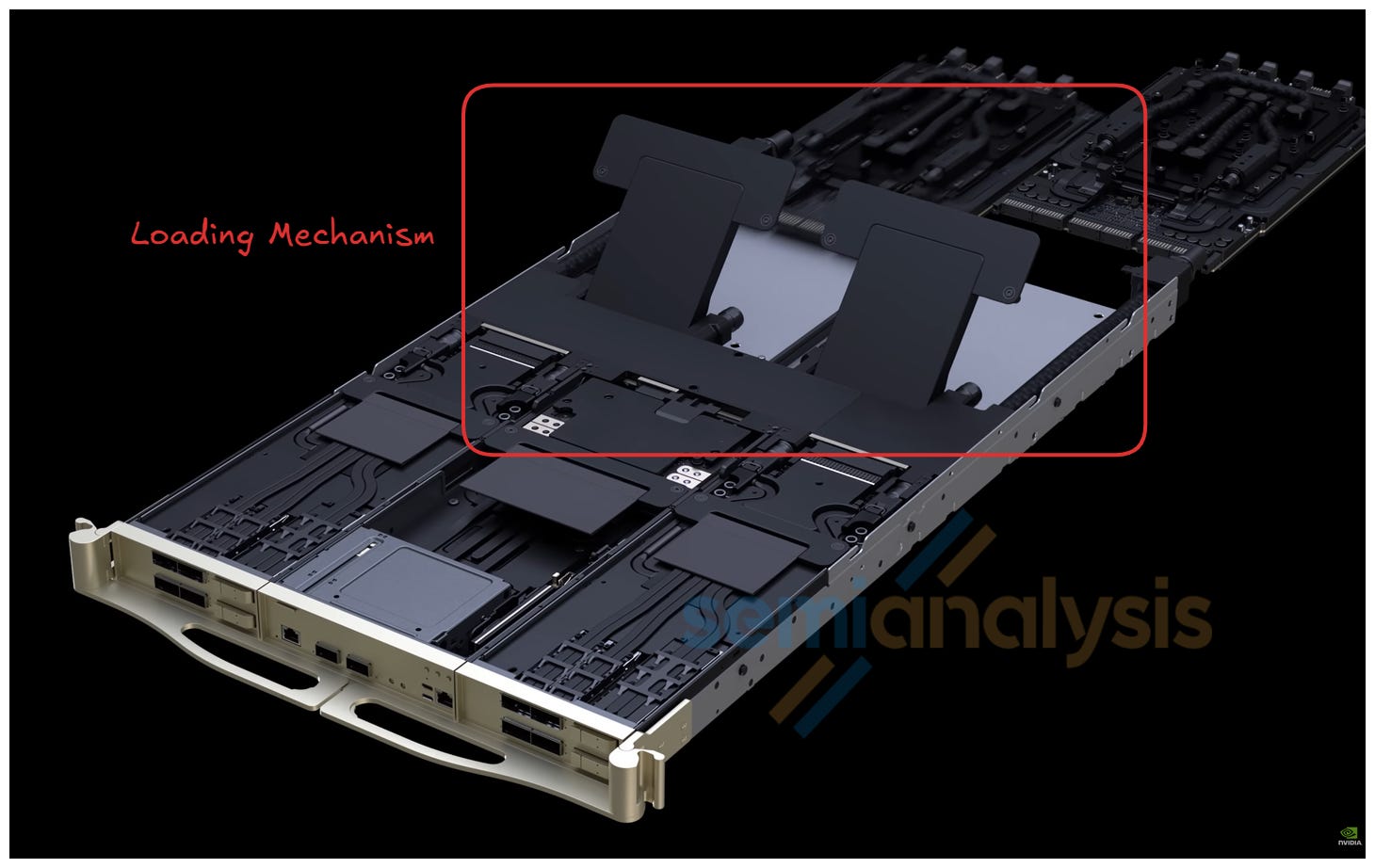
The midplane and the internal manifolds are shipped together as a module. The mechanical design of this module is shown in the picture above. These highlighted mechanical parts acts as a loading mechanism for the modules. These loading mechanisms ensure the modules are well connected to the Paladin connectors and the MQD by applying some force to the modules locking them in place.
Rack Level Infrastructure: Thermal
Beyond the redesigned fanless front chassis and the 100% liquid-cooled compute tray, the most notable point in the Vera Rubin cooling architecture discussion was Jensen’s comment on coolant/water warm temperatures and the use of chillers. For many (for Mr. Market more broadly!) the statement that Vera Rubin can operate with 45C inlet temperatures, potentially avoiding mechanical compressor-based chillers, was viewed as a major surprise for much of the cooling supplier ecosystem. We instead view this as a continuation of existing trends.
Vera Rubin will be able to operate at a 45C inlet temperature, but Blackwell is already capable of operating with inlet water temperatures above 40C (see for example Supermicro’s DLC-2 system). Major system vendors such as Lenovo and HPE have also been discussing 100% liquid-cooled architectures operating at 45C since early 2025. In 2024, HPE announced an industrial cooling system based on full liquid cooling, and similar approaches have long been used before in HPC. Lenovo discussed the next generation of its Neptune liquid solution at the 2025 OCP Summit, which is fully liquid-cooled and also uses 45C water.
Consider Schneider’s GB300 Reference Design 111, presented in September 2025, as another example. In this reference design, the datacenter uses a dual-loop architecture: a chilled-water loop dedicated to air cooling (feeding the fan walls) and a separate, higher-temperature loop dedicated to liquid cooling. On the liquid side, the TCS circulates coolant to the cold plates at roughly 40C and returns it at a higher temperature, while the CDU transfers that heat into the facility water loop, which can enter the CDU at approximately 37C.
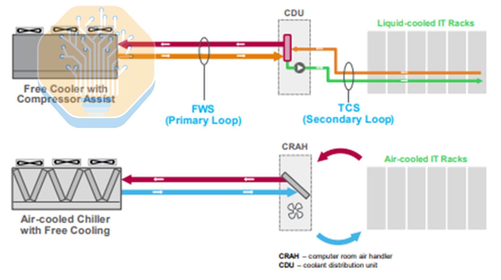
So 45C cooling is not entirely new. Even with this capability, most operators deploying Blackwell are still designing for 20-30C water temperatures. As a rough approximation, current Blackwell inlet temperatures are around room temperature, with outlet temperatures in the 40-50C range. Only a small number of operators, such as Firmus, have removed chillers from the loop (even with systems like GB200) in favor of highly optimized economizer designs where climate permits. Avoiding the compression step in mechanical cooling can deliver meaningful energy efficiency gains.
Now, how does Nvidia cool this heat monster, given that Vera Rubin’s power consumption and heat generation is roughly double that of Blackwell? Before answering, it is worth adding another consideration. Warmer inlet temperatures, while improving energy efficiency, can make cooling more challenging as inlet temperatures approach the maximum outlet temperature (the system’s ceiling temperature) and the delta-T tightens. With less temperature differential, you need higher water/coolant flow to remove the same amount of heat. In Blackwell reference architectures, the ceiling temperature is around 65C (e.g. see the Vertiv GB200 NVL72 reference design).
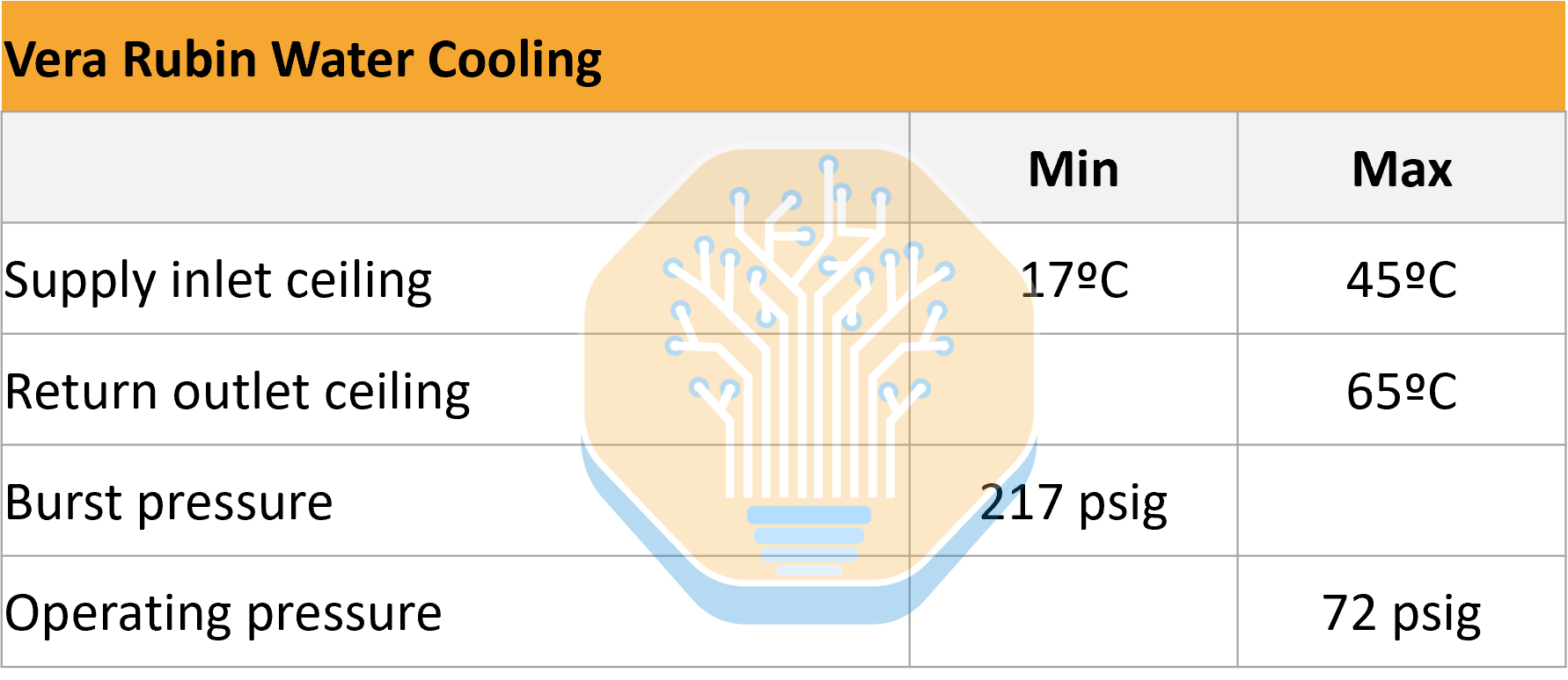
Although NVIDIA initially did not formally publish full specifications for Vera Rubin’s liquid cooling system, we believe the platform will support maximum coolant return temperatures up to 65C. This aligns with Nvidia’s warm-water operating envelope, and while the exact implication for delta-T depends on the chosen supply setpoint and flow control strategy, we can expect a slightly tighten delta-T. The pressure envelope is expected to be unchanged versus GB200, with maximum operating pressure of 72 psig (5 bar) and minimum burst pressure of 217 psig (15 bar), aligning with OCP’s MGX rack-level liquid-cooling specification.
In practice, cooling follows straightforward physics. To cool a system, you must deliver sufficient water/coolant at the appropriate temperature and pressure through the loop. If you want to increase the cooling capacity of a CDU, you increase flow rate while managing pressure, which in this case implies around a 2.0-2.5x flow increase, depending on how far outlet temperatures are actually pushed by operators.
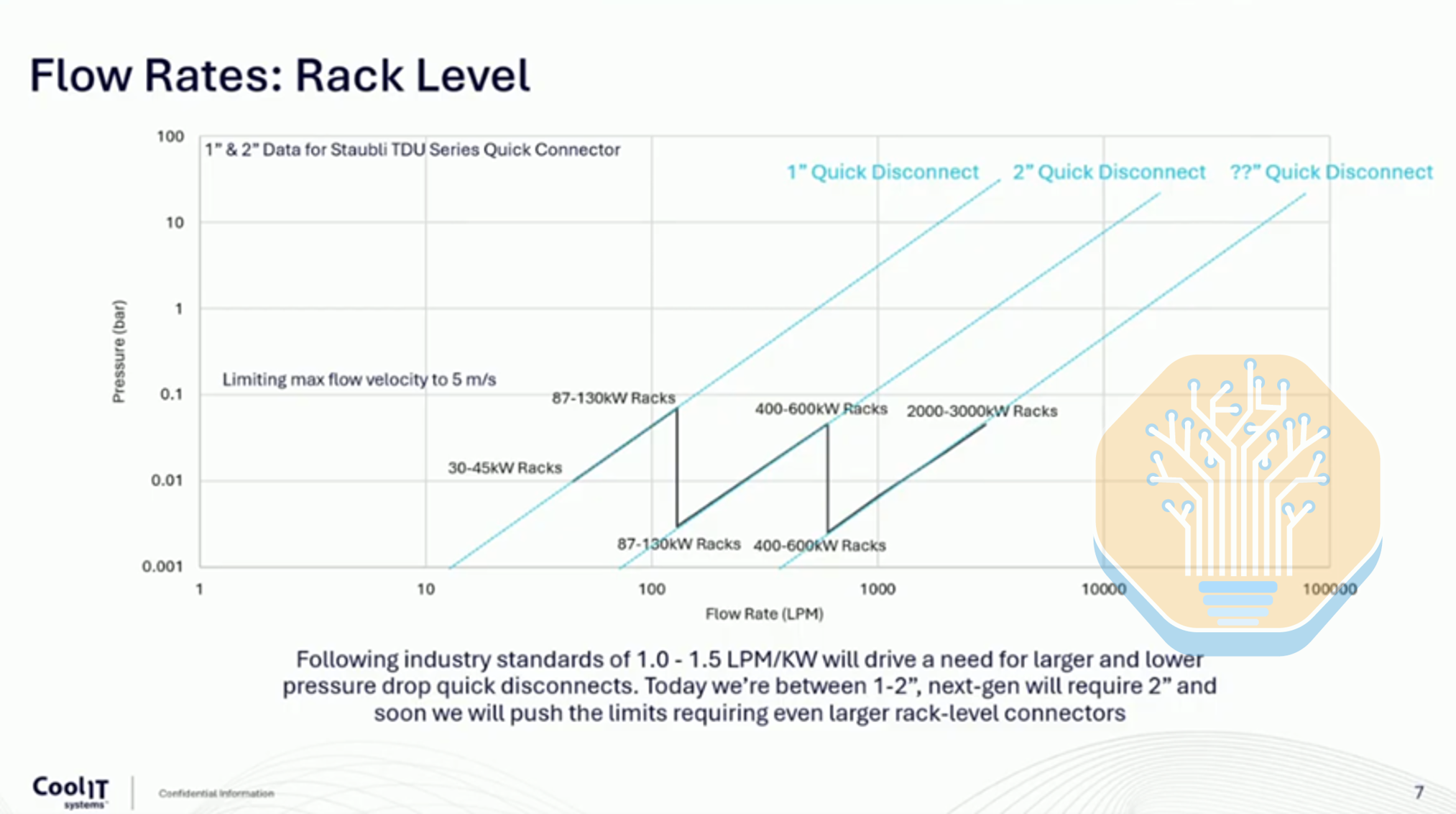
Nvidia has indicated that Vera Rubin increases liquid flow rate and achieves nearly double the thermal performance vs Blackwell, without increasing CDU pressure head or introducing additional cooling complexity or cost. Nvidia has achieved this by optimizing the entire hydraulic path. We expect larger quick disconnects to support higher flow, as well as updated manifolds and piping. As seen in the image below, vendor roadmaps suggest that, at least for the next generation of racks, 2 inch QDs should be sufficient to accommodate higher flow while staying within pressure and flow-velocity limits.
Procurement and Cooling Vendor Implications
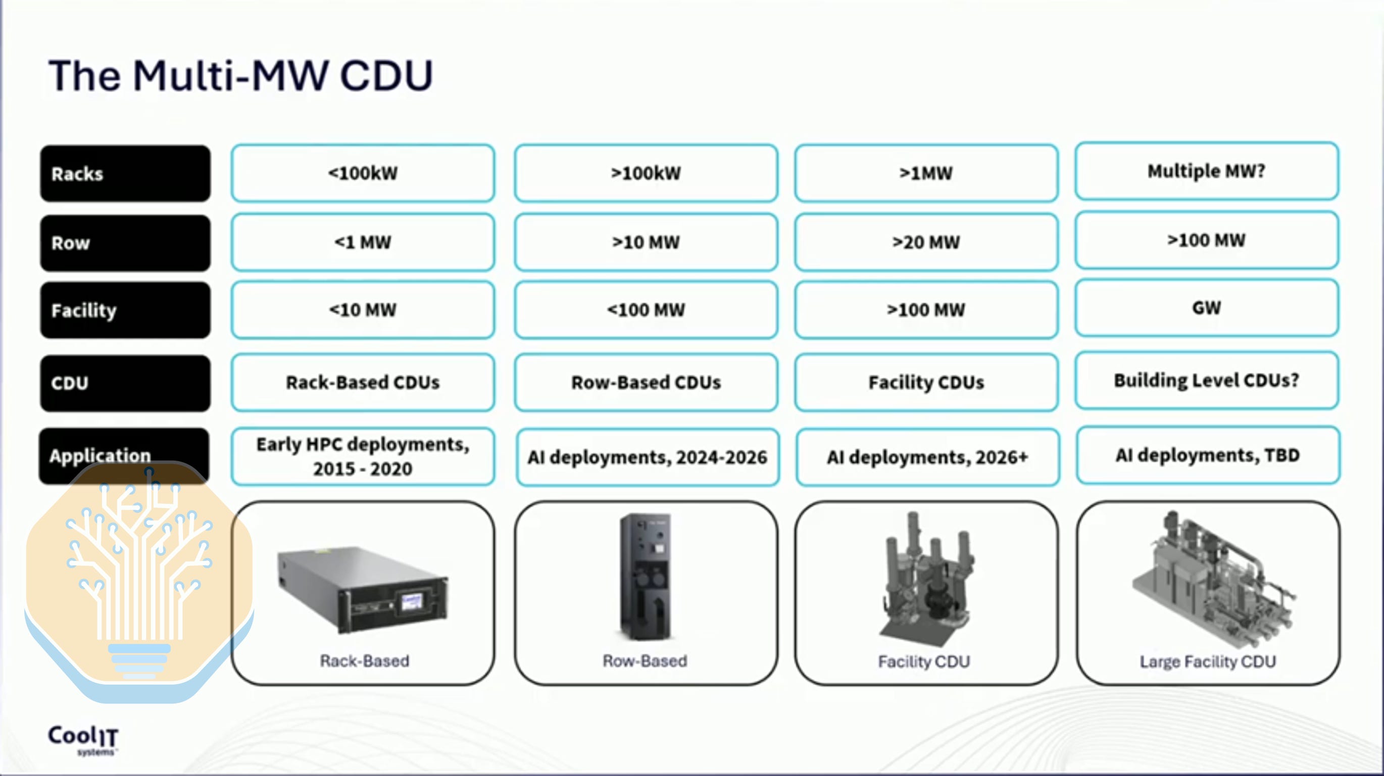
The primary vendor implication of the updated cooling architecture and doubled power density relates to CDUs and the rack-to-CDU ratio. Today, a CDU can support around 10 GB200 racks. With a rack generating about 2x the heat, that ratio would need to decline unless CDU capacity increases, implying either more CDUs or higher-capacity CDUs. We believe most major operators expect to maintain a ratio of around 10 racks per CDU. As rack power density rises, this points to larger CDUs. Today, in-row CDUs offer cooling capacities up to roughly 2 MW, but we expect future facility CDUs to reach 3-6 MW. Delta currently leads in the CDU specialist segment, alongside Schneider Electric, Vertiv, and nVent. Foxconn and Quanta dominate the system integrator category.
The shift from liquid + air to 100% liquid systems, combined with higher flow rates and greater cooling capacity, will require changes across the cooling stack. Fans and radiators used in L2A CDUs will become less critical over time. That said, L2A is likely to maintain meaningful share during the current upcycle, where deployment speed matters more than full optimization, though the long-term trajectory clearly favors L2L. High-density L2L systems will also require redesigns across much of the TCS. This includes updated manifolds, larger quick disconnects (Colder Products Company, Danfoss, Staubli, Parker Hannifin), gold-plated cold plates (AVC, Delta, Boyd, CoolIT, Auras) and, very critically, larger pumps capable of delivering the required water volume. Pump sizing is directly linked to power density and the heat that must be removed. Even manufacturers of motor and drive components used in these pumps, such as Allegro MicroSystems, could see their prospects change as either larger motors, more motors, or both are required. In summary, higher heat on the TCS loop likely increases content/MW for white-space cooling vendors. QDs should benefit most, alongside manifolds and cold plates, with CDUs also benefiting, though to a lesser extent.
For the FWS layout, the headline implication is the potential for chiller-less designs. While we addressed this debate in a separate explanatory note for our core research and datacenter model subscribers, we reiterate that this is not entirely disruptive. Some operators are already running Blackwell systems without chillers in more AI-optimized designs, while others choose to retain chillers for workload flexibility, mixed-hall compatibility, redundancy, and reliability. Over the long term, we expect AI-optimized systems to make chillers less necessary, with content shifting from air-cooled chillers toward dry coolers or adiabatic towers. We currently estimate roughly $0.5M/MW of air-cooled chiller content versus about $0.2M/MW for dry coolers or adiabatic towers. SPX Technologies, alongside BAC and Evapco, could benefit, while Johnson Controls, Carrier, and Trane may be challenged. Nonetheless, we expect this efficiency/flexibility trade-off to persist in the medium term and do not foresee a chiller downturn occurring overnight. See our Industrials Model for more details.
Rack Level Infrastructure: Power Delivery
In the GB200 article from 2024, we discussed the previous evolution on power delivery from node level PSU (power supply unit) to centralized rack level power shelf. As VR NVL72 rack TDP reaches 180kW-220kW per rack from 120kW-140kW for GB200 and GB300, the power delivery infrastructure has evolved yet again. In the section below we will discuss the power delivery infrastructure at the rack level of the reference design and the power delivery at the compute tray level for VR NVL72.
Since the deployment of GB200, the main theme of the power delivery infrastructure evolution has been about transmission efficiency and power stability. Hyperscalers are developing power delivery infrastructure to address the challenges that comes with high density AI server racks with the roadmap set to 1MW per rack in the next couple of years. Hence, HVDC (high voltage direct current) power rack, BBU (battery back up units), CBU (capacitor backup units), liquid cooled busbar, and SST (solid state transformers) are being developed to increase transmission efficiency and power stability. These will be deployed by customers depending on their proprietary infrastructure designs. For more detail on this, we wrote about the challenge on the grid with AI training in this report.

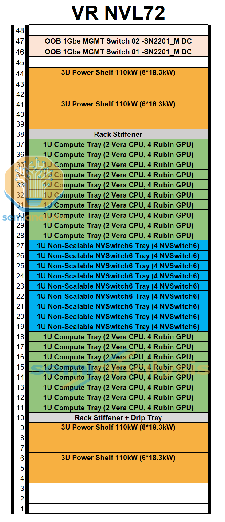
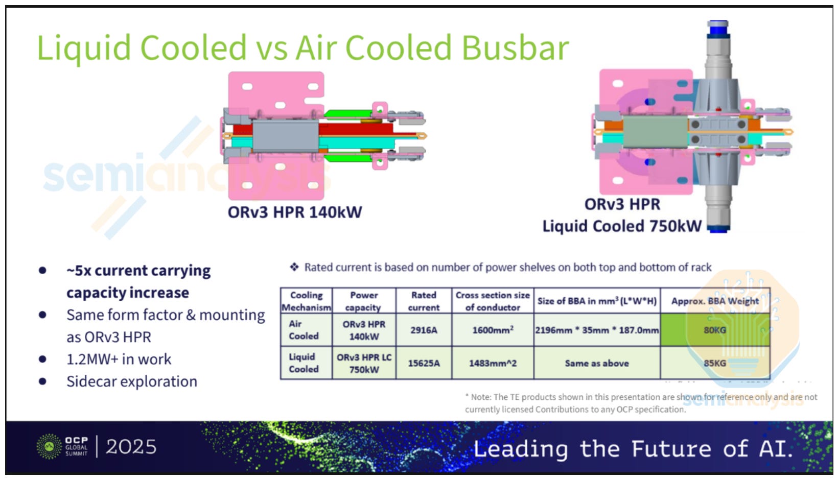
For the VR NVL72 reference design, the power delivery infrastructure at the rack level includes four 110kW power shelves. The VR NVL72 system has a TDP up to 220kW for the 2300W Rubin TDP SKU. The design with four 110kW power shelves is an N+1 redundancy approach. Each 110kW power shelf is 3U tall and includes six 18.3kW PSU with built in capacitors in the PSU. Each power shelf receives three phase 415VAC-480VAC of power from two 100A whips. The power shelves step down the power from 415VAC-480VAC to 50VDC and sends it to the busbar. Interestingly, the busbar of VR NVL72 is rated for 5000A+, which is much higher than that of Grace Blackwell at 2900A. Given the extremely high current and the lack of fans in the rack, the busbar has to be liquid cooled.
For the hyperscale customers, they might choose to deploy a standalone power rack either in LVDC (low voltage direct current) or HVDC (high voltage direct current). Below we provide two possible scenarios of the power rack deployment for VR NVL72.
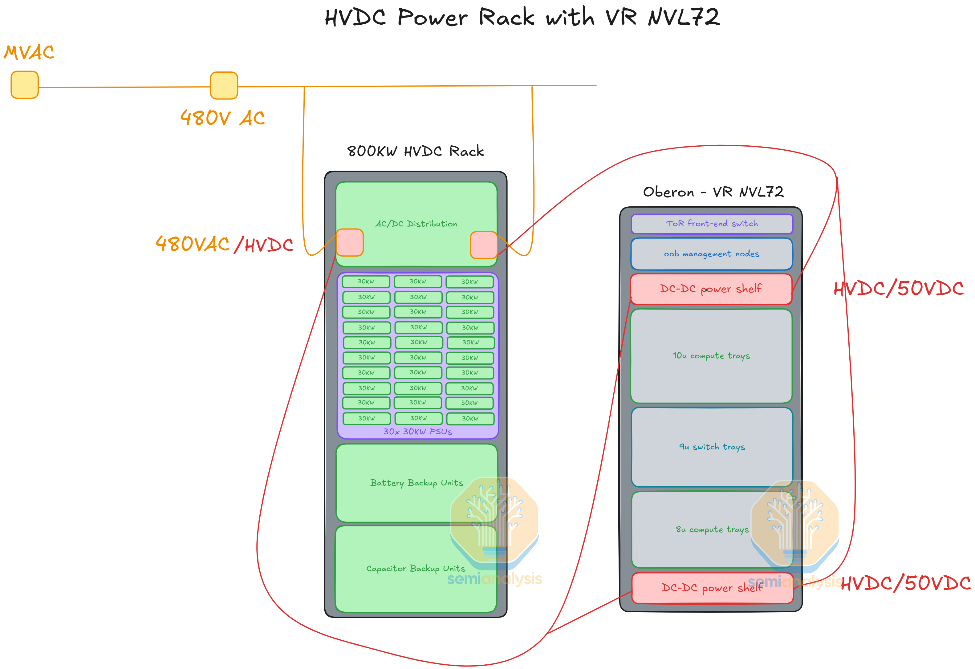
First, VR NVL72 rack with an HVDC power rack running at 800VDC (Nvidia Spec) or +/-400VDC (OCP Spec). Since the VR NVL72 rack busbar is still running at 50V and the compute tray can only take in 50V, the 800VDC from the power rack cannot be directly delivered to the busbar. There would still be DC-DC power shelves in the VR NVL72 rack. The DC-DC power shelves will step down the voltage of the current from 800VDC to 50VDC as demonstrated below.

Second, some customers, namely Meta, may look to integrate their network switch rack with BBU and CBU shelves for efficiency and peak shaving. This allows more CBU and BBU capacity that wouldn’t have been able to fit in the GPU rack. The BBU/CBU and switch rack will be connected to the GPU rack with 50V horizontal busbars. Meta calls this the high power rack, discussed at OCP.
We have more detailed power and architecture details in our VR NVL72 Component BoM and Power Budget Model.
Networking: NVLink 6, Rubin Scale Out
NVIDIA’s gen-on-gen innovations are evolutionary and not revolutionary. With GPU scale-up and scale-out bandwidth doubling approximately every 18 months, the copper infrastructure in NVIDIA racks are being innovated to accommodate higher bandwidth workloads. Scale-up network infrastructure will eventually involve optics to build larger world sizes, but that is the topic of a separate article.
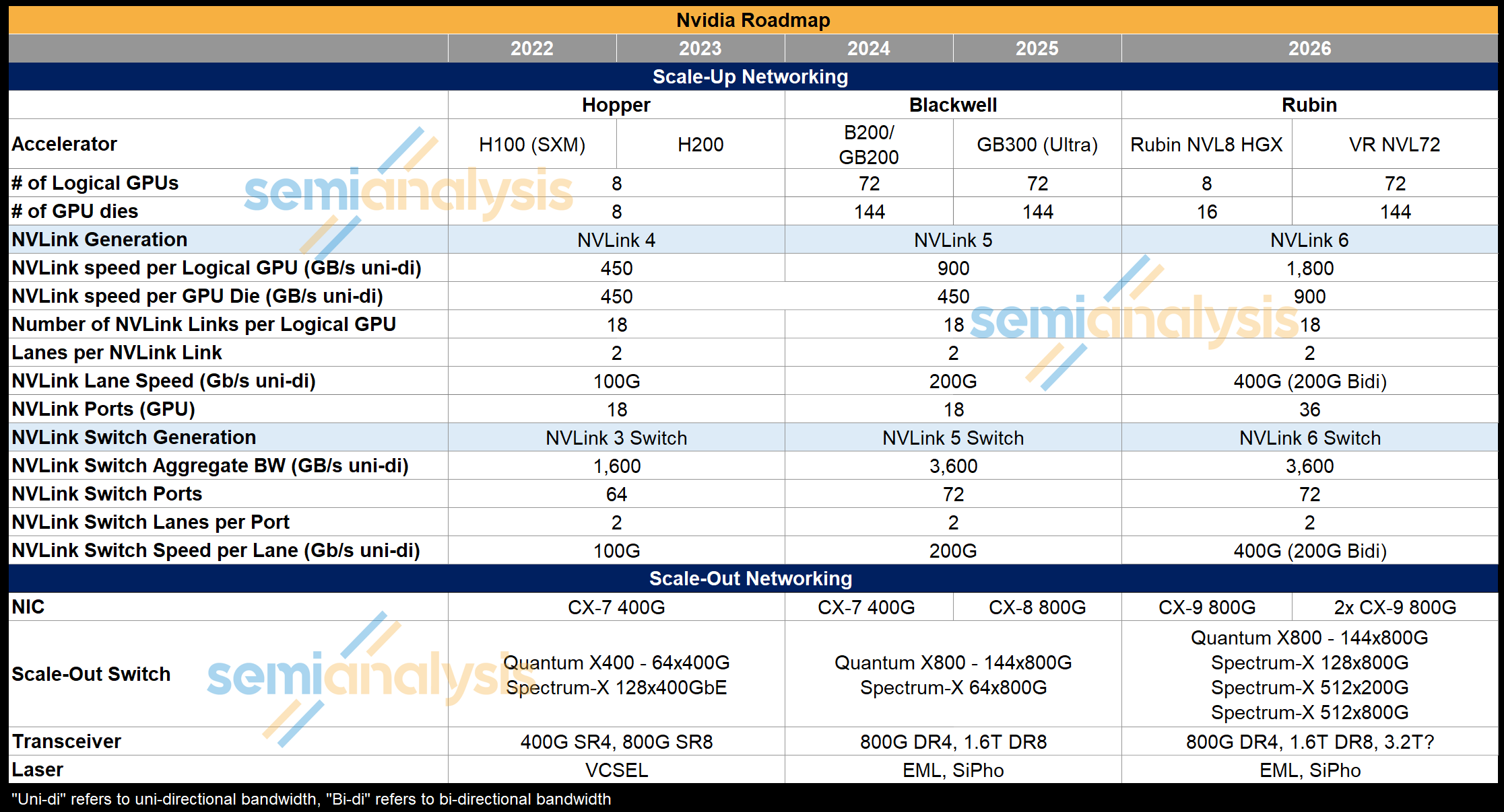
The below table shows the evolution of scale-up and scale-out networking speeds. NVLink 6 used in Vera Rubin doubles NVLink bandwidth by implementing bi-directional signaling over the same number of copper cables - effectively delivering 4 Lanes of 200G per NVLink. Much more on this in the following sections.
Let’s step through key features of Rubin’s networking and the architectures that are likely to be built around Rubin scale-up and scale-out networks.
Bi-directional SerDes for Scale-Up
The doubling of bandwidth per logical GPU from NVLink 5 in GB300 NVL72 to NVLink 6 in Vera Rubin NVL72 are made possible by using a simultaneous bi-directional SerDes for the copper backplane instead of increasing the modulation or baud rate. Whereas NVLink 5 delivers 224G per electrical lane, NVLink 6.0 delivers 448G per electrical lane. Each electrical lane is one differential pair (DP) consisting of two conductors that carry equal magnitude, and opposite polarity signals.
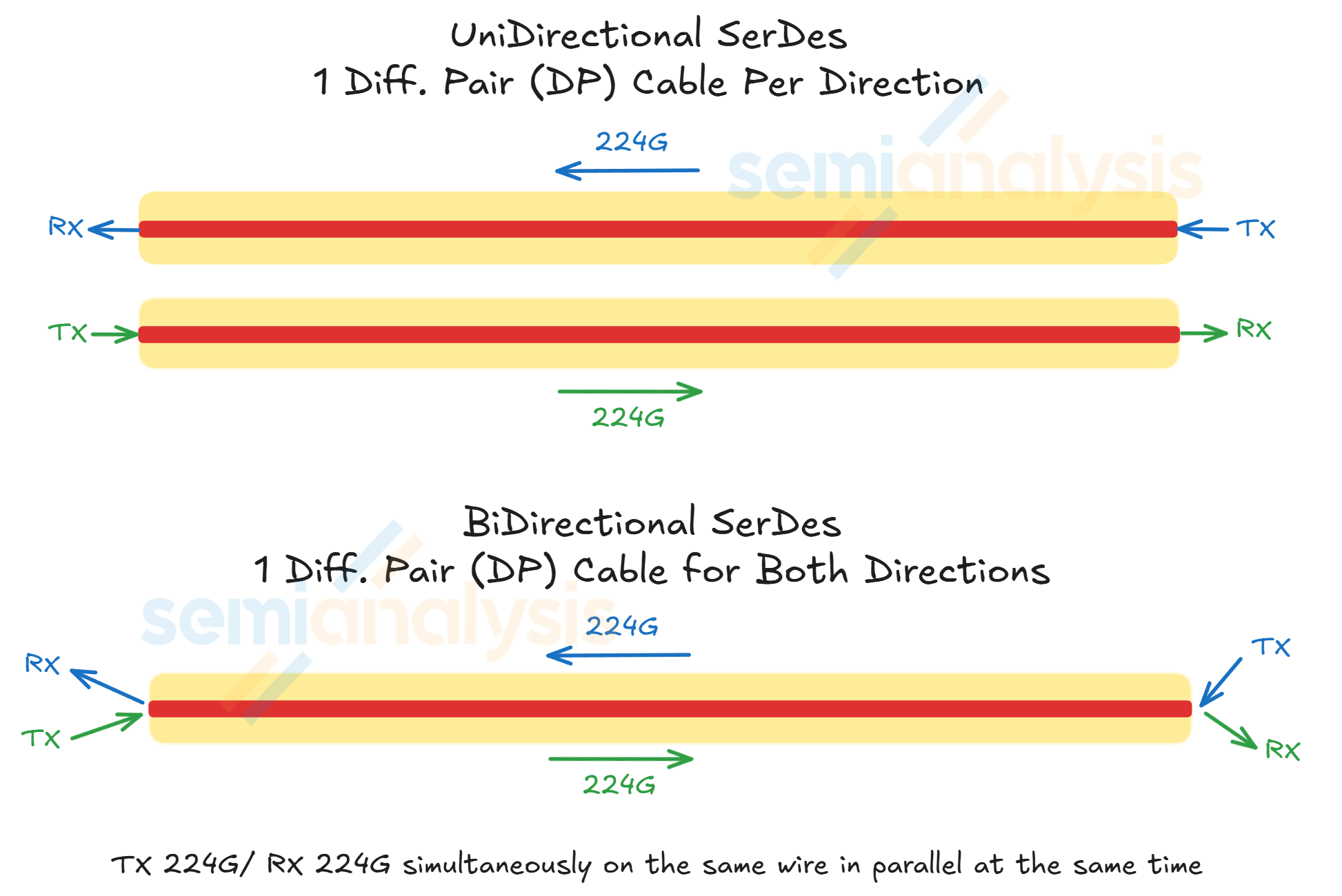
This gives rise to the engineering problem of ensuring that a clean signal can be received at either end of the wire because two signals sent in opposite directions over the same copper wire will superpose to form a composite signal that is different from the intended transmitting signal.
In optics, bidirectional interconnect can be achieved by integrating an optical circulator to a transceiver as discussed in our TPUv7 article published late last year. The circulator works by routing the inbound and outbound signal onto separate paths, ensuring no overlaps between both at the photodiode receiver. Bidirectional interconnect is, however, much trickier in the copper domain. A circulator cannot be used as copper cables are linear transmission lines, which means that the inbound and outbound signals will be summed at the receiver through superposition. The receiver at each end of the copper wire therefore needs a mechanism to separate the local TX from the local RX.
The solution to this problem is the use of a hybrid at each end of the wire. Without a hybrid, there will be self-interference at the local RX because both the local TX and local RX are being transmitted along the same wire:
An inverted copy of the local TX must therefore be generated at the local RX for proper echo cancellation:
The diagram below illustrates this dynamic:
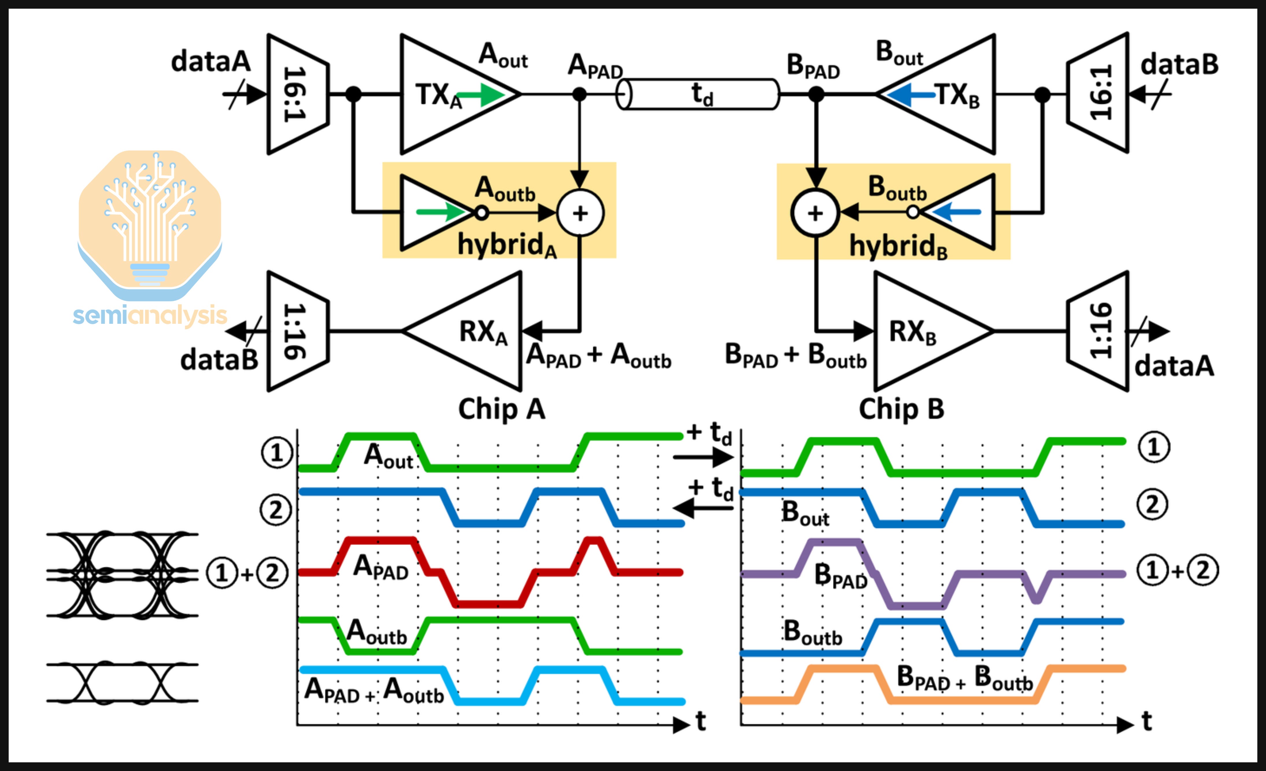
While bidirectional signaling is being used for short-reach (less than 5mm) die-to-die interconnect, what stands out is that NVIDIA has extended this technology to longer reach transmission over copper backplane with a reach of at least 1m.
The challenge with bidirectional signaling is that echo cancellation must be precisely calibrated or slight delays in the generation of the local TX copy can cause link failure. However, if NVIDIA were to continue using the 200G SerDes, doubling the bandwidth would mean doubling the number of copper cables at the backplane, which is a tall order for several reasons.
Cramming in approximately five thousand copper cables on the backplane at the Blackwell generation has introduced non-trivial reliability failure modes at scale. To double scale-up bandwidth while staying on regular 200G SerDes would require the backplane to double to ten thousand copper cables: only further increasing the manufacturing complexity and likelihood of failure of the system.
NVIDIA could also opt to deploy wider racks instead as is the case of AMD’s Helios rack, but this could affect the signal integrity on the PCB as electrical signals will have to traverse a longer path.
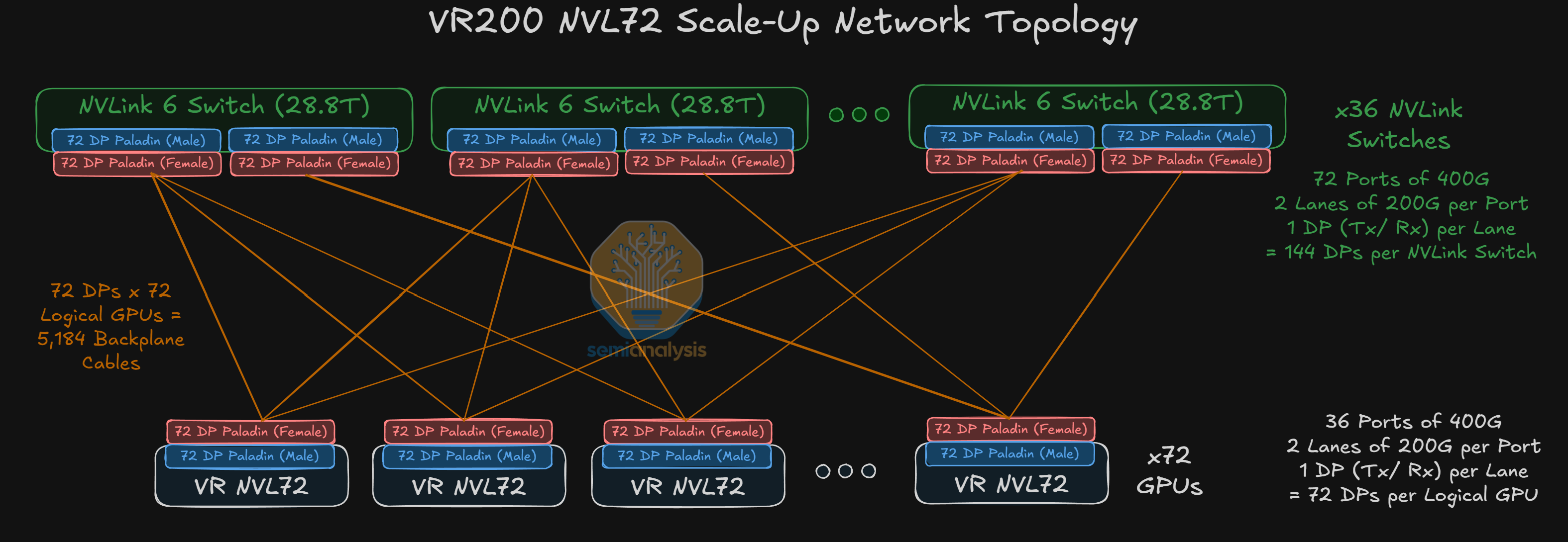
Scale-Up Network – NVLink 6
The bidirectional SerDes technology employed on the copper backplane is used for NVIDIA’s scale-up network. For Vera Rubin NVL72, the scale-up network continues to be rail-optimized with all-to-all connectivity between each GPU and switch ASIC in the scale-up domain.
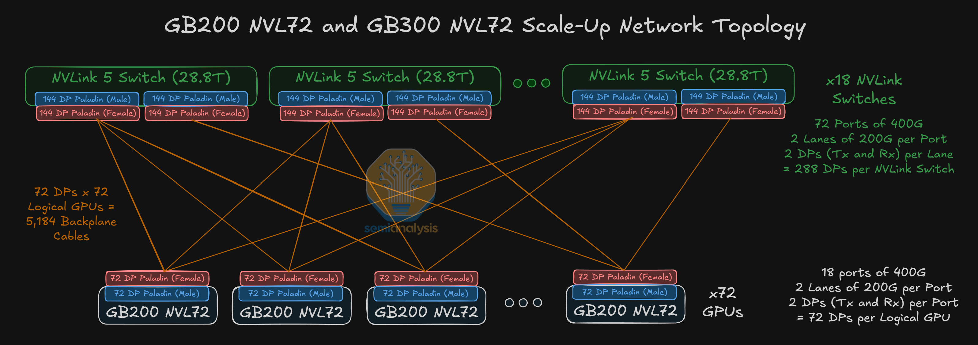
Last year, we discussed NVIDIA’s GB200 scale-up architecture, which consists of 18 NVLink 5 Switch chips in a single rack for the NVL72 system.

Although the NVLink 6 Switch used in the VR NVL72 system delivers the same per switch 28.8T aggregate bandwidth as NVLink 5 Switch, the SerDes speed on the NVLink 6 Switch is double the SerDes speed of NVLink 5 Switch but with the same number of DPs. As such, in order to deliver double the aggregate scale-up bandwidth required for NVLink 6, Vera Rubin NVL72 racks will contain double the number of NVLink Switches as compared to GB200 racks. This translates to four NVLink Switch chips per tray on 9 switch trays, or 36 NVLink Switch chips in each rack.
Each VR NVL72 Switch tray contains four NVLink 6 Switch ASICs and one system management module. The design of the Rubin NVLink 6 Switch tray is also simpler and relatively seamless compared to the first Oberon NVLink 5 Switch released for GB200 because Rubin NVLink 6 Switch trays will not use flyover cables. As such, all NVLink signals will run over the PCB.
The NVLink 6 Switch board is liquid cooled and will be covered with a cold plate, which is a single module. Connected to the NVSwitch tray is the system management module (SMM) that comes with a CPU and acts as a host to the switch tray. The switch tray to SMM connection uses flyover cables, but this is the only flyover cable connection required in the entire Vera Rubin NVL72 system. Given that the PCIe connection is lower speed and the NVLink Switch tray contains relatively few modules, assembly of the switch tray is unlikely to be challenging.
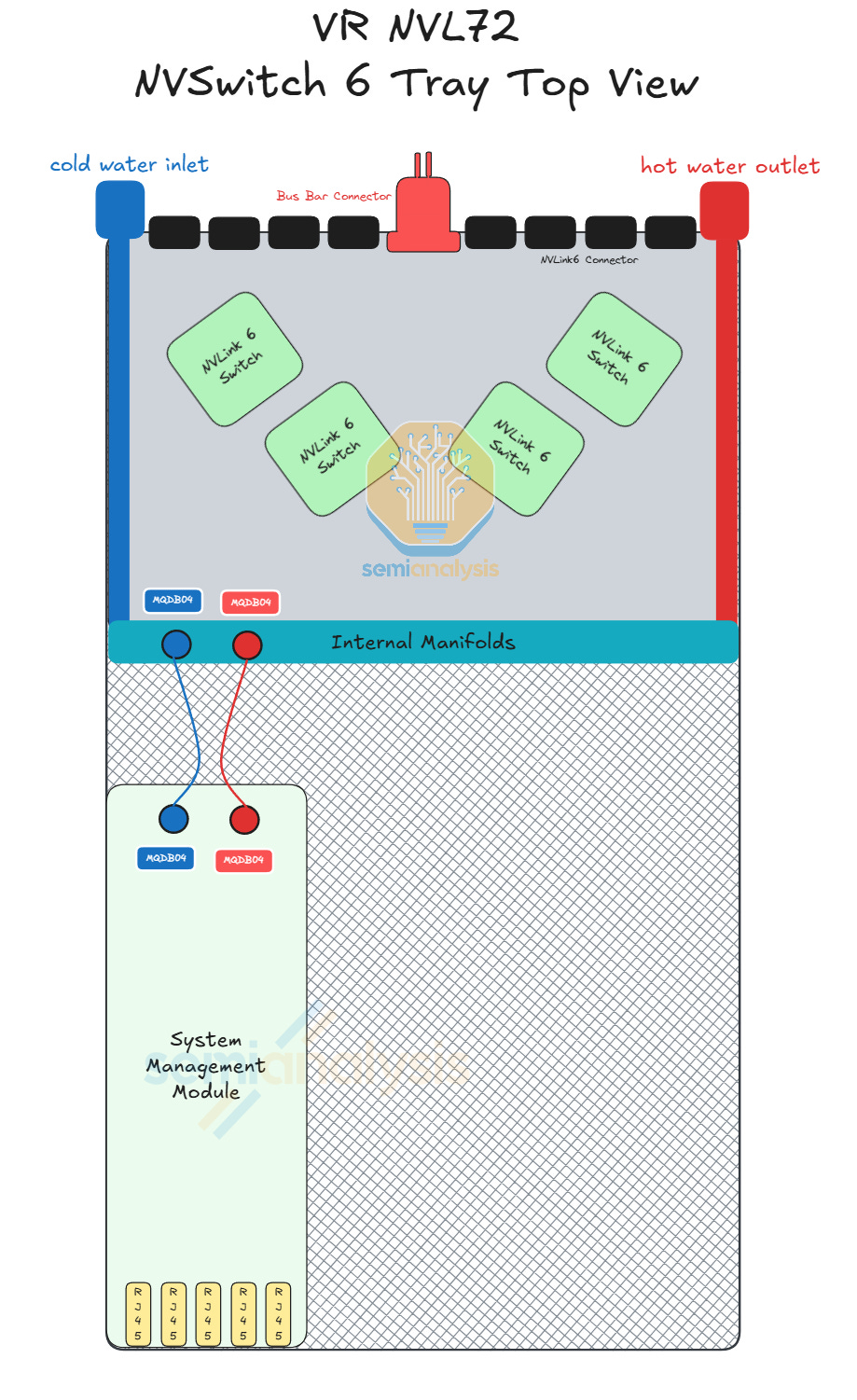
The diagram below shows how the NVLink 6 signal traverses through the tray. Each of the green lines represents nine 400G logical ports of NVLink 6, or 18 TX/RX lanes of 200G. Because there is only 1 DP per lane using bidirectional SerDes, there are a total of 18 DPs between any connector and any switch for a total of 72 DPs per connector, which is the same as prior generation of NVLink 5 Switch Tray.
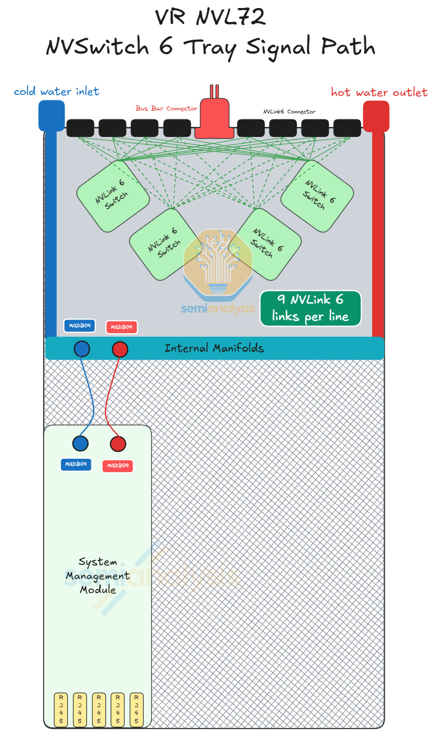
As previously explained, high speed signals require better PCB materials, especially for NVLink 6 which has much lower tolerance for insertion loss given the use of bidirectional signaling. The number of lanes between the PaladinHD2 connectors and the NVLink Switch also creates complexity for PCB design. Hence, the NVLink 6 Switch board PCB is upgraded to 32 layers with M8+ graded CCL - minimally LDK2 glass fiber cloth or potentially Quartz fiber cloth.
We have more details on the switch tray and various components in the VR NVL72 Component BoM and Power Budget Model.
Zooming out, backplane copper cables are used to connect NVLink Switch trays to the GPU trays for the VR NVL72 system. Although the bandwidth doubles, with bi-directional SerDes, the number of cables required does not change from the GB300 backplane generation to the Vera Rubin NVL72 backplane generation. The number of connectors and the number of DPs per connector also does not change from Grace Blackwell NVL72 to VR NVL72.
While the VR NVL72 system features GPUs and scale-up switches that are connected by copper cables, the VR HGX system features servers consisting of eight Rubin GPUs and four NVLink Switch chips. The second meaningful difference between the NVL72 and HGX deployments is that the former has a scale-out bandwidth of 1.6T per GPU while the latter only has a scale-out bandwidth of 800G per GPU. How is it that all Rubin 200 deployments use CX-9 NICs even though some deployments have half the per GPU scale-out bandwidth?
The HGX Rubin NVL8 server consists of eight 800G CX-9 NIC packages – one NIC per GPU – which means that the scale-out bandwidth does not increase from its predecessor, the HGX B300 server. The Vera Rubin NVL72 deployment on the other hand doubles the per GPU scale-out bandwidth to 1.6T, but not by doubling the bandwidth per NIC. Rather, the “1.6T NIC” attached to each Rubin chip is comprised of two 800G CX-9 packages that is connected to the Vera CPU by PCIe Gen 6.0 lanes.
Each compute tray on the VR NVL72 has eight 800G CX-9 NICs, but there are two possibilities for the number of OSFP cages - either one 1.6T OSFP cage per GPU for a total of 4 per compute tray, or two 800G OSFP cages per GPU for a total of 8 cages per compute tray. We think that the latter would be the more popular deployment assumption, and will be the base case for our discussion of scale-out networking architectures in later sections of the article.
Connecting GPUs in the Scale-Out InfiniBand Network
Broadly, there are three flavors of scale-out deployments for Vera Rubin NVL72. We have InfiniBand-based clusters which employ the NVIDIA Quantum series of switches, NVIDIA Ethernet-based clusters employing Spectrum series switches and lastly, non-Nvidia Ethernet such as Tomahawk-based, Cisco Silicon One or Teralynx-based Ethernet switches. Some Ethernet-based clusters deployed by hyperscalers will use AECs for NIC-to-TOR and switch-to-switch connections, while other Ethernet-based clusters using only optical interconnects will usually adopt a multi-plane and multi-rail networking architecture. What is particularly noteworthy about Vera Rubin NVL72 deployments, however, is that it is the first Nvidia GPU generation where we will be seeing some Co-Packaged-Optics (CPO) deployments in the scale-out backend network.
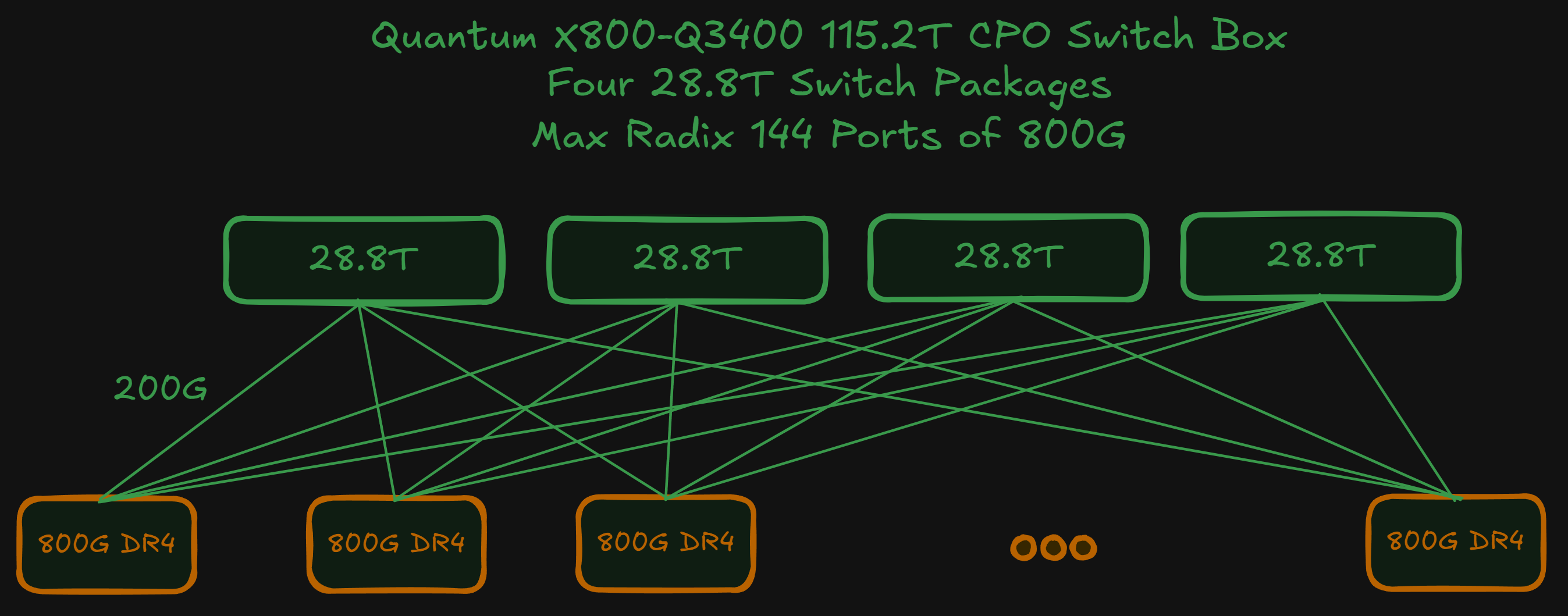
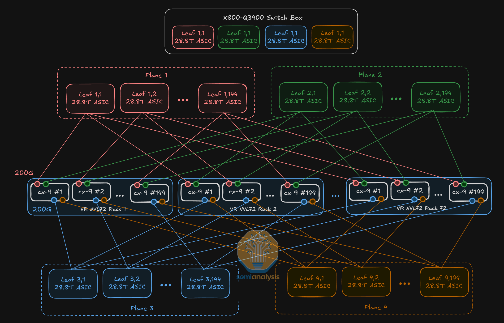
While there are both InfiniBand and Spectrum-X based clusters, the InfiniBand-based Quantum X800-34XX series of switches is more popular with Neoclouds than with hyperscalers. For InfiniBand, there are two deployment types – the first is the Quantum X800-Q3400 with pluggable optics and the second is the Quantum X800-Q3450 CPO-based switch that use co-packaged Optical Engines (OE) instead of pluggable transceivers.
The Quantum X800-Q3400 is logically a multi-plane switch combining 4 Quantum-3 ASICs into a single switch box, though we will dive into this equivalence later in the article. This multi-plane “topology” is abstracted away and as far as network engineers are concerned, the Q3400 is a single switch with 144 ports – or a “little boy” switch.
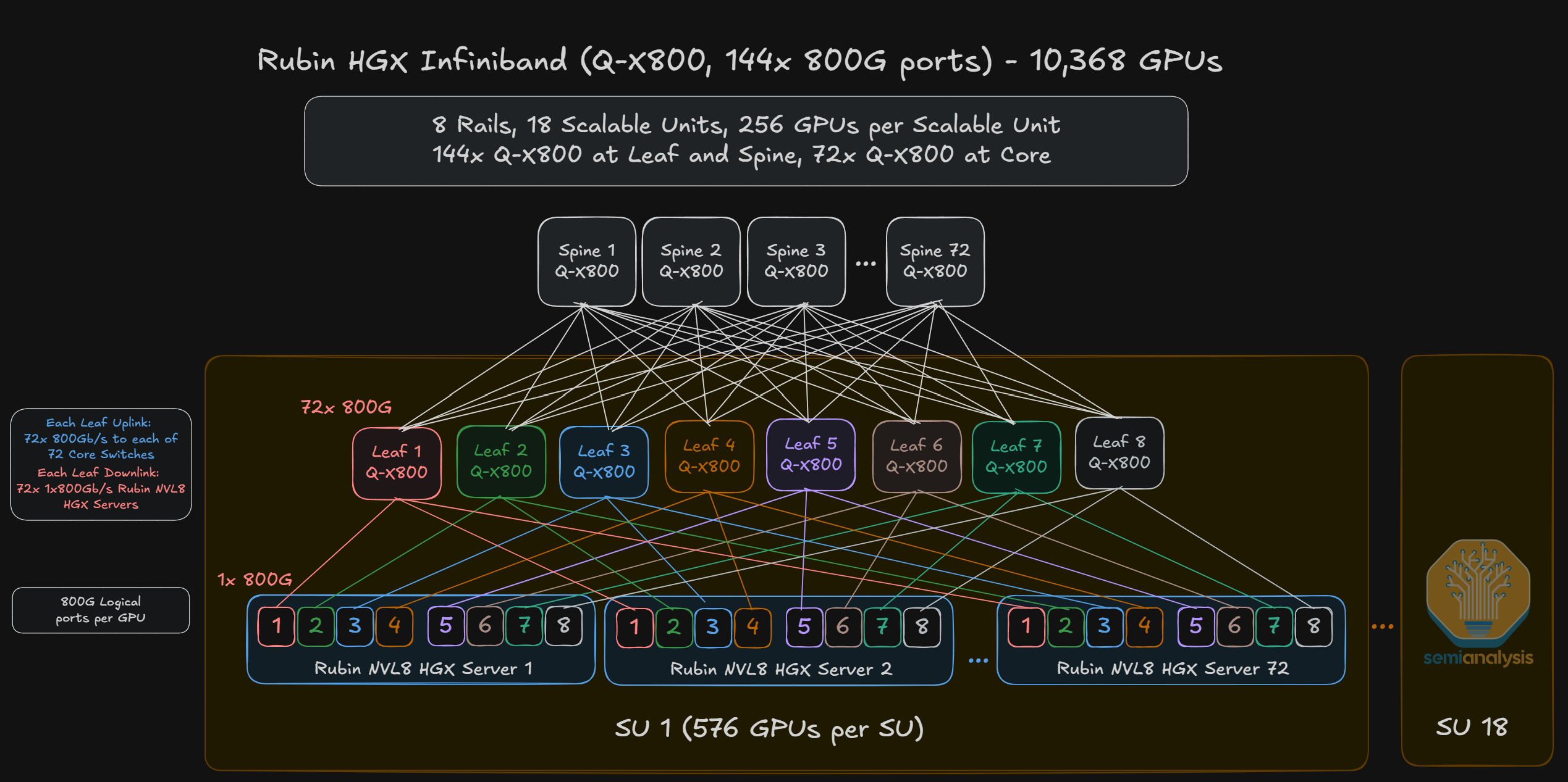
The InfiniBand architecture for the HGX Rubin NVL8 server is therefore effectively a single-plane, 8-rail network consisting of one 800G uplink from each HGX Rubin NVL8 GPU to a leaf switch.
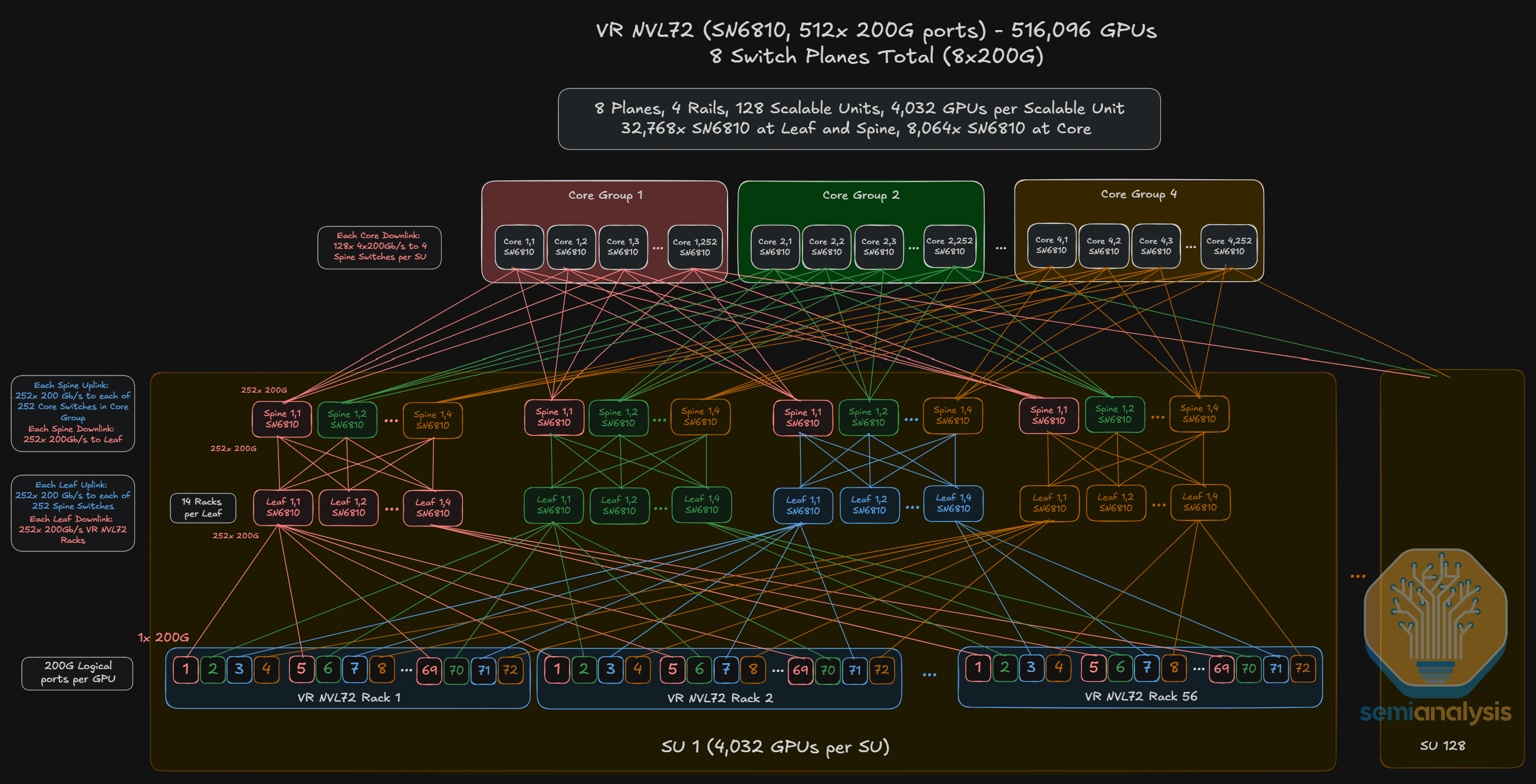
For the Vera Rubin NVL72 deployment however, there are two 800G OSFP cages per GPU for a total of 1.6T per GPU bandwidth. Having two 800G logical ports per GPU is advantageous because it allows multi-plane network deployments without complex fiber management – by splitting one logical GPU two ways to two different leaf switches. As such, larger network clusters can be built with two 800G logical ports than if only one 1.6T logical port were used. In fact, as we have explained in multiple prior articles such as the networking sections of NVIDIA’s Optical Boogeyman and Microsoft’s AI Strategy Deconstructed, this relationship is dictated by a simple formula for the maximum number of hosts that can be supported using a switch of k ports on an L-layer:
Illustratively, consider two hypothetical VR NVL deployments with 1.6T and 800G logical ports respectively. A 1-plane, 3-layer network with one 1.6T logical ports achieves only a maximum cluster size of 93,312 GPUs, or:
By one 1.6T logical port, we mean that the two 800G OSFP cages connected to each GPU are connected to a single, dual-port 1.6T transceiver at the leaf layer because the two 800G ports are effectively performing the function of one 1.6T port – and hence the term “logical”.
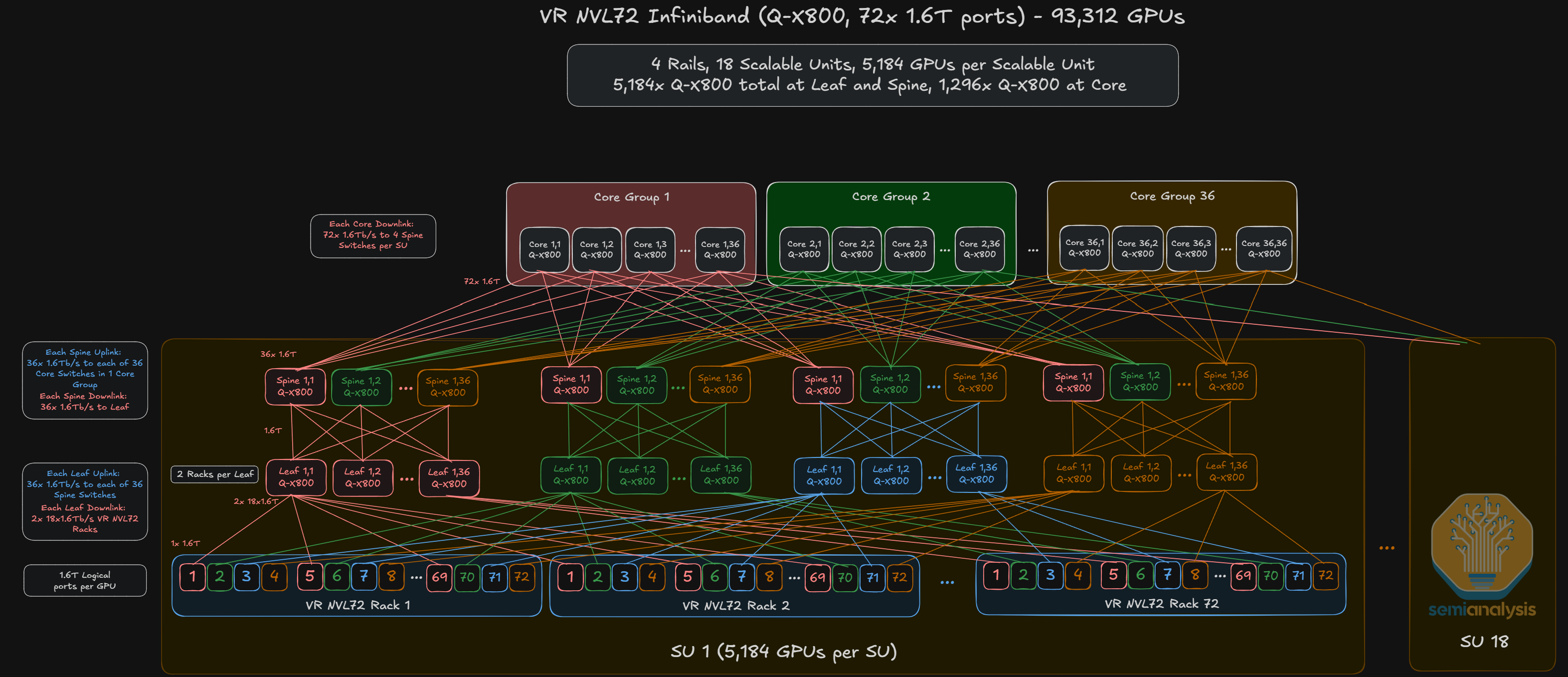
To scale beyond the maximum cluster size of 93,312 GPUs, a 2-plane network can be deployed in which each of the two 800G OSFP cages supporting a GPU are linked to separate leaf switches on different network plans. This allows you to build a 186,624-GPU cluster size as diagrammed below and even scale up to 746,496-GPU cluster sizes.
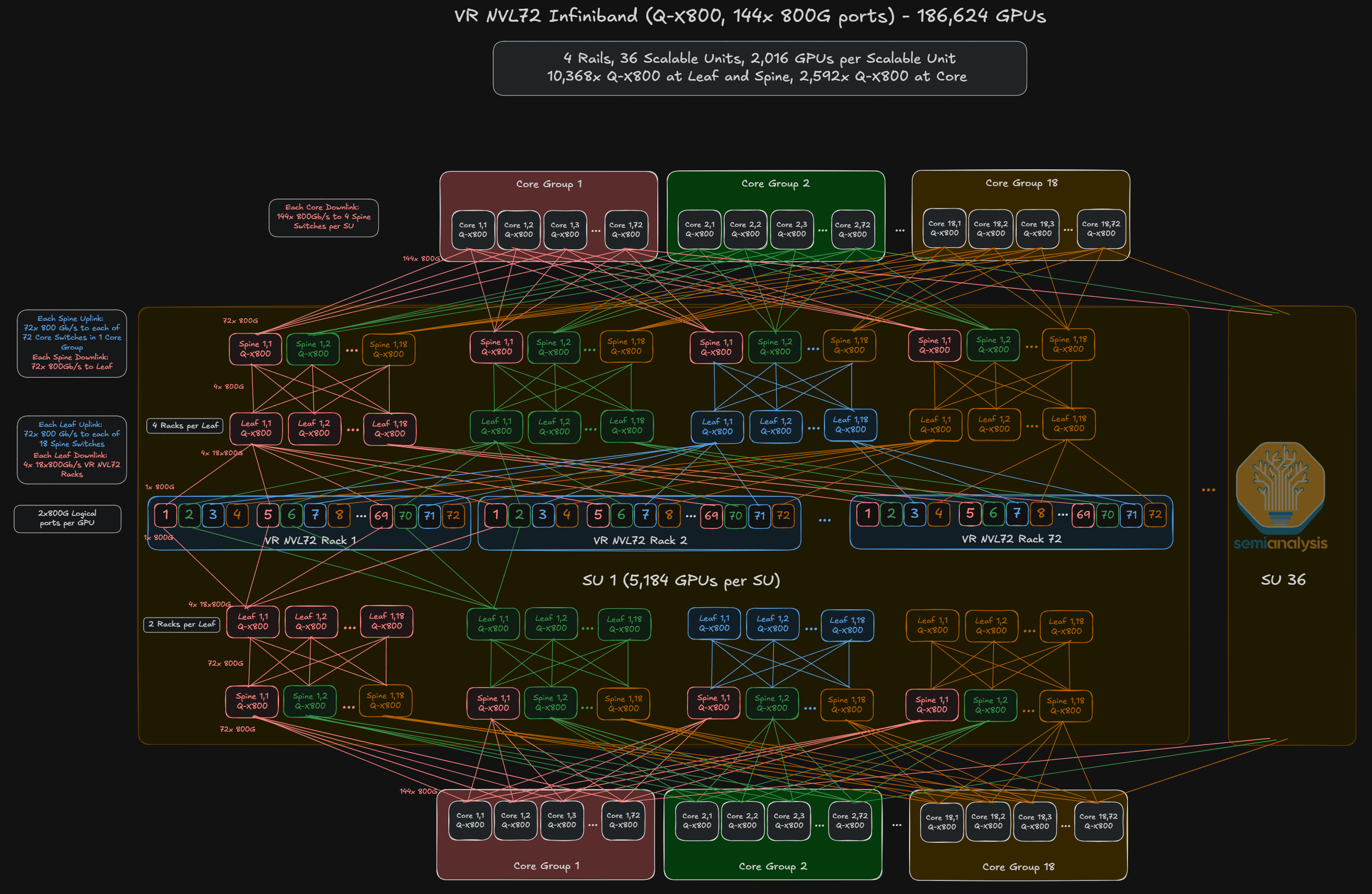
We think the second cluster with two switch planes will likely be the more prevalent reference architecture for Vera Rubin NVL72 InfiniBand deployments.
Aside from the X800-Q3400 air-cooled switch, NVIDIA will also offer a CPO version, which is the X800-Q3450 containing the same 144 ports of 800G. As pointed out earlier, what is unique about both switches is that each switch box consists of four 28.8T Quantum-3 Switch ASICs for a total of 115.2T per box switching capacity. When used in conjunction with the VR NVL72 servers, the signal from the NIC at the leaf layer is split four ways – 200G each way – to each switch ASIC within the box. Such a configuration bears logical equivalence to a 4-plane network architecture.
Ethernet-Based Cluster Deployments
Although InfiniBand has been the more popular network architecture for previous NVIDIA chips such as the H100 and GB200, NVIDIA is aggressively pushing out Spectrum Ethernet-based networks and have introduced various switch SKUs:
SN6600, a 102.4T liquid-cooled switch;
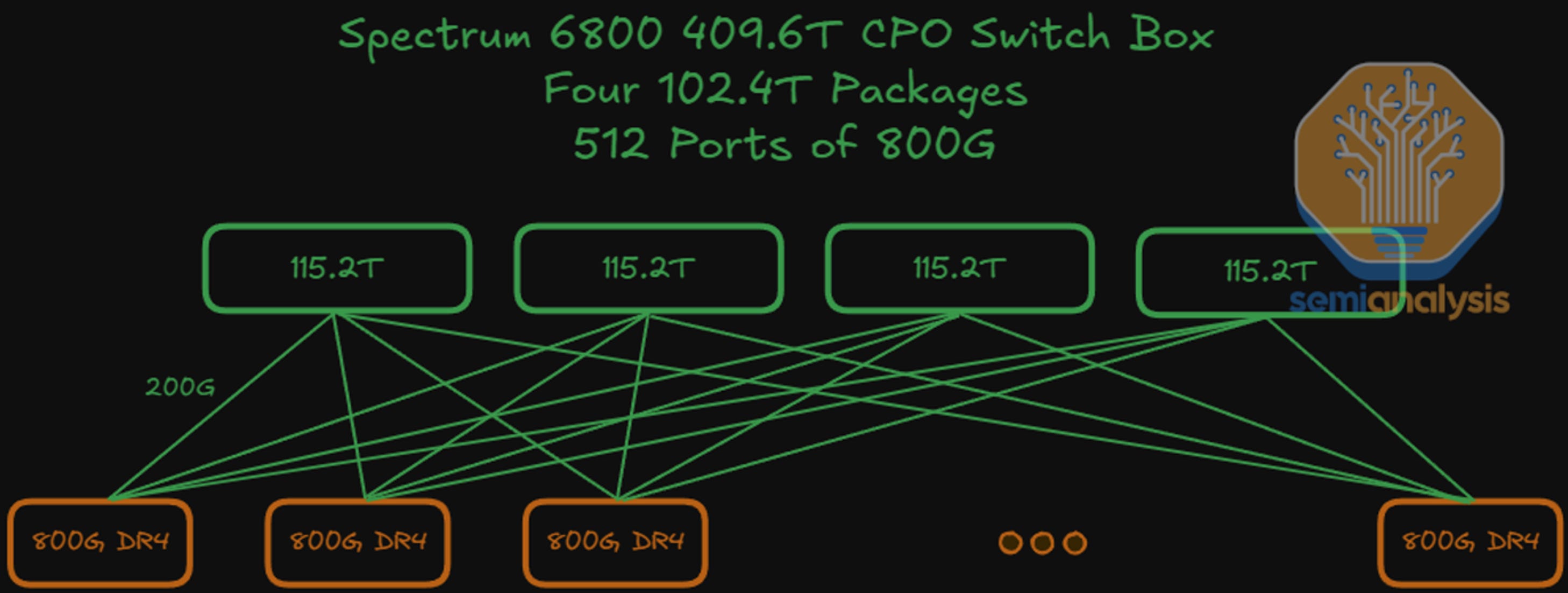
SN6800, a 4 ASIC, 2048-radix 409.6T multi-plane CPO switch, offering 512 ports of 800G;
SN6810, a high-radix 102.4T CPO switch with three further deployment options: 512 ports of 200G, 256 ports of 400G and 128 ports of 800G.
For the SN6600 switch, the scale-out reference architecture is an 8-plane network where each GPU fans out eight ways to eight different planes. This is similar to the reference architecture for the 8-plane scale-out network using SN6810 switches.
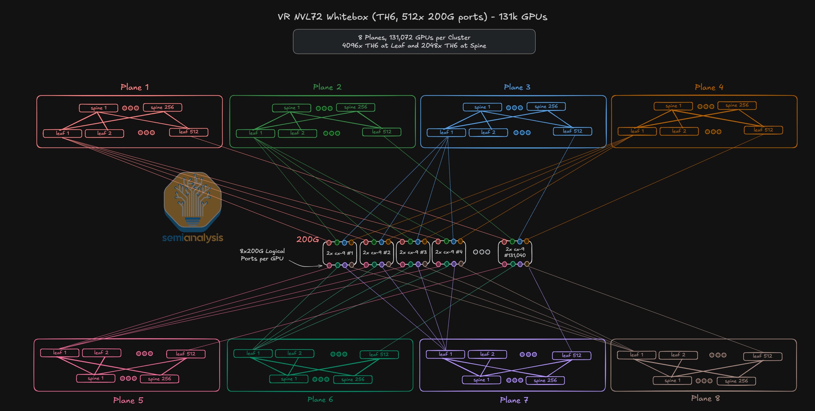
We think that the SN6800 switch with 512 ports of 800G will be quite attractive to Neoclouds because it simplifies deployments. Similar to the X800-Q3400 scale-out network, an SN6800 scale-out network could consist of two switch planes though the SN6800 enables a much larger feasible scale-out world size.
The diagram below shows what such a network could look like – though it only shows one of two planes as readers can deduce by the fact that we are only depicting 1x800G from each GPU. Note also that each SN6800 switch box consists of four ASICs, each with its own switch plane, which we will elaborate on later in the article.
For a 512-port switch, we can connect up to 131,072 GPUs with two layers of switches or a ludicrous 33,554,432 GPUs on 3 layers.
What advantages do CPO switches such as the SN6800 deliver for Neoclouds like Coreweave and Lambda when it comes to large-scale cluster deployments?
As discussed in our recent deep dive article on co-packaged optics, the first reason is that a significant amount of power can be saved by eliminating most of the transceiver content. If we compare the power consumption of one 800G DR4 optical transceiver (16-17W) to the power required by optical engines (OEs) and external light source (ELS) modules to delivery an equivalent 800G of bandwidth in the scale-out network, we see an average ~70% reduction in power used for optical transceivers. Taking a step back, this would translate to 10% in savings for the total networking equipment power consumption in a 3-Layer HGX Rubin NVL8 cluster. This reduction in networking equipment power consumption is however relatively insignificant and amounts to only ~1% of total cluster power consumption because the server’s power budget dominates the equation.
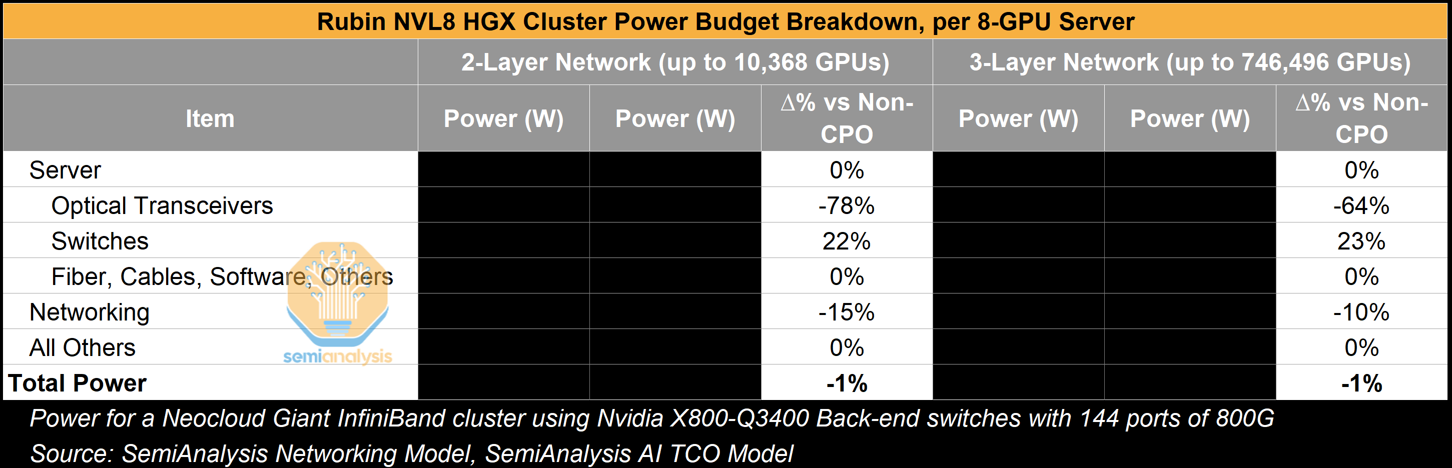
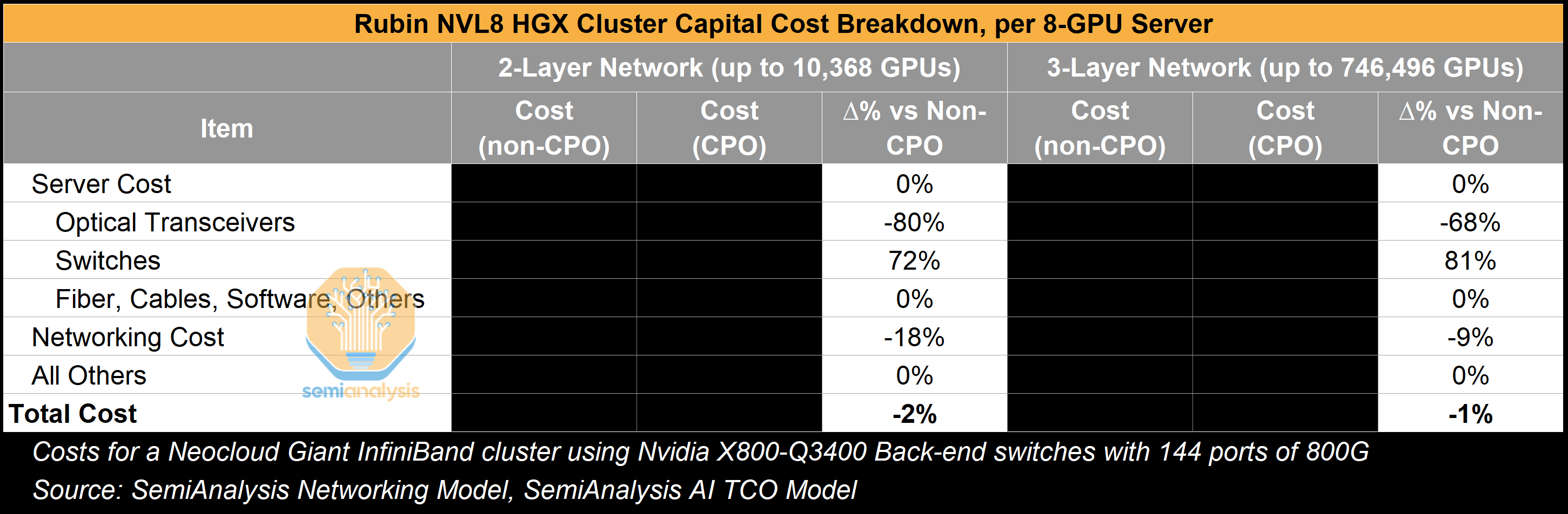
The second benefit is a reduction in cost stemming from eliminating almost all transceivers. There is even more room for price reduction if we are looking at NVIDIA LinkX transceivers, which tend to be priced at significant premium to their generic equivalent. If we compare total networking costs for a 3-Layer network with and without CPO-based switches in the scale-out domain, we see an average of ~75% reduction in transceiver costs. However, as with the power savings above, such costs savings tend not to move the needle dramatically considering the full cluster costs.
We outline these calculations in more detail and discuss this topic at greater length in our CPO Book Report.
Increased overall network reliability is another compelling point. Transceivers can be unreliable, with a large cluster certain to have ongoing link flaps. Meta’s study presented at ECOC showed strong reliability results over 15M 400G port-device hours, which is about equivalent 15 CPO switches tested for 11 months in a lab. It is an encouraging start – but we think this point could get stronger with more in field test deployments.
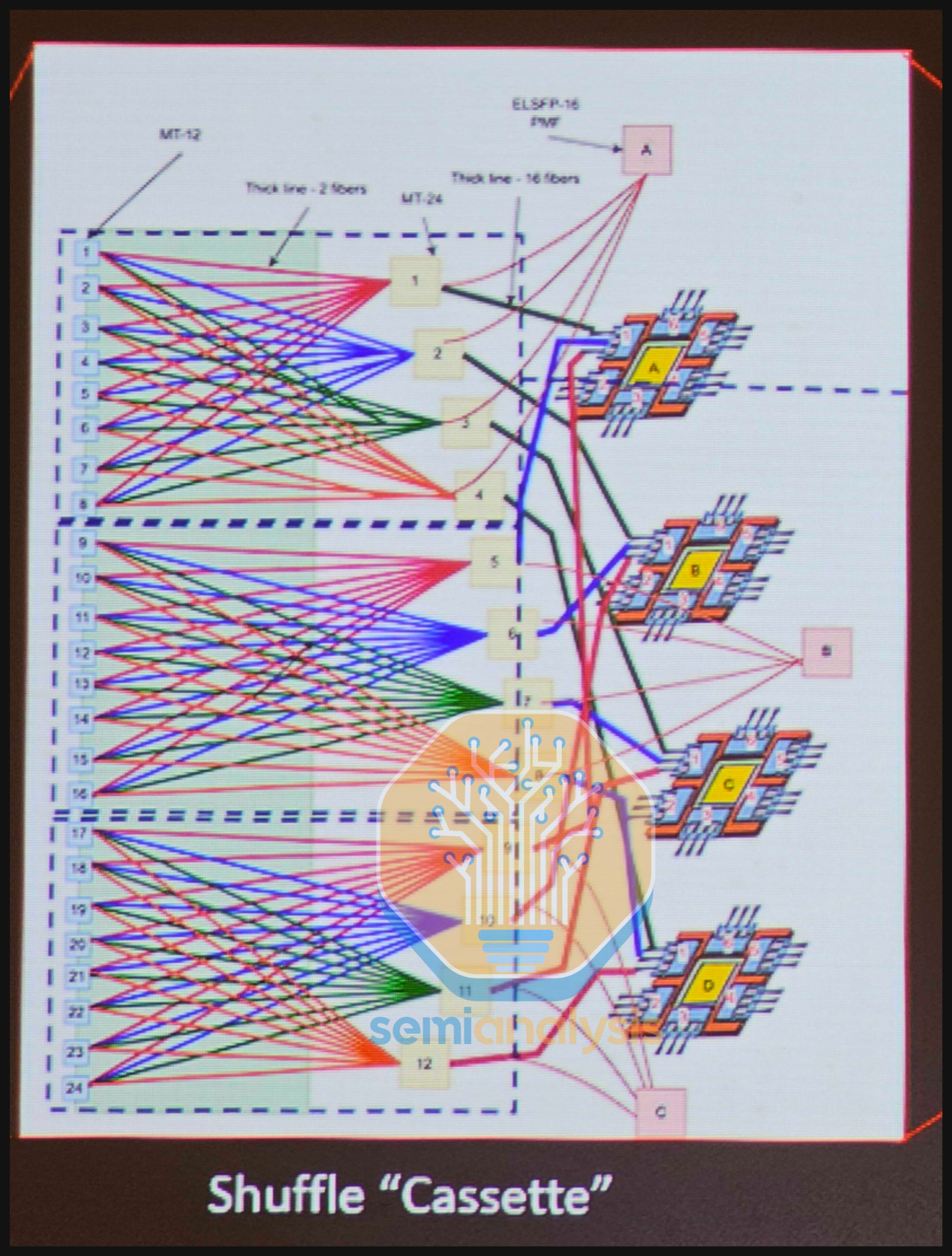
The last factor in favor of adoption of CPO that we would like to mention is the fact that some of Nvidia’s CPO switch SKUs contain the integrated fiber shuffle and can simplify the installation and maintenance of multi-plane network architectures. Recall that the SN6800 contains four Switch ASICs in a multi-plane configuration connected to ports via an integrated fiber shuffle, delivering 409.6T aggregate bandwidth, while the SN6810 uses one Switch ASIC, but without any integrated fiber shuffle, to deliver 102.4T aggregate bandwidth.
But first, we will explain why we think multi-plane networking architectures are here to stay as an important preface.
Large-scale cluster deployments where cluster sizes exceed 100k GPUs typically utilize multi-plane network architectures because single-plane network architectures do not have enough logical ports at current switch generations to support larger networks without resorting to a high number of switch layers of 3 or more layers.
Recall from above that a Vera Rubin NVL72 cluster built with Q3400-X800 switches at 1.6T logical ports per GPU cannot scale beyond the maximum cluster size of 93,312 GPUs. Even if future switch generations continue to double the maximum possible switching capacity per switch box, the per GPU bandwidth is also expected to double, which means that the effective logical port count in a cluster network is unlikely to change.
What this means is that deployment of large-scale GPU clusters will continue to require multi-plane network architectures. Do note however that multi-plane networking architectures are not limited by size and we have also seen NVIDIA reference architecture deployments with multi-plane clusters that are significantly below 100k GPUs each.
In multi-plane network architectures using the SN6600 switch instead of the CPO switch, each GPU fans out to multiple switch boxes using fiber shuffles. This requires customers to deploy shuffle boxes, patch panels and unwieldy octopus cables outside the switch box that introduce complexity in installation and maintenance.
Some of Nvidia’s CPO SKUs – such as the SN6800 and Q3450 –contain such a fiber shuffle within the switch box, with each optical engine fanning out to different logical ports. They therefore deliver higher aggregate bandwidth – 409.6T and 115.2T respectively than is possible with a switch box based on a single Switch ASIC.
For the SN6800 CPO switch, even though the bandwidth engine responsible for converting electrical to optical signals scales from 1.6T to 3.2T or 2x compared to the SN6600 switch, each 3.2T OE within the SN6800 switch box is split into four 800G logical ports that fan out within the box itself and exit the front panel through fiber connectors. This allows a single 1.6T GPU to fan out to two independent switch planes. In fact, the SN6800 switch box consists of four ASICs, which is similar to the X800-Q3400 switch box.
As the per GPU bandwidth continues to scale to 3.2T, it is not hard to imagine a 4-plane network using SN6800 switches, where each 3.2T GPU is split four ways to connect to four different switch boxes at 800G per link.
In fact, if you have not already noticed – there are strong parallels between the X800-Q3400 switch (non-CPO) explained earlier in the article and a CPO switch in that both facilitate high-radix, multi-plane networking architectures while encasing within the box complex cabling that saves customers on the hassle of cable management.
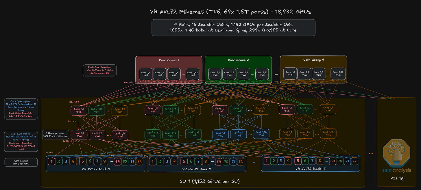
Outside of the NVIDIA ecosystem, the main switch ASIC players are Broadcom, which will be manufacturing the Tomahawk 6 and Tomahawk 6 CPO ASICs, as well as Cisco, which recently announced the G300 102.4T ASIC. There are two flavors of hyperscaler backend network deployments:
8-plane “flat” network utilizing the full 512 switch radix;
Single plane network with 1.6T OSFP cages at the NIC.
Source: SemiAnalysis AI Networking Model

For Meta, we think the VR NVL72 deployments will comprise only of non-scheduled fabric (NSF) clusters built using Tomahawk 6-based Minipack-4 OCP Rack 102.4T switches in each datacenter. While Meta will be using optics to connect all the switches within its cluster, it will use 1.6T AECs for NIC-to-TOR connections once 1.6T AECs become broadly available in the market. We expect the 1.6T AEC ramp to happen in the second half of calendar year 2026.
The catch is that 102.4T Minipack-4 switches may not be shipped in time for Vera Rubin NVL72 rack deployments, and if this were to be the case, some NSF clusters will be shipped using 51.2T Minipack-3 switches instead. This means that gearboxes within the AECs will have to be used to convert 200G per lane SerDes speed at the NIC to 100G per lane SerDes speed at the switch.
Meta will not be the only hyperscaler using 1.6T AECs for its VR200 deployments, however. We think xAI will use 1.6T AECs for both NIC-to-TOR and switch-to-switch connectivity at the leaf, spine and core layers. It will be a single-plane network replacing most 1.6T transceivers at the switch boxes – and this can give Credo plenty of pricing power.
Hyperscaler Customization and Assembly Logistics
Customization
For GB300, although the reference design has four ConnectX-8 NICs for the backend network and one Bluefield-3 for frontend network, most hyperscalers have their own design and alternative networking configurations, especially for Bluefield-3. Beside networking configuration, the power delivery modules, the local NVMe storage, and the management module are also highly customized and differentiated across customers.
For example, for some racks, even Amazon is deploying ConnectX-8 in GB300s in many cases. Also, most hyperscalers are deploying their in-house DPU instead of Bluefield-3 for frontend networking. The power delivery module and management modules in GB300 are also highly customized as every customer has differing preferences for these modules. As such, the front half of GB300 is highly customizable with each hyperscalers’ design differing from each other significantly.
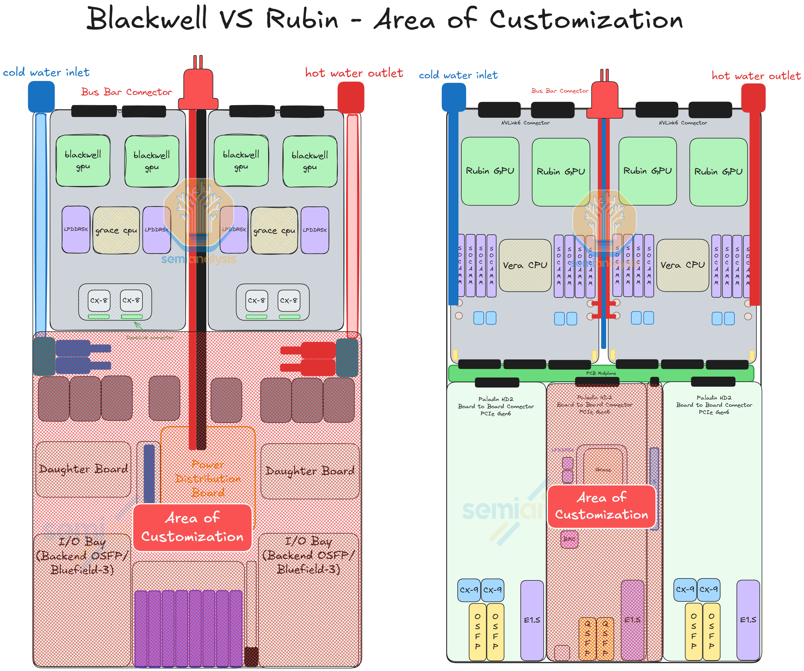
For VR NVL72, although some level of customization is still available, there are a lot more limitations on the form factor. Given the modular and the cableless design of VR NVl72, the customized modules at the front of the chassis must match the form factor and dimension of Nvidia’s reference design. The modules available for customization are power delivery, Bluefield-4, and management modules. We expect most hyperscaler customers to adopt their in-house DSP instead of Bluefield-4. Given the limitation on form factor and dimensions, hyperscalers are redesigning the board layout and module form factor of their in-house DPU to match that of Bluefield-4. For the power delivery modules and management, some customers are also looking to combine them. Amazon does have a JBOK / Nitro Box NIC version for VR NVL72
Assembly Automation and Logistics
At CES 2026, Jensen mentioned that with the streamlined cableless design and automation assembly process, compute tray assembly time has significantly reduced from 2 hours to 5 minutes from Blackwell to Rubin. There are only three L10 level compute tray assembly partners with automation capability for the Rubin platform – Foxconn, Quanta, and Wistron.
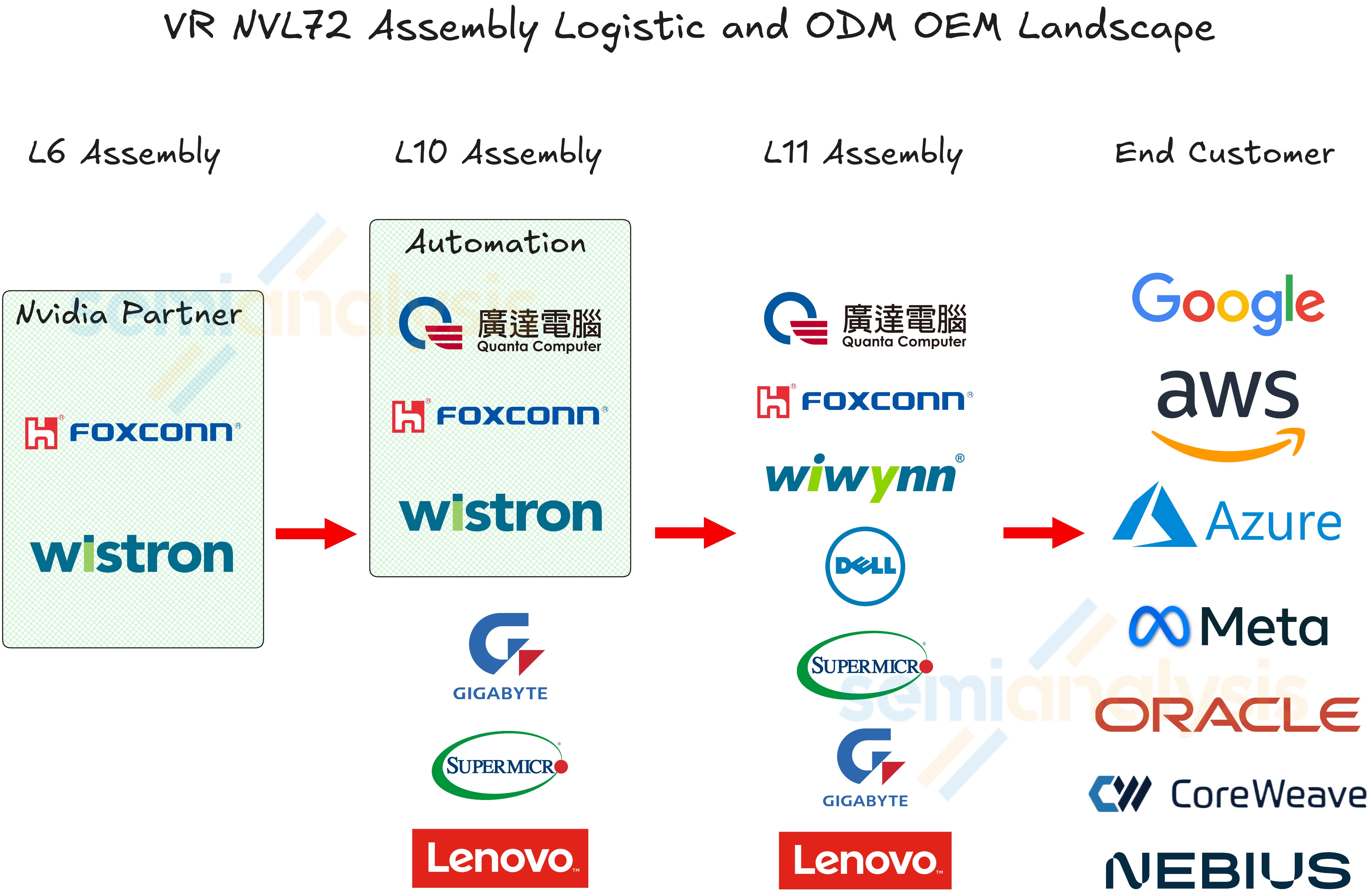
At L6, board level PCBA, Wistron and Foxconn are the main supplier of Blackwell and Rubin. For L10, Blackwell had lots of different compute tray manufacturers as they buy the Bianca boards from Nvidia to sell to their clients. For Rubin, there are only three suppliers that have the capability to do automation of Rubin compute tray. For smaller ODM or OEM, they either have their compute tray made at the three automation suppliers mentioned above or they will do it in-house without automation. Although not as efficient, compute tray assembly without automation should be much easier compared to Blackwell as well given the seamless modular design. Then at L11, the various ODMs/OEMs assemble the compute tray into the rack.
VR NVL72 TCO: BoM and Power Budget Analysis
The VR NVL72 Component BoM and Power Budget Model provides a detailed analysis on the BoM and the Power Budget of the rack system.
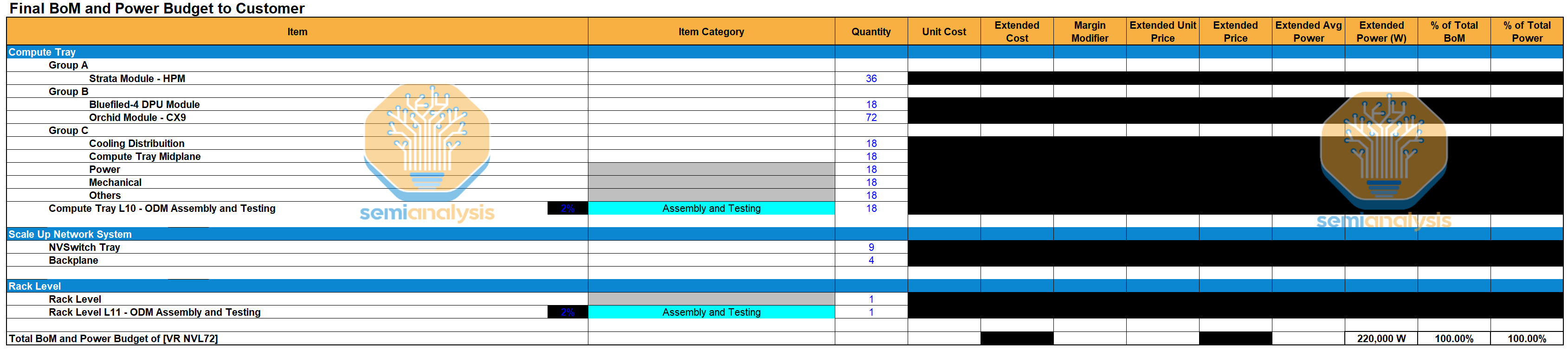
The VR NVL72 is more expensive on a per-GPU capital cost basis, ~45% higher vs GB300s and ~14-15% higher vs the MI4XX given a higher server cost on a per GPU basis. This results in a higher Capital Cost of Ownership (TCO). For example VR NVL 72 Hyperscaler Arista has a capital cost of $3.28 to MI4XX Hyperscaler of $2.86 per hour per GPU over a 4 year useful life. Our TCO Model runs on a 4y useful life for the purpose of calculating capital cost per hour to reflect a conservative business case, but most Neoclouds and Hyperscalers will use a 5-6y depreciation period and we think it is best to look at EBIT margins using this depreciation period. Our preferred yardstick is Project IRR, which is agnostic to the chosen depreciation period.
However, one advantage for Nvidia’s VR SOCAMM option is that NVIDIA directly procures memory, allowing them to negotiate long-term agreements, volume-preferential terms with memory suppliers and most importantly, VVIP pricing. We think this will shield end customers from spikes in memory costs as we outline in our AI server apocalypse note, and is another example of how, as the Central Bank of AI, Nvidia is effectively hedging DRAM prices for all of its customers.
By contrast, AMD is much more exposed to DRAM price increases as it has about double the amount of DRAM, with about 55 TB per rack of LPDDR5 and 55 TB per rack of DDR5. For the AMD’s Helios rack scale system, AMD sells the GPU/board and does procure the LPDDR5 memory, but it does not procure DDR5 DRAM for rack compute trays; rack assemblers/ODMs source and integrate DDR5 memory. This leaves buyers of AMD’s racks more exposed because AMD is only able to potentially “hedge” the LPDDR5 portion via long-term contracts leaving the DDR5 portion completely exposed. Having double the DRAM content also nearly doubles the overall exposure.
Helios memory costs are more likely to be passed through or re-priced by assemblers and therefore exhibit greater hikes in a memory upcycle. Therefore, we model lower memory price hikes for VR and GB compared to MI4XX below. Our MI400 rack assumptions reflect $8.70/GB LPDDR pricing for AMD versus $6.77/GB for Nvidia, embedding volume discount structures vs the market contract price of $10.63/GB but reflecting the slack of volume economics vs NVIDIA.
Our AI Memory Model expects significant increases in LPDDR5 and DDR5 contract prices into 2Q26 and beyond and we expect to make further revisions higher in total server capex.
NVIDIA’s 2300W configuration represents the Max-P configuration, while the efficiency optimized Max-Q configuration runs at 1800W. Regardless of which configuration Nvidia claims both can hit the same peak clocks and therefore achieve marketed 50 PFLOPS FP4 performance. While the underlying hardware is the same, the TCO implications are due to operating costs from different levels of power consumption.
Below we share detailed numbers on cost of servers, storage, networking, etc as well as what Nvidia plans to do with Groq.